Organization of bus infrastructure connecting the agents of the system interface STI version 1.0
The article outlines the principles for building the infrastructure of a local system bus connecting agents of a single junction segment of a simple performer of STI version 1.0 in a VLSI crystal or FPGA volume. The organization of the address decoder, the data bus switches and the artist selection is considered. An example of the description of the bus infrastructure of the STI segment in the Verilog language is given. Offered options for connecting performers to bus segments with a lower data width.
The interface of a simple performer - Simple Target Interface (hereinafter - STI) is a set of logical signals and an interaction protocol that provides the connection of several functional blocks in the scope of a single FPGA configuration project or VLSI chip (hereinafter referred to as the project). The specification of the STI interface version 1.0 was published in article [1].
The terminology used below was introduced into the specification and the basic principles of connecting STI performers to the initiator within one segment were defined.
As an example, it is proposed to consider the segment 64-p of the STI bus, which unites the initiator and four performers. In this case, two performers have data width of 32 and 8 bits. The structural diagram of this STI segment is presented in Fig. one.

Fig. 1. Structural diagram of the STI segment
')
The composition of each artist includes the resources available for receiving data when writing and generating data when reading. These resources can be represented by registers, memory blocks, interface bridges. Each such resource has its own address in the corresponding address space. Memory blocks, register files and interface bridges can occupy a range of consecutive addresses from the address space.
Consider an example in which four contractors have resources in the I / O address space and memory. The distribution of address ranges by performers is shown in Table 1.
Table 1.
The functional diagram of the organization of the bus infrastructure of the STI segment is shown in Fig. 2
The selection of the artist according to the current address and the command code (the command determines the address space) is performed by the address decoder - address decoder. The unit at the first output of the address decoder signals the call to the executor-A, the unit at the second exit - to the executor-B, etc. The binary code at the output of the decoder is shown in Table 1.
The outputs of the address decoder control the sampling signals of the performers: FB1_EN, FB2_EN, FB3_EN and FB4_EN for Target-A, Target-B, Target-C and Target-D, respectively. Each of these signals is sent to the logic gate-I, which allows the passage of the request signal S_EX_REQ to the selected performer, and also to the switching node - multiplexer (MUX).
The multiplexer commutes the outputs of the performers (S_EX_ACK and S_D_RD) to the inputs of the initiator. In this case, at each time point, the initiator must receive signals only from one performer (selected by the decoder), or all units must be supplied. The latter requirement is due to the fact that the initiator’s address to an address that does not belong to any performer should not cause the system to “hang” due to the presence of zero at the S_EX_ACK input. Reading data from a non-existent resource in most systems returns a combination of all units.
The decoder and the multiplexer are combinational logic circuits that operate within one clock cycle (between adjacent rising edges).
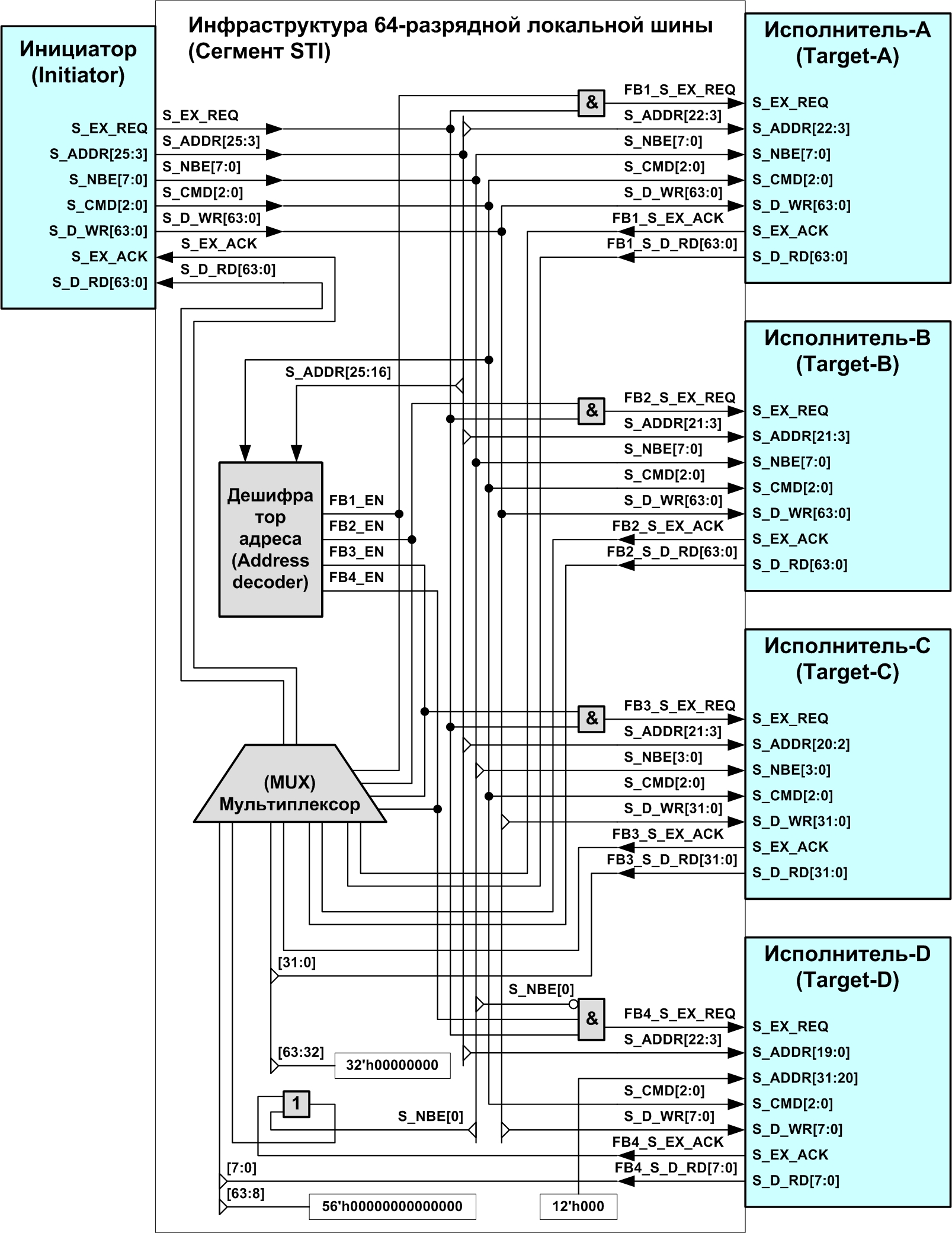
Fig. 2. Functional diagram of the organization of the bus infrastructure of the STI segment
It should be noted separately that the performer-D does not have an input sampling of S_NBE, since it is equipped with an 8-bit STI interface. As a result, the sampler-D is sampled taking into account the activity of the data bus byte to which this artist is connected. From the functional diagram it can be seen that the low byte of the data bus is used, therefore the performer-D is available only if the low byte of data is active: S_NBE [0] = "0". The logical OR gate at the executor's output S_EX_ACK passes the ready signal to the multiplexer also under the condition S_NBE [0] = "0". Otherwise, the multiplexer receives a high level, preventing "freezing".
A 32-bit artist-C connection to a 64-bit STI segment is implemented using the lower half of data buses [31: 0]. For bytes with the offset of the address 0, 1, 2, and 3 transmitted over these data lines, the byte enable signals S_NBE [3: 0] correspond. In this case, the byte enable signals do not participate in the generation of the activation signal of the contractor FB3_S_EX_REQ, because the cycles of accessing the upper half of the data bus (bytes with address offset 4, 5, 6 and 7) will cause an empty loop on the 32-bit interface of the performer-C, with which all four low bytes are deactivated. STI contractor is obliged to correctly respond to such a cycle.
but,
b,
at
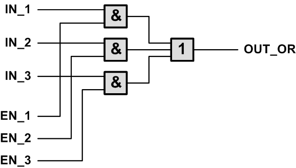
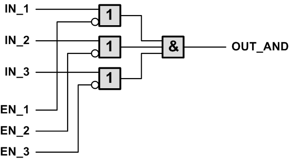
Fig. 3. The logical organization of the multiplexer
Consider the organization of a multiplexer that commutes the performers output signals to the inputs of the initiator. The canonical multiplexer scheme is based on the principle of DNF (disjunctive normal form of the function in binary algebra). The scheme on the basis of DNF consists of two cascades. The first cascade includes valves AND (conjunction in the formula of DNF), and the second cascade - the unifying element OR (disjunctions in DNF). Such a scheme for a three-input multiplexer is shown in Fig. 3, a. The principle of operation of a multiplexer based on DNF consists in passing the units by the first stage only from the selected input. When none of the multiplexer inputs is selected, this scheme will produce a low level at the output, which does not meet the above requirements for the S_EX_ACK signal switch.
The second variant of multiplexer organization is shown in fig. 3, b. This scheme is based on the principle of CNF (conjunctive normal form) and consists of two stages, the first of which includes OR valves, which pass a logical zero only from the selected input, and the second stage contains the combining element AND operating according to the principle: at least one zero is output zero. It is easy to see that with all the zeros at the inputs of the resolution, when no performer is selected, such a multiplexer outputs one at the output, satisfying the requirements of the S_EX_ACK signal at the initiator input.
It is a multiplexer based on CNF that is recommended to be used when describing the bus infrastructure of a simple contractor interface - STI.
In some bases of VLSI elements and early FPGA architectures, it is allowed to use elements with three states at the output (tristable buffers) not only in I / O blocks, but also in the core. The tristable buffer in the example in fig. 3, transmits the IN_x signal to the output in the presence of a unit at the control input EN_x, otherwise the output is in the third state - “Z”. A switch based on the S_EX_ACK shared link, which is controlled by tristable buffers, is shown in Fig. 3, c. Pull-up resistor sets the value of the signal on the shared communication line, in the case when all buffers are turned off (no performer selected). A pull-up resistor forms a logical unit in positive logic. Thus, the requirement for the S_EX_ACK signal switch is fulfilled.
It should be noted that from the point of view of the binary logic of the circuit in fig. 3, b and fig. 3, are identical on that set of input combinations, when the unit on the enabling inputs EN_x is present in no more than one position. In the switch of performers STI, only one performer can be selected, or none is selected, which corresponds to the requirement for the circuit in fig. 3, c. The scheme is similar to fig. 3b is formed by many HDL synthesizers automatically from the RTL model, similar to Fig.3, c.
Unused high-order bits of data on the C and D artist read buses, complementing the bit depth up to 64 bits, are set to zeros by a permanent connection to the “digital ground” circuit - GND.
Another interesting point in the functional diagram in Figure 2 is connected with the bus address of the contractor-D. In some cases, it is required to connect a previously developed library block with some versatility to the local system bus. For example, a memory block of a certain capacity that requires a corresponding address range, or an interface bridge designed for the full address format is 32 bits. If this block in the current system configuration uses an incomplete range of addresses, constants should be applied to the higher unused bits of the S_ADDR input. In our example, the unused inputs S_ADDR [31:20] of the executor -D are given zeros.
When an artist with a lower data width is connected to a segment with a higher bit width, the effect of alternating resource addresses of this artist with unused addresses appears. This is due to the feature of byte addressing. Bytes whose address ends with “000” will always be transmitted by bits [7: 0] of the 64-bit data bus, bytes with addresses ending with “001” bits [15: 8] are used, etc. ... for bytes with the address containing in the lower digits "111" data lines are used [63:56]. Thus, the addresses corresponding to the unused data bus lines will alternate with the addresses of the artist resources available on the remaining lines.
Based on the above, the resources of the executor-C will be located at the addresses, the hexadecimal representation of which ends with the numbers 0 ... 3 and 8..B, and between the "neighboring" resources of the executor-C there will be 4 unused bytes, access to which is performed via data lines [63 : 32].
Similarly, performer-D resources will be available at addresses ending in 0h and 8h, in increments of +8.
It should be noted that the connection of performers C and D is implemented with an offset of the address bus by 1 and 3 bits, respectively. In other words, the address of the 32-bit data word for the performer-C becomes the address of the 64-bit data word in the STI segment, and the byte address in the volume of the performer-D also becomes the address of the 64-bit word in the STI segment.
In order to connect a performer with a lower data bus width to the STI segment, so that its resources are located in the address space of the system (processor) sequentially and continuously, you need to use an additional functional block - a bridge that breaks the circulation cycle with a higher data width by 2 or more Cycle with bit data executor of the exchange. The organization of such a bridge is beyond the scope of this article.
Below is an example of a description of the infrastructure of the STI segment, shown in Fig. 2, in the Verilog language:
Actually the infrastructure of the STI segment is described in the code block, limited to the comment “STI Bus Infrastructure”.
The STI interface allows you to connect artists with a larger data bus width to a segment with a lower bit depth. Consider an example of connecting a 64-bit artist to a segment with 16-bit data buses. The functional diagram of such a connection is shown in Fig. four.

Fig. 4. Connecting a 64-bit artist to a 16-bit STI segment
When connecting the contractor with a higher data width, there is no need to shift the address bus bits. Instead, the low-order address bits that are not used by the executor control the switching nodes that select the part of the data bus that is being exchanged for the current address. In this case, the resources of the contractor are located in the address space in the same order as when connecting to a segment of equal data width.
The switching nodes are represented by a demultiplexer (DMX), buffers duplicating the data write bus of the S_D_WR segment into the corresponding equal groups of artist write bus bits, and a multiplexer (MX) of the data read bus.
The demultiplexer passes the resolution signals of the S_NBE bytes of the STI segment to the corresponding inputs of the resolution of the artist's bytes based on the lower-order bits of the address. In this example, the low-order bits of the switching control address are S_ADDR [2: 1]. At the outputs of the demultiplexer, which are not selected by the current S_ADDR combination [2: 1], logical units are formed that prohibit accessing bytes whose address on a 16-bit bus does not correspond to the current address.
The functional diagram of the demultiplexer, corresponding to the configuration in fig. 4 is shown in fig. five.

Fig. 5. The functional diagram of the demultiplexer
The multiplexer is a standard logical combinational node that commutes one of the input signals to the output, depending on the control combination - the lower bits of the address. So, when S_ADDR [2: 1] = 0h, the performer S_D_RD [15: 0] signals are transmitted to the S_D_RD [15: 0] output; when S_ADDR [2: 1] = 1h, the S_D_RD [31:16] signals are transmitted; when S_ADDR [2 : 1] = 2h - signals S_D_RD [47:32], with S_ADDR [2: 1] = 3h - signals S_D_RD [63:48].
Connection of 16.32 and 64 bit artists to the 8-bit STI segment is slightly different, because there is no S_NBE byte sampling signal in such a segment. If a specific byte is not accessed, the corresponding exchange cycle is not formed on the 8-bit segment.
An example of connecting a 16-bit artist to an 8-bit segment is illustrated in Fig. 6
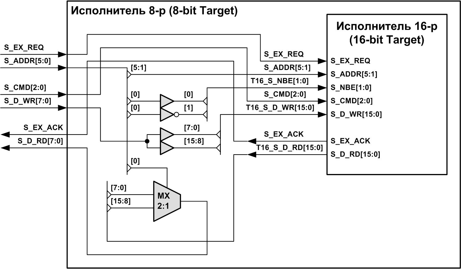
Fig. 6. Connecting a 16-bit artist to an 8-bit STI segment
The byte enable signals S_NBE for a 16-bit artist create a 1: 2 address decoder built on a buffer and an inverter. When referring to the lower (even) byte, the address bit S_ADDR [0] contains zero passing through the buffer to the input of the contractor S_NBE [0]. Thus, the exchange of data over lines [7: 0] is permitted. At the same time, at unit S_NBE [1], a unit is formed that prohibits the exchange over data lines [15: 8]. When accessing the most significant (odd) byte of the contractor, the address bit S_ADDR [0] contains one, which leads to the opposite situation, when the exchange is carried out along the lines [15: 8].
The multiplexer - MX commutes to the 8-bit data read bus S_D_RD one of the two bytes of the artist read output as follows: when the address bit S_ADDR [0] is zero, the data [7: 0] is sent from the artist output, and if one, the data [15: 8].
Data for recording is duplicated on both bytes of the contractor S_D_WR, but only one byte is recorded, depending on S_ADDR [0] and S_NBE [1: 0], respectively.
When connected to an 8-bit STI segment of a 32-bit artist, the address decoder has a 2: 4 format (with inverse outputs) and converts the address bits S_ADDR [1: 0] to S_NBE [3: 0]. In this case, the multiplexer has a 4: 1 format and is also controlled by the bits of the S_ADDR [1: 0] address. When a 64-bit artist is connected, a 3: 8 decoder (with inverse outputs) converts the bits of the S_ADDR [2: 0] address into the byte resolution signals S_NBE [7: 0]. The 8: 1 multiplexer commutes bytes on the data reading bus according to a combination of the three least significant bits of the address.
Findings.
The interface of the interface of the simple executor STI uses the bus infrastructure, simple and convenient in the description in Verilog and VHDL, combining the initiator and performers of the STI within one segment.
The description of the address decoder at the behavioral level of abstraction using conditional if / case operators allows you to avoid time-consuming synthesis of combinational circuits using Boolean algebra methods.
The protocol of interaction of agents STI allows the use of artists with different width of the address and data tires in one bus segment.
Bibliography
1. Borisenko N.V. Synchronous system interface of the interaction of computational cores with peripheral blocks of a VLSI crystal. "Components and Technologies" №10.2016.
2. RTL Hardware Design Using VHDL: Coding for Efficiency, Portability, and Scalability. By Pong P.Chu. John Wiley & Sons, Inc. 2006
3. Borisenko N.V. Approaches to the organization of a unified series of synthesized models of FIFO buffers implemented in various families of programmable logic. Part 1. "Components and technologies" №12.2012.
4. Borisenko N.V. Schemes for including FIFO buffers with a unified interface in the data path between the source and receiver of information. "Components and Technologies" №2.2013.
5. Borisenko N.V. Organization of synchronous FIFO buffers with a unified interface, built on general-purpose registers in the volume of programmable logic chips. "Components and technologies" №8.2016.
The interface of a simple performer - Simple Target Interface (hereinafter - STI) is a set of logical signals and an interaction protocol that provides the connection of several functional blocks in the scope of a single FPGA configuration project or VLSI chip (hereinafter referred to as the project). The specification of the STI interface version 1.0 was published in article [1].
The terminology used below was introduced into the specification and the basic principles of connecting STI performers to the initiator within one segment were defined.
As an example, it is proposed to consider the segment 64-p of the STI bus, which unites the initiator and four performers. In this case, two performers have data width of 32 and 8 bits. The structural diagram of this STI segment is presented in Fig. one.
Fig. 1. Structural diagram of the STI segment
')
The composition of each artist includes the resources available for receiving data when writing and generating data when reading. These resources can be represented by registers, memory blocks, interface bridges. Each such resource has its own address in the corresponding address space. Memory blocks, register files and interface bridges can occupy a range of consecutive addresses from the address space.
Consider an example in which four contractors have resources in the I / O address space and memory. The distribution of address ranges by performers is shown in Table 1.
Table 1.
| Executor | Address space | ADDR [25] | ADDR [24] | ADDR [23] | ADDR [22] | ADDR [21] | ADDR [20] | ADDR [19] | ADDR [18] | ADDR [17] | ADDR [16] | Capacity, bytes | DC_1 | DC_2 | DC_3 | DC_4 |
|---|---|---|---|---|---|---|---|---|---|---|---|---|---|---|---|---|
| Target_A | Memory | one | 0 | 0 | X | X | X | X | X | X | X | 8M | one | 0 | 0 | 0 |
| Target_B | Memory | 0 | 0 | 0 | 0 | X | X | X | X | X | X | 4M | 0 | one | 0 | 0 |
| Target_C | Memory | one | 0 | one | one | X | X | X | X | X | X | 4M | 0 | 0 | one | 0 |
| Target_D | Memory | one | 0 | one | 0 | 0 | 0 | one | 0 | one | one | 64K | 0 | 0 | 0 | one |
| Target_D | I / O | one | 0 | 0 | X | X | X | X | X | X | X | 8M | 0 | 0 | 0 | one |
| Target_C | I / O | 0 | 0 | 0 | 0 | X | X | X | X | X | X | 4M | 0 | 0 | one | 0 |
| Target_B | I / O | one | 0 | one | one | X | X | X | X | X | X | 4M | 0 | one | 0 | 0 |
| Target_A | I / O | one | 0 | one | 0 | 0 | 0 | one | 0 | one | one | 64K | one | 0 | 0 | 0 |
The functional diagram of the organization of the bus infrastructure of the STI segment is shown in Fig. 2
The selection of the artist according to the current address and the command code (the command determines the address space) is performed by the address decoder - address decoder. The unit at the first output of the address decoder signals the call to the executor-A, the unit at the second exit - to the executor-B, etc. The binary code at the output of the decoder is shown in Table 1.
The outputs of the address decoder control the sampling signals of the performers: FB1_EN, FB2_EN, FB3_EN and FB4_EN for Target-A, Target-B, Target-C and Target-D, respectively. Each of these signals is sent to the logic gate-I, which allows the passage of the request signal S_EX_REQ to the selected performer, and also to the switching node - multiplexer (MUX).
The multiplexer commutes the outputs of the performers (S_EX_ACK and S_D_RD) to the inputs of the initiator. In this case, at each time point, the initiator must receive signals only from one performer (selected by the decoder), or all units must be supplied. The latter requirement is due to the fact that the initiator’s address to an address that does not belong to any performer should not cause the system to “hang” due to the presence of zero at the S_EX_ACK input. Reading data from a non-existent resource in most systems returns a combination of all units.
The decoder and the multiplexer are combinational logic circuits that operate within one clock cycle (between adjacent rising edges).
Fig. 2. Functional diagram of the organization of the bus infrastructure of the STI segment
It should be noted separately that the performer-D does not have an input sampling of S_NBE, since it is equipped with an 8-bit STI interface. As a result, the sampler-D is sampled taking into account the activity of the data bus byte to which this artist is connected. From the functional diagram it can be seen that the low byte of the data bus is used, therefore the performer-D is available only if the low byte of data is active: S_NBE [0] = "0". The logical OR gate at the executor's output S_EX_ACK passes the ready signal to the multiplexer also under the condition S_NBE [0] = "0". Otherwise, the multiplexer receives a high level, preventing "freezing".
A 32-bit artist-C connection to a 64-bit STI segment is implemented using the lower half of data buses [31: 0]. For bytes with the offset of the address 0, 1, 2, and 3 transmitted over these data lines, the byte enable signals S_NBE [3: 0] correspond. In this case, the byte enable signals do not participate in the generation of the activation signal of the contractor FB3_S_EX_REQ, because the cycles of accessing the upper half of the data bus (bytes with address offset 4, 5, 6 and 7) will cause an empty loop on the 32-bit interface of the performer-C, with which all four low bytes are deactivated. STI contractor is obliged to correctly respond to such a cycle.
but,
b,
at
Fig. 3. The logical organization of the multiplexer
Consider the organization of a multiplexer that commutes the performers output signals to the inputs of the initiator. The canonical multiplexer scheme is based on the principle of DNF (disjunctive normal form of the function in binary algebra). The scheme on the basis of DNF consists of two cascades. The first cascade includes valves AND (conjunction in the formula of DNF), and the second cascade - the unifying element OR (disjunctions in DNF). Such a scheme for a three-input multiplexer is shown in Fig. 3, a. The principle of operation of a multiplexer based on DNF consists in passing the units by the first stage only from the selected input. When none of the multiplexer inputs is selected, this scheme will produce a low level at the output, which does not meet the above requirements for the S_EX_ACK signal switch.
The second variant of multiplexer organization is shown in fig. 3, b. This scheme is based on the principle of CNF (conjunctive normal form) and consists of two stages, the first of which includes OR valves, which pass a logical zero only from the selected input, and the second stage contains the combining element AND operating according to the principle: at least one zero is output zero. It is easy to see that with all the zeros at the inputs of the resolution, when no performer is selected, such a multiplexer outputs one at the output, satisfying the requirements of the S_EX_ACK signal at the initiator input.
It is a multiplexer based on CNF that is recommended to be used when describing the bus infrastructure of a simple contractor interface - STI.
In some bases of VLSI elements and early FPGA architectures, it is allowed to use elements with three states at the output (tristable buffers) not only in I / O blocks, but also in the core. The tristable buffer in the example in fig. 3, transmits the IN_x signal to the output in the presence of a unit at the control input EN_x, otherwise the output is in the third state - “Z”. A switch based on the S_EX_ACK shared link, which is controlled by tristable buffers, is shown in Fig. 3, c. Pull-up resistor sets the value of the signal on the shared communication line, in the case when all buffers are turned off (no performer selected). A pull-up resistor forms a logical unit in positive logic. Thus, the requirement for the S_EX_ACK signal switch is fulfilled.
It should be noted that from the point of view of the binary logic of the circuit in fig. 3, b and fig. 3, are identical on that set of input combinations, when the unit on the enabling inputs EN_x is present in no more than one position. In the switch of performers STI, only one performer can be selected, or none is selected, which corresponds to the requirement for the circuit in fig. 3, c. The scheme is similar to fig. 3b is formed by many HDL synthesizers automatically from the RTL model, similar to Fig.3, c.
Unused high-order bits of data on the C and D artist read buses, complementing the bit depth up to 64 bits, are set to zeros by a permanent connection to the “digital ground” circuit - GND.
Another interesting point in the functional diagram in Figure 2 is connected with the bus address of the contractor-D. In some cases, it is required to connect a previously developed library block with some versatility to the local system bus. For example, a memory block of a certain capacity that requires a corresponding address range, or an interface bridge designed for the full address format is 32 bits. If this block in the current system configuration uses an incomplete range of addresses, constants should be applied to the higher unused bits of the S_ADDR input. In our example, the unused inputs S_ADDR [31:20] of the executor -D are given zeros.
When an artist with a lower data width is connected to a segment with a higher bit width, the effect of alternating resource addresses of this artist with unused addresses appears. This is due to the feature of byte addressing. Bytes whose address ends with “000” will always be transmitted by bits [7: 0] of the 64-bit data bus, bytes with addresses ending with “001” bits [15: 8] are used, etc. ... for bytes with the address containing in the lower digits "111" data lines are used [63:56]. Thus, the addresses corresponding to the unused data bus lines will alternate with the addresses of the artist resources available on the remaining lines.
Based on the above, the resources of the executor-C will be located at the addresses, the hexadecimal representation of which ends with the numbers 0 ... 3 and 8..B, and between the "neighboring" resources of the executor-C there will be 4 unused bytes, access to which is performed via data lines [63 : 32].
Similarly, performer-D resources will be available at addresses ending in 0h and 8h, in increments of +8.
It should be noted that the connection of performers C and D is implemented with an offset of the address bus by 1 and 3 bits, respectively. In other words, the address of the 32-bit data word for the performer-C becomes the address of the 64-bit data word in the STI segment, and the byte address in the volume of the performer-D also becomes the address of the 64-bit word in the STI segment.
In order to connect a performer with a lower data bus width to the STI segment, so that its resources are located in the address space of the system (processor) sequentially and continuously, you need to use an additional functional block - a bridge that breaks the circulation cycle with a higher data width by 2 or more Cycle with bit data executor of the exchange. The organization of such a bridge is beyond the scope of this article.
Below is an example of a description of the infrastructure of the STI segment, shown in Fig. 2, in the Verilog language:
`timescale 1ns / 1ps //////////////////////////////////////////////////////////////////////// // Engineer: FPGA-Mechanic // // Create Date: 09:38:35 03/03/2017 // Design Name: Argon SoC Proto // Module Name: STI_EXAMPLE // Project Name: Argon Otd.23 Projects // Target Devices: Any FPGA or ASIC // Tool versions: Xilinx 14.7 // Description: Test-purpose synthesizable STI module // //////////////////////////////////////////////////////////////////////// module STI_EXAMPLE( input CLK, input RST ); // Internal signals declaration: // STI-64: wire S_EX_REQ, wire [25:3] S_ADDR, wire [7:0] S_NBE, wire [2:0] S_CMD, wire [63:0] S_D_WR, wire S_EX_ACK, wire [63:0] S_D_RD, //------------------------------------------ // Initiator: STI_64b_Initiator INITR( .CLK(CLK), .RST(RST), .S_EX_REQ(S_EX_REQ), .S_ADDR(S_ADDR), .S_NBE(S_NBE), .S_CMD(S_CMD), .S_D_WR(S_D_WR), .S_EX_ACK(S_EX_ACK), .S_D_RD(S_D_RD) ); //------------------------------------------ // STI Bus Infrastructure: reg FB1_EN, FB2_EN, FB3_EN, FB4_EN; wire FB1_S_EX_REQ, FB2_S_EX_REQ, FB3_S_EX_REQ, FB4_S_EX_REQ; wire [63:0] FB1_S_D_RD, FB2_S_D_RD, FB3_S_D_RD, FB4_S_D_RD; wire FB1_S_EX_ACK, FB2_S_EX_ACK, FB3_S_EX_ACK, FB4_S_EX_ACK; always @ (S_ADDR[25:16], S_CMD) if((~S_CMD[2] & S_CMD[0]) | (S_CMD[2] & ~S_CMD[1] & S_CMD[0]) | &(S_CMD[2:1])) // Memory CMD: 0X1,101,11X case(S_ADDR[25:23]) 3'b100 : // 100XXXXXXX begin FB1_EN <= 1'b1; FB2_EN <= 1'b0; FB3_EN <= 1'b0; FB4_EN <= 1'b0; end 3'b000 : // 000XXXXXXX if(S_ADDR[22] == 1'b0) // 0000XXXXXX begin FB1_EN <= 1'b0; FB2_EN <= 1'b1; FB3_EN <= 1'b0; FB4_EN <= 1'b0; end else // No Resource begin FB1_EN <= 1'b0; FB2_EN <= 1'b0; FB3_EN <= 1'b0; FB4_EN <= 1'b0; end 3'b101 : // 101XXXXXXX if(S_ADDR[22]) // 1011XXXXXX begin FB1_EN <= 1'b0; FB2_EN <= 1'b0; FB3_EN <= 1'b1; FB4_EN <= 1'b0; end else if(S_ADDR[21:16] == 6'b001011) // 1010001011 begin FB1_EN <= 1'b0; FB2_EN <= 1'b0; FB3_EN <= 1'b0; FB4_EN <= 1'b1; end else // No Resource begin FB1_EN <= 1'b0; FB2_EN <= 1'b0; FB3_EN <= 1'b0; FB4_EN <= 1'b0; end default : // No Resource begin FB1_EN <= 1'b0; FB2_EN <= 1'b0; FB3_EN <= 1'b0; FB4_EN <= 1'b0; end endcase else // IO CMD: 0X0,100 case(S_ADDR[25:23]) 3'b100 : // 100XXXXXXX begin FB1_EN <= 1'b0; FB2_EN <= 1'b0; FB3_EN <= 1'b0; FB4_EN <= 1'b1; end 3'b000 : // 000XXXXXXX if(S_ADDR[22] == 1'b0) // 0000XXXXXX begin FB1_EN <= 1'b0; FB2_EN <= 1'b0; FB3_EN <= 1'b1; FB4_EN <= 1'b0; end else // No Resource begin FB1_EN <= 1'b0; FB2_EN <= 1'b0; FB3_EN <= 1'b0; FB4_EN <= 1'b0; end 3'b101 : // 101XXXXXXX if(S_ADDR[22]) // 1011XXXXXX begin FB1_EN <= 1'b0; FB2_EN <= 1'b1; FB3_EN <= 1'b0; FB4_EN <= 1'b0; end else if(S_ADDR[21:16] == 6'b001011) // 1010001011 begin FB1_EN <= 1'b1; FB2_EN <= 1'b0; FB3_EN <= 1'b0; FB4_EN <= 1'b0; end else // No Resource begin FB1_EN <= 1'b0; FB2_EN <= 1'b0; FB3_EN <= 1'b0; FB4_EN <= 1'b0; end default : // No Resource begin FB1_EN <= 1'b0; FB2_EN <= 1'b0; FB3_EN <= 1'b0; FB4_EN <= 1'b0; end endcase and (FB1_S_EX_REQ, FB1_EN, S_EX_REQ); and (FB2_S_EX_REQ, FB2_EN, S_EX_REQ); and (FB3_S_EX_REQ, FB3_EN, S_EX_REQ); and (FB4_S_EX_REQ, FB4_EN, S_EX_REQ, ~S_NBE[0]); // Acknowledge MUX: assign S_EX_ACK = (~FB1_EN | FB1_S_EX_ACK) & (~FB2_EN | FB2_S_EX_ACK) & (~FB3_EN | FB3_S_EX_ACK) & (~(FB4_EN) | S_NBE[0] | FB4_S_EX_ACK); // Read Data MUX: assign S_D_RD = (~{64{FB1_EN}} | FB1_S_D_RD) & (~{64{FB2_EN}} | FB2_S_D_RD) & (~{64{FB3_EN}} | FB3_S_D_RD) & (~{64{FB4_EN}} | FB4_S_D_RD); //------------------------------------------ // Target-A: STI_64b_Target_A TARGET_A( .CLK(CLK), .RST(RST), .S_EX_REQ(FB1_S_EX_REQ), .S_ADDR(S_ADDR[22:3]), .S_NBE(S_NBE), .S_CMD(S_CMD), .S_D_WR(S_D_WR), .S_EX_ACK(FB1_S_EX_ACK), .S_D_RD(FB1_S_D_RD) ); //------------------------------------------ // Target-B: STI_64b_Target_B TARGET_B( .CLK(CLK), .RST(RST), .S_EX_REQ(FB2_S_EX_REQ), .S_ADDR(S_ADDR[21:3]), .S_NBE(S_NBE), .S_CMD(S_CMD), .S_D_WR(S_D_WR), .S_EX_ACK(FB2_S_EX_ACK), .S_D_RD(FB2_S_D_RD) ); //------------------------------------------ // Target-C: STI_32b_Target_C TARGET_C( .CLK(CLK), .RST(RST), .S_EX_REQ(FB3_S_EX_REQ), .S_ADDR(S_ADDR[21:3]), .S_NBE(S_NBE[3:0]), .S_CMD(S_CMD), .S_D_WR(S_D_WR[31:0]), .S_EX_ACK(FB3_S_EX_ACK), .S_D_RD(FB3_S_D_RD[31:0]) ); assign FB3_S_D_RD[63:32] = {32{1'b0}}; //------------------------------------------ // Target-D: STI_8b_Target_D TARGET_D( .CLK(CLK), .RST(RST), .S_EX_REQ(FB4_S_EX_REQ), .S_ADDR({12'h000, S_ADDR[22:3]}), .S_CMD(S_CMD), .S_D_WR(S_D_WR[7:0]), .S_EX_ACK(FB4_S_EX_ACK), .S_D_RD(FB4_S_D_RD[7:0]) ); assign FB4_S_D_RD[63:8] = {56{1'b0}}; //------------------------------------------ //------------------------------------------ //------------------------------------------ //------------------------------------------ //------------------------------------------ endmodule Actually the infrastructure of the STI segment is described in the code block, limited to the comment “STI Bus Infrastructure”.
The STI interface allows you to connect artists with a larger data bus width to a segment with a lower bit depth. Consider an example of connecting a 64-bit artist to a segment with 16-bit data buses. The functional diagram of such a connection is shown in Fig. four.
Fig. 4. Connecting a 64-bit artist to a 16-bit STI segment
When connecting the contractor with a higher data width, there is no need to shift the address bus bits. Instead, the low-order address bits that are not used by the executor control the switching nodes that select the part of the data bus that is being exchanged for the current address. In this case, the resources of the contractor are located in the address space in the same order as when connecting to a segment of equal data width.
The switching nodes are represented by a demultiplexer (DMX), buffers duplicating the data write bus of the S_D_WR segment into the corresponding equal groups of artist write bus bits, and a multiplexer (MX) of the data read bus.
The demultiplexer passes the resolution signals of the S_NBE bytes of the STI segment to the corresponding inputs of the resolution of the artist's bytes based on the lower-order bits of the address. In this example, the low-order bits of the switching control address are S_ADDR [2: 1]. At the outputs of the demultiplexer, which are not selected by the current S_ADDR combination [2: 1], logical units are formed that prohibit accessing bytes whose address on a 16-bit bus does not correspond to the current address.
The functional diagram of the demultiplexer, corresponding to the configuration in fig. 4 is shown in fig. five.
Fig. 5. The functional diagram of the demultiplexer
The multiplexer is a standard logical combinational node that commutes one of the input signals to the output, depending on the control combination - the lower bits of the address. So, when S_ADDR [2: 1] = 0h, the performer S_D_RD [15: 0] signals are transmitted to the S_D_RD [15: 0] output; when S_ADDR [2: 1] = 1h, the S_D_RD [31:16] signals are transmitted; when S_ADDR [2 : 1] = 2h - signals S_D_RD [47:32], with S_ADDR [2: 1] = 3h - signals S_D_RD [63:48].
Connection of 16.32 and 64 bit artists to the 8-bit STI segment is slightly different, because there is no S_NBE byte sampling signal in such a segment. If a specific byte is not accessed, the corresponding exchange cycle is not formed on the 8-bit segment.
An example of connecting a 16-bit artist to an 8-bit segment is illustrated in Fig. 6
Fig. 6. Connecting a 16-bit artist to an 8-bit STI segment
The byte enable signals S_NBE for a 16-bit artist create a 1: 2 address decoder built on a buffer and an inverter. When referring to the lower (even) byte, the address bit S_ADDR [0] contains zero passing through the buffer to the input of the contractor S_NBE [0]. Thus, the exchange of data over lines [7: 0] is permitted. At the same time, at unit S_NBE [1], a unit is formed that prohibits the exchange over data lines [15: 8]. When accessing the most significant (odd) byte of the contractor, the address bit S_ADDR [0] contains one, which leads to the opposite situation, when the exchange is carried out along the lines [15: 8].
The multiplexer - MX commutes to the 8-bit data read bus S_D_RD one of the two bytes of the artist read output as follows: when the address bit S_ADDR [0] is zero, the data [7: 0] is sent from the artist output, and if one, the data [15: 8].
Data for recording is duplicated on both bytes of the contractor S_D_WR, but only one byte is recorded, depending on S_ADDR [0] and S_NBE [1: 0], respectively.
When connected to an 8-bit STI segment of a 32-bit artist, the address decoder has a 2: 4 format (with inverse outputs) and converts the address bits S_ADDR [1: 0] to S_NBE [3: 0]. In this case, the multiplexer has a 4: 1 format and is also controlled by the bits of the S_ADDR [1: 0] address. When a 64-bit artist is connected, a 3: 8 decoder (with inverse outputs) converts the bits of the S_ADDR [2: 0] address into the byte resolution signals S_NBE [7: 0]. The 8: 1 multiplexer commutes bytes on the data reading bus according to a combination of the three least significant bits of the address.
Findings.
The interface of the interface of the simple executor STI uses the bus infrastructure, simple and convenient in the description in Verilog and VHDL, combining the initiator and performers of the STI within one segment.
The description of the address decoder at the behavioral level of abstraction using conditional if / case operators allows you to avoid time-consuming synthesis of combinational circuits using Boolean algebra methods.
The protocol of interaction of agents STI allows the use of artists with different width of the address and data tires in one bus segment.
Bibliography
1. Borisenko N.V. Synchronous system interface of the interaction of computational cores with peripheral blocks of a VLSI crystal. "Components and Technologies" №10.2016.
2. RTL Hardware Design Using VHDL: Coding for Efficiency, Portability, and Scalability. By Pong P.Chu. John Wiley & Sons, Inc. 2006
3. Borisenko N.V. Approaches to the organization of a unified series of synthesized models of FIFO buffers implemented in various families of programmable logic. Part 1. "Components and technologies" №12.2012.
4. Borisenko N.V. Schemes for including FIFO buffers with a unified interface in the data path between the source and receiver of information. "Components and Technologies" №2.2013.
5. Borisenko N.V. Organization of synchronous FIFO buffers with a unified interface, built on general-purpose registers in the volume of programmable logic chips. "Components and technologies" №8.2016.
Source: https://habr.com/ru/post/354852/
All Articles