Synchronous system interface interaction with peripheral blocks in the volume of the crystal VLSI or FPGA. STI 1.0
The article proposes the organization of the interaction of functional blocks in the VLSI crystal volume, namely: processor cores, DMA controllers and system bus bridges with peripheral blocks, such as: GPIO, SPI, I2C, UART controllers, timers and pulse-width modulators - PWM. A set of signals and a protocol for exchanging the interface of a simple executor - a local system interface that implements the interaction of the listed crystal blocks is considered. Examples of synthesized models of the GPIO controller and the register file supporting the described interface are given.
Since the semiconductor industry has mastered technological processes with standards of 0.18 micron or less, which have made it possible to achieve the degree of integration of the “System on Crystal” chips, many specifications have appeared on the internal joints of functional units implemented in such chips. In most cases, these junctions are represented by synchronous system buses, such as: AMBA APB, AHB, AXI, Wishbone, OCP [1, 2, 3, 4, 5, 6]. Original topologies have also been proposed that have nothing to do with the bus, for example, on crystal networks - NOC (Networks-On-Chip) [7].
The subject area of this publication is limited to building links of functional blocks of a computing device, without going beyond the VLSI crystal or FPGA. A feature of such connections is the absence of a significant limitation of the number of signal lines involved in the exchange protocol. This feature is due to the fact that the introduction of an additional signal in the crystal volume often significantly simplifies the logic circuits that occupy transistor resources, while the trace resources are not so scarce. It should also be noted that some signals explicitly described in the RTL-level model may be absent in the synthesized scheme and the list of links at the level of technological elements due to the optimization of the combinational logic.
Most of the existing on-chip system bus specifications use complex protocols that define delayed transactions, block transfers (Burst mode), Prefetchable Read, Abort stops, and Retry requests. This functionality requires support from all agents of the bus and leads to a significant complication of switching algorithms for control automata, although in many cases it is not used. In particular, it is redundant in organizing access to slow or simple peripheral crystal blocks.
')
In some specifications, for example, for the Wishbone bus [5], the principle of connecting agents to each other is not regulated, but only the interfaces of the initiator (Initiator) and the performer (Target) are defined.
The main advantage of the existing interfaces is the wide range of developed and verified functional blocks (IP cores).
It is likely that many developers who are accustomed to using standard protocols for crystal system buses, which have been developed in the West for a long time, will have a question: why reinvent the wheel? First, the main purpose of creating a new specification was to describe the simplest synchronous system interface, which regulates all the joints, the internal organization of agents in connection to the bus and the way to build the infrastructure of the bus itself. Secondly, the original specification should be written in Russian, and not in English.
Having defined the objectives of the development and limiting the subject area, we proceed to the direct consideration of the interface specification.
Simple Performer Version 1.0 — Simple Target Interface v.1.0 (hereinafter referred to as STI) is a set of logical signals and an interaction protocol that provides the connection of several functional blocks in a single FPGA configuration project or VLSI chip (hereinafter referred to as the project).
In the RTL model of a project description, there can be an unlimited number of STI interfaces operating in parallel, simultaneously and independently of each other. Each of these interfaces is hereinafter referred to as an STI segment.
The interaction within one STI segment is implemented in one project synchronization domain, which means using a single sync signal (CLK) for the initiator and all performers connected by one STI segment.
The set of functional blocks of the project, connected by a common STI segment, includes one (and only one) initiator of the exchange and a set of executors of the exchange, which are represented by the other blocks of this set.
The STI interaction method consists in writing and reading data words available at certain addresses in one of the processor's address spaces of the computing device. The width of words is determined by the data path width in the interface implementation chosen for a certain STI segment and can be 8, 16, 32 or 64 bits.
Writing or reading a single data word is an exchange cycle over the STI interface (hereinafter referred to as the cycle).
Any STI data exchange begins with a single exchange initiator block in the segment (hereinafter referred to as the initiator). There are several units for executing exchanges (hereinafter referred to as executors) connected to a common STI segment. The maximum number of performers depends on the implementation of the VLSI project by the developer, and is not regulated by this protocol. However, for reasons of speed optimization, it is not recommended to connect more than eight performers to one STI segment. If there are two or more executors on the STI segment, data switching in the read path and control signal switching are performed by connecting combinational circuits. Switching of several executors is made on the basis of the selected address space (STI command), or a selected address range in the volume of the common address space.
In write cycles, data is transmitted from the initiator to the performer, and in read cycles, in the opposite direction. Combined cycles of simultaneous read and write operations are not allowed by this STI protocol.
The choice of address space is encoded in the STI (S_CMD) command. The address in the amount of the selected address space is transmitted from the initiator to the executor in all cycles along the address path (S_ADDR).
The width of the address path depends on the project implementation by the developer, and is not regulated by this protocol. In some functional blocks, the address path at the STI junction may be absent, provided that the contractor is accessed using one combination from the system address space (one register for writing and / or one register for reading).
The location of the STI interface, using the example of a system-on-chip (SBL) class VLSI chip, is illustrated in the block diagram shown in Fig. 1. Links related to the STI segment are highlighted in gray.
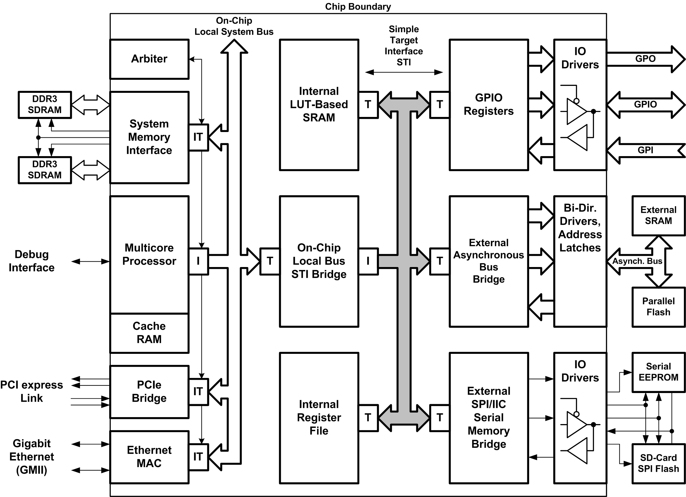
Fig. 1. The place of the STI interface in the volume of the crystal VLSI
The STI interface allows a simple way to connect the functional blocks of a project that do not require the support of the local bus initiator function. The STI protocol makes it possible to read and write data words in each clock cycle, which ensures throughput at the level of a fully functional system bus, with a similar data length and synchronization frequency.
Block transfers of data arrays with the participation of STI artists can be performed by a direct memory access processor (DMA) implemented as part of an STI segment bridge or by other blocks having an initiator connection to a local system bus with access to the STI segment bridge.
Consider the topology of agent communication in the volume of the STI segment.
The STI segment communication uses the signal set shown in Table 1.
Table 1.
For signaling requests for hardware interrupts by STI executors, non-segment-related STI signals can be used, sideband signals, which are controlled by the developer of each individual project.
The topology of logical signal connections in the volume of one STI segment is shown in Fig. 2. In this example, the switching of two performers is presented, as well as the organization of the inputs and outputs of the performers and the initiator. Switching artists performed by dividing the address spaces into two equal parts. Thus, at low level of the high order address S_ADDR [n-1], the performer Target-A is selected, and at high level - Target-B. The logic of the choice of performers can also include the command code for dividing not only by address combinations, but also by address spaces.
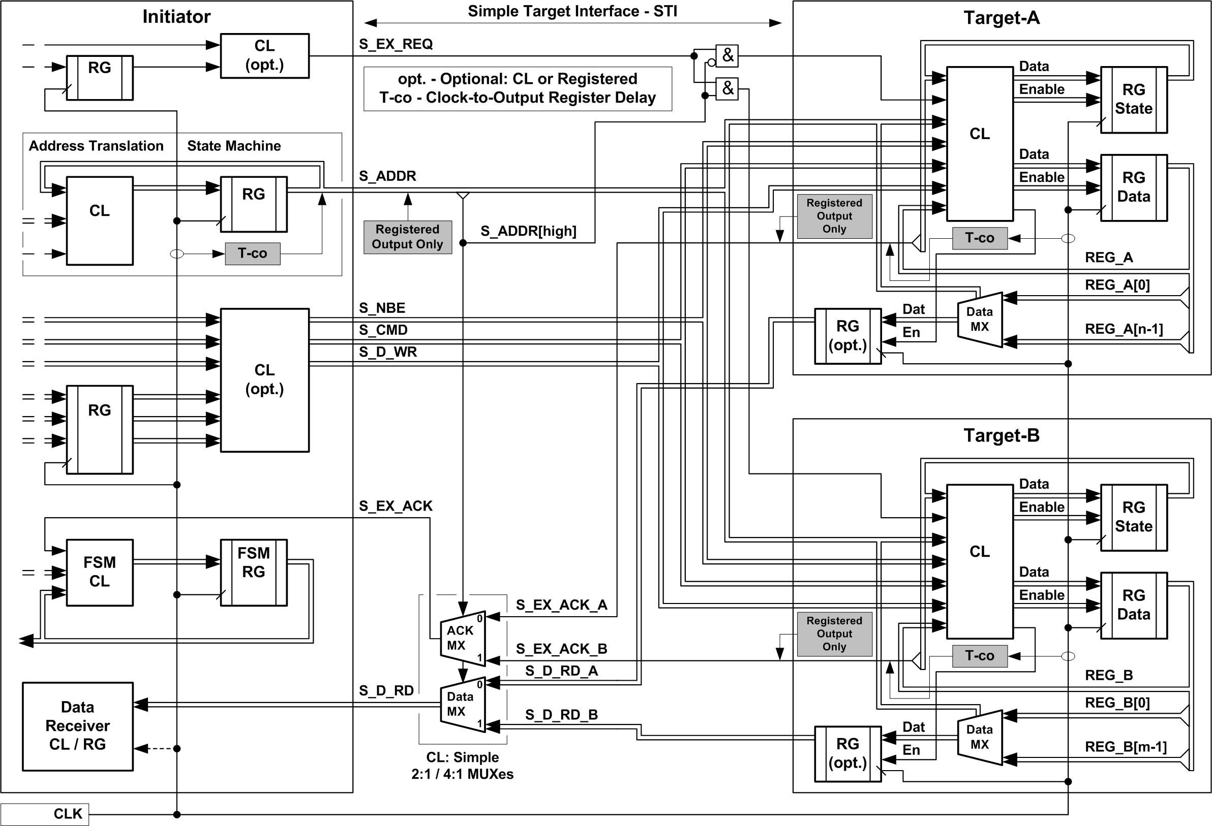
Fig. 2. Connection topology in the STI segment
The following limitations apply to the interface topology of the STI interface initiator:
The following restrictions apply to the topology of the STI interface user interface:
The listed requirements for the topology of the initiator and executor interfaces at the STI junction are caused by the need to exclude the generation of complex combination loops, which significantly complicate the optimization of the project performance and reduce the maximum clock frequency.
Coupling combinational circuits that provide switching of several executors within one STI segment are represented by logic gates “AND” on the S_EX_REQ request circuits as well as by multiplexers of the performers' outputs to the common inputs of the initiator. An example of constructing a cohesive logic is shown in Fig. 2
In a synthesized project model, certain logical signals of an individual STI segment may be absent due to the optimization of combinational logic and the transfer of registers through logical circuits. The results of the synthesis also depend on the user settings specified in the design tools used by the developer (CAD).
Consider the protocol of interaction of agents of one STI segment.
All logical signals of the STI interface, except for the system clock lines CLK and the initial setup (reset) of the RST, must satisfy the requirements of synchronism with respect to the working edge of the clock signal CLK. According to this protocol, the working front is assumed to be ascending, at which a low level is replaced by a high one.
Signal S_NBE carries information about active bytes written or read in the current loop. For an 8-bit STI interface, this signal is not used, because in all cycles no more than one byte is transmitted, which cannot be invalid. An invalid byte on an 8-bit STI segment corresponds to the absence of a loop.
On the 16-bit STI interface, the S_NBE signal is two bits wide. Low level S_NBE [0] signals the validity of data in bits S_D_WR [7: 0] or S_D_RD [7: 0]. A low level of S_NBE [1] signals the presence of valid data in the bits S_D_WR [15: 8] or S_D_RD [15: 8]. A high level of S_NBE [x] indicates a lack of data in the corresponding digits. Thus, these bytes should not be written or considered to be read.
On the 32-bit STI interface, the S_NBE signal is 4 bits wide. Two additional bits S_NBE [3: 2] control the upper half of the data bus. Low level S_NBE [2] signals the validity of data in bits S_D_WR [23:16] or S_D_RD [23:16]. Low level S_NBE [3] indicates the presence of valid data in bits S_D_WR [31:24] or S_D_RD [31:24]. In a similar way, the S_NBE bits [7: 4] control the high bytes of the 64-bit interface, and bit-4 controls byte [39:32], bit-5 controls byte [47:40], bit-6 controls byte [55:48] and bit-7 is the high byte [63:56].
S_CMD [2: 0] lines transmit commands that determine the type of the current exchange cycle. STI commands are listed in Table 2.
Table 2.
The STI interface supports three types of address spaces:
The S_ADDR bus carries an address combination of any of the address spaces. In the 8-bit version of the STI, the low order bit of the address is S_ADDR [0], in the 16-bit version it is designated S_ADDR [1], in the 32-bit version the low-order address is S_ADDR [2], and in the 64-bit version it is S_ADDR [ 3]. This is because the minimum addressable value of the data at the STI junction is byte, and in 16, 32 and 64-bit versions, the low bits of the address S_ADDR [0], S_ADDR [1: 0] and S_ADDR [2: 0], respectively, are replaced positional code sample bytes: S_NBE [1: 0], S_NBE [3: 0] and S_NBE [7: 0].
The S_D_WR bus carries the data words to write and represents the write path.
The S_D_RD bus carries read data words and is a read path.
The loop request signal S_EX_REQ has an active high level and signals the presence or absence of a write or read cycle.
The loop confirmation signal S_EX_ACK is generated by the performer and has an active high level. A low level indicates that the contractor is not ready to accept the data being written or signals that there are no valid read data in the read path.
The exchange cycle at the STI junction is considered complete after fixing the synchronization signal on the working edge of the fact of the simultaneous presence of a high level on the S_EX_REQ and S_EX_ACK lines.
The timing diagram explaining the recording cycle is shown in fig. 3
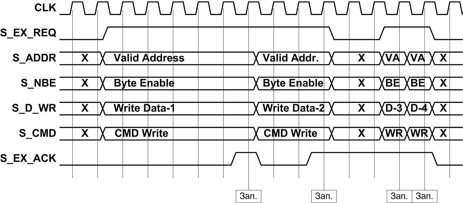
Fig. 3. Example of a timing chart entry
The timing diagram explaining the reading cycle is shown in fig. four.
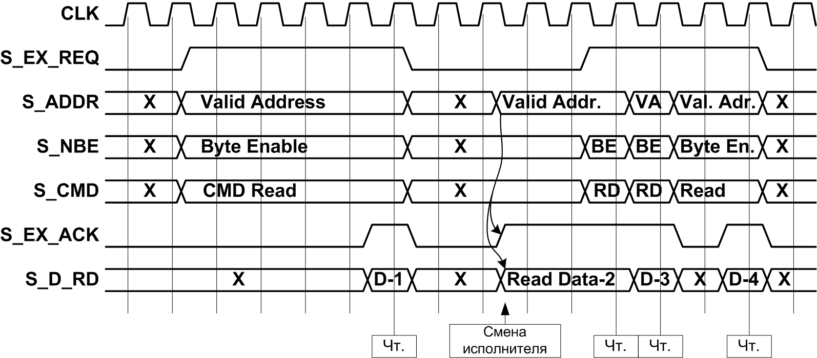
Fig. 4. Example of a temporary reading chart
The procedure for changing the state of signals at the STI interface is governed by the following set of rules.
Rule In-1.
The initiator must provide the actual values of the S_ADDR, S_NBE, S_CMD signals in all clocks in which the loop request is active (high level of the S_EX_REQ signal).
Rule In-2.
The initiator must provide the actual values of the S_D_WR signal in all clocks in which the loop request is active (high level of the S_EX_REQ signal) and a combination of any write command is set on the S_CMD lines.
In-3 rule.
The initiator can change the states of the S_ADDR, S_NBE, S_CMD, S_D_WR signals only during the next clock cycle after simultaneous fixation (on the working edge of the sync signal) of the high level of the S_EX_REQ and S_EX_ACK signals as well as when the S_EX_REQ signal is low.
Rule In-4.
The initiator can set a low level (not to be confused with holding a low level) of the S_EX_REQ signal only during the next clock cycle after simultaneous fixation (on the working edge of the sync signal) of the high level of the S_EX_REQ and S_EX_ACK signals.
Rule Isp-1.
The executor must provide valid read data values on the S_D_RD lines with a high level of the S_EX_ACK loop confirmation signal and the presence of a combination of any read command on the S_CMD lines. (A performer issuing a high level of the S_EX_ACK cycle acknowledgment signal ahead, without waiting for a high level of the S_EX_REQ request signal, should provide the ability to read data when changing the input combinations during one clock cycle before the arrival of the nearest operating edge of the sync signal.)
Rule Isp-2.
The executor must receive and store data for recording from the S_D_WR lines with a high level of the confirmation signal of the S_EX_ACK cycle, a high level at the S_EX_REQ input and a combination of any writing command on the S_CMD lines. (A performer issuing a high level of the S_EX_ACK cycle acknowledgment signal ahead, without waiting for a high level of the S_EX_REQ request signal, should provide the ability to record data when changing the input combinations for one clock cycle until the arrival of the nearest operating edge of the sync signal.)
Rule Is-3.
The executor can set at his output a low level of the cycle confirmation signal S_EX_ACK only during the next clock cycle after simultaneous fixation (on the working edge of the sync signal) of the high level of the signals S_EX_REQ and S_EX_ACK. (The change in the state of the S_EX_ACK signal from low to high, like the diagram in Fig. 4, and from high to low, on the initiator side can be caused by switching of performers by connecting combinational circuits.)
Rule Isp-4.
The contractor may change the state of the signals on the S_D_RD lines only under one of the following conditions:
For clarity, the principles of the internal organization of performers STI consider a few examples of simple functional blocks.
Performers with an STI interface that satisfy all the above rules can be based on simple circuit solutions implemented in any modern element base.
The simplest example of an STI's organization is an I / O expansion unit that implements discrete general-purpose input-outputs (GPIO (General Purpose Input-Output)). A diagram of such a functional block is shown in Fig. five.

Fig. 5. Functional diagram of the I / O expansion unit
This block allows 32 channels to be configured bit by bit for input or output of logic signals. For data, there are two 32-bit registers: RG_O [31: 0] and RG_I [31: 0]. The control is the register RG_T [31: 0], available for reading and writing to the base address (S_ADDR_2 = 0). The RG_I [31: 0] register is available for writing at the address with offset +1 (S_ADDR_2 = 1), the RG_O register [31: 0] is available for reading at the address with +1 offset (S_ADDR_2 = 1).
Writing to registers is done byte-by-byte considering the S_NBE [3: 0] byte resolution combination.
Below is the synthesized model of the considered I / O expansion block, described in the Verilog language:
Another example of an artist is represented by a register file with a capacity of 16 registers with 8 bits. The functional diagram of the register file is shown in Fig. 6
Each of the sixteen registers is available for writing and reading at the STI interface and has an individual output signal RG_xQ [7: 0] used at the top level of the project hierarchy.
The register file is functionally similar to four single-bit distributed memory blocks based on the LUT-4 table converters of the FPGA architecture FPGA (for example, to the RAM16X1D primitives in the FPGA library of Xilinx).
Both considered examples of performers support single-cycle write and read cycles, and therefore, the outputs S_EX_ACK statically give a high level.
The synthesized register file model is described in Verilog as follows:
It is more compact to describe the register file using the spirit of the dimensional array:
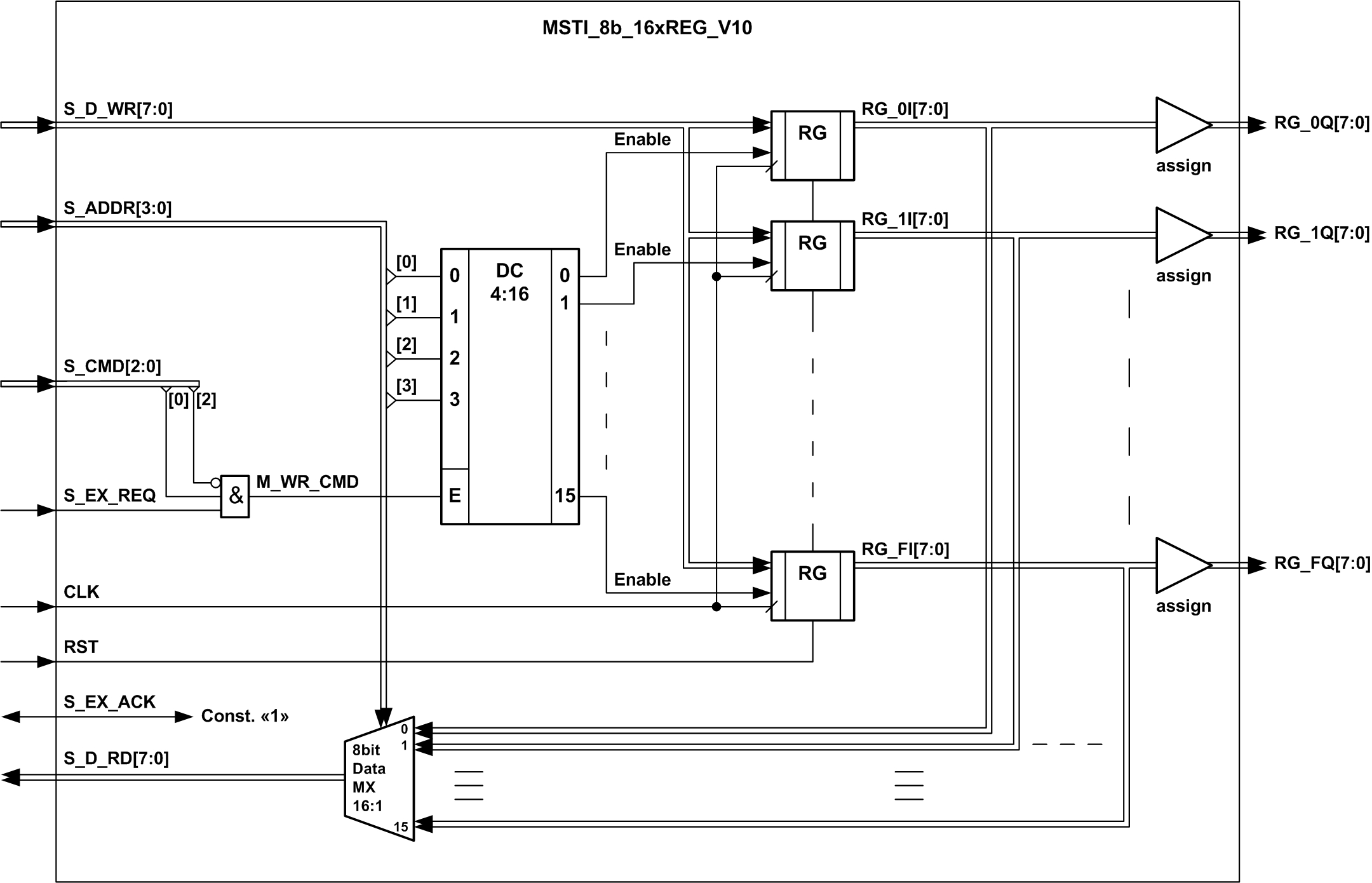
Fig. 6. Functional diagram of the register file
The third example of the STI contractor shows a variant of interfacing with the transmission and reception ports of DTP and DRP data described in [8, 9, 10]. In this example, it became necessary to synthesize a finite state machine that controls the acknowledgment signal of the S_EX_ACK cycle and the internal register busy semaphores.
To transfer bytes to the DTP data transfer port, the buffer register WR_DATA [7: 0] is used, the busy state of which is controlled by the semaphore WR_FULL.
To receive bytes from the DRP data receiving port, the buffer register RD_DATA [7: 0] is used, the occupancy of which is controlled by the semaphore RD_FULL.
Both semaphores are built on identical triggers that operate on the graph shown in the upper left corner of the diagram (Fig. 7). The installation input S1 has a higher priority than the reset input R2. This allows reading from the buffer register in one clock cycle with writing to this register.
The main function of the FSM finite state machine is to set the S_EX_ACK loop confirmation signal at the same time as the read register semaphore is reset, or with the register register semaphore set. The transition graph of the main display automaton below right. The coding of the states of the automaton is chosen in such a way that the output S_EX_ACK is controlled by one of the status bits generated by the current status register.
The remaining outputs of the automaton WR_SET and RD_CLEAR are formed according to Moore's scheme (Moore FSM) with combination elements.
The loop confirmation signal S_EX_ACK is set by the automaton to the active high level in the write cycles upon the fact that the buffer register is empty. In read cycles, the loop confirmation signal S_EX_ACK is set to an active high level as soon as the read buffer register is busy.
The synthesized model of the bridge of interface with the ports of transmission and reception of data, described in the Verilog language, is given below:
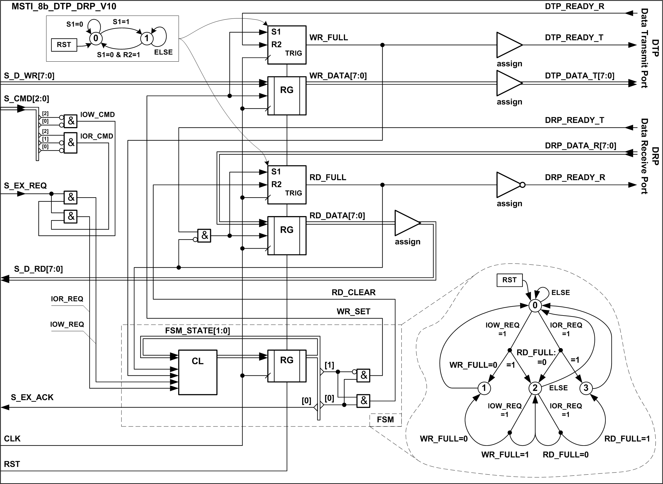
Fig. 7. Functional diagram of the bridge interface STI interface and the ports of transmission and reception of data DTP and DRP
Findings.
A simple STI interface allows you to build performers models for system interfaces of the FPGA configuration project or VLSI chip, providing greater throughput combined with the utmost simplicity of the interaction protocol.
The described interface can be used in peripheral crystal controllers, as well as interfacing bridges with classical exchange channels like I2C, SPI, QSPI, SRAM, FLASH, Microwire and external old-style system buses.
Literature:
1. AMBA APB Protocol. Version: 2.0. Specification. ARM IHI 0024C (ID041610) 2003-2010, ARM.
2. AMBA Specification Rev 2.0. ARM IHI 0011A. ARM Limited 1999.
3. AMBA AXI Protocol. Version: 2.0. Specification. ARM IHI 0022C (ID030510) 2003-2010, ARM.
4. AMBA 4 AXI4-Stream Protocol. Version: 1.0. Specification. ARM IHI 0051A (ID030510). 2010, ARM.
5. WISHBONE System-on-Chip (SoC) Interconnection Architecture for Portable IP Cores. 2010, OpenCores.
6. Open Core Protocol (OCP) Specification Release 2.1. 2005, OCP-IP Association.
7. RTL Hardware Design Using VHDL: Coding for Efficiency, Portability, and Scalability. By Pong P.Chu. John Wiley & Sons, Inc. 2006
8. Borisenko N.V. Approaches to the organization of a unified series of synthesized models of FIFO buffers implemented in various families of programmable logic. Part 1. "Components and technologies" №12.2012.
9. Borisenko N.V. Schemes for including FIFO buffers with a unified interface to the data path between the source and receiver of information. "Components and Technologies" №2.2013.
10. Borisenko N.V. Organization of synchronous FIFO buffers with a unified interface, built on general-purpose registers in the volume of programmable logic chips. "Components and technologies" №8.2016.
Since the semiconductor industry has mastered technological processes with standards of 0.18 micron or less, which have made it possible to achieve the degree of integration of the “System on Crystal” chips, many specifications have appeared on the internal joints of functional units implemented in such chips. In most cases, these junctions are represented by synchronous system buses, such as: AMBA APB, AHB, AXI, Wishbone, OCP [1, 2, 3, 4, 5, 6]. Original topologies have also been proposed that have nothing to do with the bus, for example, on crystal networks - NOC (Networks-On-Chip) [7].
The subject area of this publication is limited to building links of functional blocks of a computing device, without going beyond the VLSI crystal or FPGA. A feature of such connections is the absence of a significant limitation of the number of signal lines involved in the exchange protocol. This feature is due to the fact that the introduction of an additional signal in the crystal volume often significantly simplifies the logic circuits that occupy transistor resources, while the trace resources are not so scarce. It should also be noted that some signals explicitly described in the RTL-level model may be absent in the synthesized scheme and the list of links at the level of technological elements due to the optimization of the combinational logic.
Most of the existing on-chip system bus specifications use complex protocols that define delayed transactions, block transfers (Burst mode), Prefetchable Read, Abort stops, and Retry requests. This functionality requires support from all agents of the bus and leads to a significant complication of switching algorithms for control automata, although in many cases it is not used. In particular, it is redundant in organizing access to slow or simple peripheral crystal blocks.
')
In some specifications, for example, for the Wishbone bus [5], the principle of connecting agents to each other is not regulated, but only the interfaces of the initiator (Initiator) and the performer (Target) are defined.
The main advantage of the existing interfaces is the wide range of developed and verified functional blocks (IP cores).
It is likely that many developers who are accustomed to using standard protocols for crystal system buses, which have been developed in the West for a long time, will have a question: why reinvent the wheel? First, the main purpose of creating a new specification was to describe the simplest synchronous system interface, which regulates all the joints, the internal organization of agents in connection to the bus and the way to build the infrastructure of the bus itself. Secondly, the original specification should be written in Russian, and not in English.
Having defined the objectives of the development and limiting the subject area, we proceed to the direct consideration of the interface specification.
Simple Performer Version 1.0 — Simple Target Interface v.1.0 (hereinafter referred to as STI) is a set of logical signals and an interaction protocol that provides the connection of several functional blocks in a single FPGA configuration project or VLSI chip (hereinafter referred to as the project).
In the RTL model of a project description, there can be an unlimited number of STI interfaces operating in parallel, simultaneously and independently of each other. Each of these interfaces is hereinafter referred to as an STI segment.
The interaction within one STI segment is implemented in one project synchronization domain, which means using a single sync signal (CLK) for the initiator and all performers connected by one STI segment.
The set of functional blocks of the project, connected by a common STI segment, includes one (and only one) initiator of the exchange and a set of executors of the exchange, which are represented by the other blocks of this set.
The STI interaction method consists in writing and reading data words available at certain addresses in one of the processor's address spaces of the computing device. The width of words is determined by the data path width in the interface implementation chosen for a certain STI segment and can be 8, 16, 32 or 64 bits.
Writing or reading a single data word is an exchange cycle over the STI interface (hereinafter referred to as the cycle).
Any STI data exchange begins with a single exchange initiator block in the segment (hereinafter referred to as the initiator). There are several units for executing exchanges (hereinafter referred to as executors) connected to a common STI segment. The maximum number of performers depends on the implementation of the VLSI project by the developer, and is not regulated by this protocol. However, for reasons of speed optimization, it is not recommended to connect more than eight performers to one STI segment. If there are two or more executors on the STI segment, data switching in the read path and control signal switching are performed by connecting combinational circuits. Switching of several executors is made on the basis of the selected address space (STI command), or a selected address range in the volume of the common address space.
In write cycles, data is transmitted from the initiator to the performer, and in read cycles, in the opposite direction. Combined cycles of simultaneous read and write operations are not allowed by this STI protocol.
The choice of address space is encoded in the STI (S_CMD) command. The address in the amount of the selected address space is transmitted from the initiator to the executor in all cycles along the address path (S_ADDR).
The width of the address path depends on the project implementation by the developer, and is not regulated by this protocol. In some functional blocks, the address path at the STI junction may be absent, provided that the contractor is accessed using one combination from the system address space (one register for writing and / or one register for reading).
The location of the STI interface, using the example of a system-on-chip (SBL) class VLSI chip, is illustrated in the block diagram shown in Fig. 1. Links related to the STI segment are highlighted in gray.
Fig. 1. The place of the STI interface in the volume of the crystal VLSI
The STI interface allows a simple way to connect the functional blocks of a project that do not require the support of the local bus initiator function. The STI protocol makes it possible to read and write data words in each clock cycle, which ensures throughput at the level of a fully functional system bus, with a similar data length and synchronization frequency.
Block transfers of data arrays with the participation of STI artists can be performed by a direct memory access processor (DMA) implemented as part of an STI segment bridge or by other blocks having an initiator connection to a local system bus with access to the STI segment bridge.
Consider the topology of agent communication in the volume of the STI segment.
The STI segment communication uses the signal set shown in Table 1.
Table 1.
| 8-p. data paths | 16-p. data paths | 32-p. data paths | 64-p. data paths | Initiator | Executor |
|---|---|---|---|---|---|
| S_EX_REQ | S_EX_REQ | S_EX_REQ | S_EX_REQ | Request output | Request Login |
| S_ADDR [n-1: 0] / S_ADDR_0 | S_ADDR [n-1: 1] / S_ADDR_1 | S_ADDR [n-1: 2] / S_ADDR_2 | S_ADDR [n-1: 3] / S_ADDR_3 | Address output | Address entry |
| not | S_NBE [1: 0] | S_NBE [3: 0] | S_NBE [7: 0] | Byte enable output | Byte enable input |
| S_CMD [2: 0] | S_CMD [2: 0] | S_CMD [2: 0] | S_CMD [2: 0] | Command code output | Command code entry |
| S_D_WR [7: 0] | S_D_WR [15: 0] | S_D_WR [31: 0] | S_D_WR [63: 0] | Write output | Data entry for recording |
| S_EX_ACK | S_EX_ACK | S_EX_ACK | S_EX_ACK | Confirmation login | Confirmation output |
| S_D_RD [7: 0] | S_D_RD [15: 0] | S_D_RD [31: 0] | S_D_RD [63: 0] | Read data input | Read data output |
| CLK | CLK | CLK | CLK | Clock input | Clock input |
| Rst | Rst | Rst | Rst | System reset input | System reset input |
For signaling requests for hardware interrupts by STI executors, non-segment-related STI signals can be used, sideband signals, which are controlled by the developer of each individual project.
The topology of logical signal connections in the volume of one STI segment is shown in Fig. 2. In this example, the switching of two performers is presented, as well as the organization of the inputs and outputs of the performers and the initiator. Switching artists performed by dividing the address spaces into two equal parts. Thus, at low level of the high order address S_ADDR [n-1], the performer Target-A is selected, and at high level - Target-B. The logic of the choice of performers can also include the command code for dividing not only by address combinations, but also by address spaces.
Fig. 2. Connection topology in the STI segment
The following limitations apply to the interface topology of the STI interface initiator:
- The output of the S_ADDR address must have a source in the form of a register output synchronized by the CLK signal. Thus, the delay on the output S_ADDR from the working edge of the clock signal is equal to the output delay of the T-co trigger (Clock-to-Output delay).
- The remaining initiator output signals can be generated by combination circuits that do not react to the input signals S_EX_ACK and S_D_RD, or by registers.
The following restrictions apply to the topology of the STI interface user interface:
- The loop confirmation output S_EX_ACK must have a source in the form of a register output synchronized by the CLK signal. Thus, the delay on the output S_EX_ACK from the working edge of the clock signal is equal to the output delay of the T-co trigger (Clock-to-Output delay). For performers who do not include wait cycles in write exchange cycles and read exchange cycles, it is permissible to form the S_EX_ACK signal as a high-level constant.
- In the absence of an output register on the S_D_RD bus, the multiplexer in the data reading path should be controlled either by the output of the internal register (synchronized by the CLK signal) in the contractor’s volume, or by a subset of the input bits of the S_ADDR address bus [n-1: k].
The listed requirements for the topology of the initiator and executor interfaces at the STI junction are caused by the need to exclude the generation of complex combination loops, which significantly complicate the optimization of the project performance and reduce the maximum clock frequency.
Coupling combinational circuits that provide switching of several executors within one STI segment are represented by logic gates “AND” on the S_EX_REQ request circuits as well as by multiplexers of the performers' outputs to the common inputs of the initiator. An example of constructing a cohesive logic is shown in Fig. 2
In a synthesized project model, certain logical signals of an individual STI segment may be absent due to the optimization of combinational logic and the transfer of registers through logical circuits. The results of the synthesis also depend on the user settings specified in the design tools used by the developer (CAD).
Consider the protocol of interaction of agents of one STI segment.
All logical signals of the STI interface, except for the system clock lines CLK and the initial setup (reset) of the RST, must satisfy the requirements of synchronism with respect to the working edge of the clock signal CLK. According to this protocol, the working front is assumed to be ascending, at which a low level is replaced by a high one.
Signal S_NBE carries information about active bytes written or read in the current loop. For an 8-bit STI interface, this signal is not used, because in all cycles no more than one byte is transmitted, which cannot be invalid. An invalid byte on an 8-bit STI segment corresponds to the absence of a loop.
On the 16-bit STI interface, the S_NBE signal is two bits wide. Low level S_NBE [0] signals the validity of data in bits S_D_WR [7: 0] or S_D_RD [7: 0]. A low level of S_NBE [1] signals the presence of valid data in the bits S_D_WR [15: 8] or S_D_RD [15: 8]. A high level of S_NBE [x] indicates a lack of data in the corresponding digits. Thus, these bytes should not be written or considered to be read.
On the 32-bit STI interface, the S_NBE signal is 4 bits wide. Two additional bits S_NBE [3: 2] control the upper half of the data bus. Low level S_NBE [2] signals the validity of data in bits S_D_WR [23:16] or S_D_RD [23:16]. Low level S_NBE [3] indicates the presence of valid data in bits S_D_WR [31:24] or S_D_RD [31:24]. In a similar way, the S_NBE bits [7: 4] control the high bytes of the 64-bit interface, and bit-4 controls byte [39:32], bit-5 controls byte [47:40], bit-6 controls byte [55:48] and bit-7 is the high byte [63:56].
S_CMD [2: 0] lines transmit commands that determine the type of the current exchange cycle. STI commands are listed in Table 2.
Table 2.
| S_CMD [2] | S_CMD [1] | S_CMD [0] | Cycle type |
|---|---|---|---|
| 0 | 0 | 0 | IO Write - Write IO with the expectation of the final executor (data receiver) |
| 0 | 0 | one | Memory Write - Write to memory with the expectation of the final performer (data receiver) |
| 0 | one | 0 | Posted IO Write - Postponed IO Write |
| 0 | one | one | Posted Memory Write - Postponed write to memory |
| one | 0 | 0 | IO Read - IO reading (without data prefetch) |
| one | 0 | one | Memory Read - Read Memory (without data prefetch) |
| one | one | X | Programm Memory Read - Read program memory (no data prefetch) |
The STI interface supports three types of address spaces:
- IO Space IO Space
- Memory space (or data memory) Memory Space.
- Program memory space (for processor architectures with separate program memory and data) Programm Memory Space.
The S_ADDR bus carries an address combination of any of the address spaces. In the 8-bit version of the STI, the low order bit of the address is S_ADDR [0], in the 16-bit version it is designated S_ADDR [1], in the 32-bit version the low-order address is S_ADDR [2], and in the 64-bit version it is S_ADDR [ 3]. This is because the minimum addressable value of the data at the STI junction is byte, and in 16, 32 and 64-bit versions, the low bits of the address S_ADDR [0], S_ADDR [1: 0] and S_ADDR [2: 0], respectively, are replaced positional code sample bytes: S_NBE [1: 0], S_NBE [3: 0] and S_NBE [7: 0].
The S_D_WR bus carries the data words to write and represents the write path.
The S_D_RD bus carries read data words and is a read path.
The loop request signal S_EX_REQ has an active high level and signals the presence or absence of a write or read cycle.
The loop confirmation signal S_EX_ACK is generated by the performer and has an active high level. A low level indicates that the contractor is not ready to accept the data being written or signals that there are no valid read data in the read path.
The exchange cycle at the STI junction is considered complete after fixing the synchronization signal on the working edge of the fact of the simultaneous presence of a high level on the S_EX_REQ and S_EX_ACK lines.
The timing diagram explaining the recording cycle is shown in fig. 3
Fig. 3. Example of a timing chart entry
The timing diagram explaining the reading cycle is shown in fig. four.
Fig. 4. Example of a temporary reading chart
The procedure for changing the state of signals at the STI interface is governed by the following set of rules.
Rule In-1.
The initiator must provide the actual values of the S_ADDR, S_NBE, S_CMD signals in all clocks in which the loop request is active (high level of the S_EX_REQ signal).
Rule In-2.
The initiator must provide the actual values of the S_D_WR signal in all clocks in which the loop request is active (high level of the S_EX_REQ signal) and a combination of any write command is set on the S_CMD lines.
In-3 rule.
The initiator can change the states of the S_ADDR, S_NBE, S_CMD, S_D_WR signals only during the next clock cycle after simultaneous fixation (on the working edge of the sync signal) of the high level of the S_EX_REQ and S_EX_ACK signals as well as when the S_EX_REQ signal is low.
Rule In-4.
The initiator can set a low level (not to be confused with holding a low level) of the S_EX_REQ signal only during the next clock cycle after simultaneous fixation (on the working edge of the sync signal) of the high level of the S_EX_REQ and S_EX_ACK signals.
Rule Isp-1.
The executor must provide valid read data values on the S_D_RD lines with a high level of the S_EX_ACK loop confirmation signal and the presence of a combination of any read command on the S_CMD lines. (A performer issuing a high level of the S_EX_ACK cycle acknowledgment signal ahead, without waiting for a high level of the S_EX_REQ request signal, should provide the ability to read data when changing the input combinations during one clock cycle before the arrival of the nearest operating edge of the sync signal.)
Rule Isp-2.
The executor must receive and store data for recording from the S_D_WR lines with a high level of the confirmation signal of the S_EX_ACK cycle, a high level at the S_EX_REQ input and a combination of any writing command on the S_CMD lines. (A performer issuing a high level of the S_EX_ACK cycle acknowledgment signal ahead, without waiting for a high level of the S_EX_REQ request signal, should provide the ability to record data when changing the input combinations for one clock cycle until the arrival of the nearest operating edge of the sync signal.)
Rule Is-3.
The executor can set at his output a low level of the cycle confirmation signal S_EX_ACK only during the next clock cycle after simultaneous fixation (on the working edge of the sync signal) of the high level of the signals S_EX_REQ and S_EX_ACK. (The change in the state of the S_EX_ACK signal from low to high, like the diagram in Fig. 4, and from high to low, on the initiator side can be caused by switching of performers by connecting combinational circuits.)
Rule Isp-4.
The contractor may change the state of the signals on the S_D_RD lines only under one of the following conditions:
- after simultaneous fixation (on the working edge of the clock signal) of the high level of the signals S_EX_REQ and S_EX_ACK,
- immediately after changing the state of the S_ADDR address, resolving the S_NBE bytes, or the S_CMD command code until the nearest working edge of the sync signal arrives,
- in cycles with low signal level S_EX_ACK,
- at the same time (in the same cycle) with the installation of a high level at the output S_EX_ACK,
- in cycles, with combinations of S_CMD command codes that do not correspond to read cycles.
For clarity, the principles of the internal organization of performers STI consider a few examples of simple functional blocks.
Performers with an STI interface that satisfy all the above rules can be based on simple circuit solutions implemented in any modern element base.
The simplest example of an STI's organization is an I / O expansion unit that implements discrete general-purpose input-outputs (GPIO (General Purpose Input-Output)). A diagram of such a functional block is shown in Fig. five.
Fig. 5. Functional diagram of the I / O expansion unit
This block allows 32 channels to be configured bit by bit for input or output of logic signals. For data, there are two 32-bit registers: RG_O [31: 0] and RG_I [31: 0]. The control is the register RG_T [31: 0], available for reading and writing to the base address (S_ADDR_2 = 0). The RG_I [31: 0] register is available for writing at the address with offset +1 (S_ADDR_2 = 1), the RG_O register [31: 0] is available for reading at the address with +1 offset (S_ADDR_2 = 1).
Writing to registers is done byte-by-byte considering the S_NBE [3: 0] byte resolution combination.
Below is the synthesized model of the considered I / O expansion block, described in the Verilog language:
`timescale 1ns / 1ps ////////////////////////////////////////////////////////////////////////// // Engineer: FPGA-Mechanic // // Create Date: 11:12:38 07/24/2014 // Design Name: STI Design // Module Name: MSTI_32b_GPIO_REG_V10 - 32-bit STI GPIO Expander // Project Name: Any // Target Devices: FPGA // Tool versions: Xilinx DS 14.4 // // Revision: 1.0 (24.07.2014) // Revision 1.0 - File Created ////////////////////////////////////////////////////////////////////////// module MSTI_32b_GPIO_REG_V10( input CLK, input RST, input S_EX_REQ, input S_ADDR_2, input [3:0] S_NBE, input [2:0] S_CMD, input [31:0] S_D_WR, output S_EX_ACK, output [31:0] S_D_RD, output [31:0] GP_O, output [31:0] GP_T, input [31:0] GP_I ); // Internal signals declaration: wire IO_WR_CMD; reg [31:0] RG_T, RG_O, RG_I; //------------------------------------------ assign IO_WR_CMD = ~S_CMD[0] & ~S_CMD[2] & S_EX_REQ; //------------------------------------------ // Internal Data Registers: always @ (posedge CLK, posedge RST) if(RST) begin RG_T <= 32'hFFFFFFFF; // All Outputs Tri-Stated RG_O <= 32'h00000000; RG_I <= 32'h00000000; end else begin RG_I <= GP_I; if(~S_NBE[0] & ~S_ADDR_2 & IO_WR_CMD) RG_T[7:0] <= S_D_WR[7:0]; if(~S_NBE[1] & ~S_ADDR_2 & IO_WR_CMD) RG_T[15:8] <= S_D_WR[15:8]; if(~S_NBE[2] & ~S_ADDR_2 & IO_WR_CMD) RG_T[23:16] <= S_D_WR[23:16]; if(~S_NBE[3] & ~S_ADDR_2 & IO_WR_CMD) RG_T[31:24] <= S_D_WR[31:24]; if(~S_NBE[0] & S_ADDR_2 & IO_WR_CMD) RG_O[7:0] <= S_D_WR[7:0]; if(~S_NBE[1] & S_ADDR_2 & IO_WR_CMD) RG_O[15:8] <= S_D_WR[15:8]; if(~S_NBE[2] & S_ADDR_2 & IO_WR_CMD) RG_O[23:16] <= S_D_WR[23:16]; if(~S_NBE[3] & S_ADDR_2 & IO_WR_CMD) RG_O[31:24] <= S_D_WR[31:24]; end //------------------------------------------ assign S_EX_ACK = 1'b1; //------------------------------------------ assign GP_T = RG_T; assign GP_O = RG_O; //------------------------------------------ assign S_D_RD = S_ADDR_2 ? RG_I : RG_T; //------------------------------------------ endmodule Another example of an artist is represented by a register file with a capacity of 16 registers with 8 bits. The functional diagram of the register file is shown in Fig. 6
Each of the sixteen registers is available for writing and reading at the STI interface and has an individual output signal RG_xQ [7: 0] used at the top level of the project hierarchy.
The register file is functionally similar to four single-bit distributed memory blocks based on the LUT-4 table converters of the FPGA architecture FPGA (for example, to the RAM16X1D primitives in the FPGA library of Xilinx).
Both considered examples of performers support single-cycle write and read cycles, and therefore, the outputs S_EX_ACK statically give a high level.
The synthesized register file model is described in Verilog as follows:
`timescale 1ns / 1ps ////////////////////////////////////////////////////////////////////////// // Engineer: FPGA-Mechanic // // Create Date: 11:40:08 07/24/2014 // Design Name: STI Design // Module Name: MSTI_8b_16xREG_V10 - 16x8bit Register File // in STI Memory Space // Project Name: Any // Target Devices: FPGA // Tool versions: Xilinx DS 14.4 // // Revision: 1.0 (24.07.2014) // Revision 1.0 - File Created ////////////////////////////////////////////////////////////////////////// module MSTI_8b_16xREG_V10( input CLK, input RST, input S_EX_REQ, input [3:0] S_ADDR, //input [1:0] S_NBE, input [2:0] S_CMD, input [7:0] S_D_WR, output S_EX_ACK, output reg [7:0] S_D_RD, output [7:0] RG_0Q, output [7:0] RG_1Q, output [7:0] RG_2Q, output [7:0] RG_3Q, output [7:0] RG_4Q, output [7:0] RG_5Q, output [7:0] RG_6Q, output [7:0] RG_7Q, output [7:0] RG_8Q, output [7:0] RG_9Q, output [7:0] RG_AQ, output [7:0] RG_BQ, output [7:0] RG_CQ, output [7:0] RG_DQ, output [7:0] RG_EQ, output [7:0] RG_FQ ); // Internal signals declaration: wire M_WR_CMD; reg [7:0] RG_0I, RG_1I, RG_2I, RG_3I, RG_4I, RG_5I, RG_6I, RG_7I; reg [7:0] RG_8I, RG_9I, RG_AI, RG_BI, RG_CI, RG_DI, RG_EI, RG_FI; //------------------------------------------ assign M_WR_CMD = ~S_CMD[2] & S_CMD[0] & S_EX_REQ; //------------------------------------------ // Internal Data Registers: always @ (posedge CLK, posedge RST) if(RST) begin RG_0I <= 8'h00; RG_1I <= 8'h00; RG_2I <= 8'h00; RG_3I <= 8'h00; RG_4I <= 8'h00; RG_5I <= 8'h00; RG_6I <= 8'h00; RG_7I <= 8'h00; RG_8I <= 8'h00; RG_9I <= 8'h00; RG_AI <= 8'h00; RG_BI <= 8'h00; RG_CI <= 8'h00; RG_DI <= 8'h00; RG_EI <= 8'h00; RG_FI <= 8'h00; end else begin if(M_WR_CMD) case(S_ADDR) 4'h0 : RG_0I <= S_D_WR; 4'h1 : RG_1I <= S_D_WR; 4'h2 : RG_2I <= S_D_WR; 4'h3 : RG_3I <= S_D_WR; 4'h4 : RG_4I <= S_D_WR; 4'h5 : RG_5I <= S_D_WR; 4'h6 : RG_6I <= S_D_WR; 4'h7 : RG_7I <= S_D_WR; 4'h8 : RG_8I <= S_D_WR; 4'h9 : RG_9I <= S_D_WR; 4'hA : RG_AI <= S_D_WR; 4'hB : RG_BI <= S_D_WR; 4'hC : RG_CI <= S_D_WR; 4'hD : RG_DI <= S_D_WR; 4'hE : RG_EI <= S_D_WR; default: RG_FI <= S_D_WR; endcase end //------------------------------------------ // Output MUX: always @ (S_ADDR, RG_0I, RG_1I, RG_2I, RG_3I, RG_4I, RG_5I, RG_6I, RG_7I, RG_8I, RG_9I, RG_AI, RG_BI, RG_CI, RG_DI, RG_EI, RG_FI) case(S_ADDR) 4'h0 : S_D_RD <= RG_0I; 4'h1 : S_D_RD <= RG_1I; 4'h2 : S_D_RD <= RG_2I; 4'h3 : S_D_RD <= RG_3I; 4'h4 : S_D_RD <= RG_4I; 4'h5 : S_D_RD <= RG_5I; 4'h6 : S_D_RD <= RG_6I; 4'h7 : S_D_RD <= RG_7I; 4'h8 : S_D_RD <= RG_8I; 4'h9 : S_D_RD <= RG_9I; 4'hA : S_D_RD <= RG_AI; 4'hB : S_D_RD <= RG_BI; 4'hC : S_D_RD <= RG_CI; 4'hD : S_D_RD <= RG_DI; 4'hE : S_D_RD <= RG_EI; default: S_D_RD <= RG_FI; endcase //------------------------------------------ assign S_EX_ACK = 1'b1; //------------------------------------------ // Regs Outputs: assign RG_0Q = RG_0I; assign RG_1Q = RG_1I; assign RG_2Q = RG_2I; assign RG_3Q = RG_3I; assign RG_4Q = RG_4I; assign RG_5Q = RG_5I; assign RG_6Q = RG_6I; assign RG_7Q = RG_7I; assign RG_8Q = RG_8I; assign RG_9Q = RG_9I; assign RG_AQ = RG_AI; assign RG_BQ = RG_BI; assign RG_CQ = RG_CI; assign RG_DQ = RG_DI; assign RG_EQ = RG_EI; assign RG_FQ = RG_FI; //------------------------------------------ endmodule It is more compact to describe the register file using the spirit of the dimensional array:
`timescale 1ns / 1ps ////////////////////////////////////////////////////////////////////////// // Engineer: FPGA-Mechanic // // Create Date: 11:40:08 07/24/2014 // Design Name: STI Design // Module Name: MSTI_8b_16xREG_V11 - 16x8bit Register File // in STI Memory Space // Project Name: Any // Target Devices: FPGA // Tool versions: Xilinx DS 14.4 // // Revision: 1.1 (24.07.2014) Array Coding // Revision 1.0 - File Created ////////////////////////////////////////////////////////////////////////// module MSTI_8b_16xREG_V11( input CLK, input RST, input S_EX_REQ, input [3:0] S_ADDR, //input [1:0] S_NBE, input [2:0] S_CMD, input [7:0] S_D_WR, output S_EX_ACK, output [7:0] S_D_RD, output [7:0] RG_0Q, output [7:0] RG_1Q, output [7:0] RG_2Q, output [7:0] RG_3Q, output [7:0] RG_4Q, output [7:0] RG_5Q, output [7:0] RG_6Q, output [7:0] RG_7Q, output [7:0] RG_8Q, output [7:0] RG_9Q, output [7:0] RG_AQ, output [7:0] RG_BQ, output [7:0] RG_CQ, output [7:0] RG_DQ, output [7:0] RG_EQ, output [7:0] RG_FQ ); // Internal signals declaration: wire M_WR_CMD; reg [7:0] RG_I [15:0]; // Array 16 x 8bit //------------------------------------------ assign M_WR_CMD = ~S_CMD[2] & S_CMD[0] & S_EX_REQ; //------------------------------------------ // Internal Data Registers: always @ (posedge CLK, posedge RST) if(RST) begin RG_I[0] <= 8'h00; RG_I[1] <= 8'h00; RG_I[2] <= 8'h00; RG_I[3] <= 8'h00; RG_I[4] <= 8'h00; RG_I[5] <= 8'h00; RG_I[6] <= 8'h00; RG_I[7] <= 8'h00; RG_I[8] <= 8'h00; RG_I[9] <= 8'h00; RG_I[4'hA] <= 8'h00; RG_I[4'hB] <= 8'h00; RG_I[4'hC] <= 8'h00; RG_I[4'hD] <= 8'h00; RG_I[4'hE] <= 8'h00; RG_I[4'hF] <= 8'h00; end else if(M_WR_CMD) RG_I[S_ADDR] <= S_D_WR; //------------------------------------------ // Output MUX: assign S_D_RD = RG_I[S_ADDR]; //------------------------------------------ assign S_EX_ACK = 1'b1; //------------------------------------------ // Regs Outputs: assign RG_0Q = RG_I[0]; assign RG_1Q = RG_I[1]; assign RG_2Q = RG_I[2]; assign RG_3Q = RG_I[3]; assign RG_4Q = RG_I[4]; assign RG_5Q = RG_I[5]; assign RG_6Q = RG_I[6]; assign RG_7Q = RG_I[7]; assign RG_8Q = RG_I[8]; assign RG_9Q = RG_I[9]; assign RG_AQ = RG_I[4'hA]; assign RG_BQ = RG_I[4'hB]; assign RG_CQ = RG_I[4'hC]; assign RG_DQ = RG_I[4'hD]; assign RG_EQ = RG_I[4'hE]; assign RG_FQ = RG_I[4'hF]; //------------------------------------------ endmodule Fig. 6. Functional diagram of the register file
The third example of the STI contractor shows a variant of interfacing with the transmission and reception ports of DTP and DRP data described in [8, 9, 10]. In this example, it became necessary to synthesize a finite state machine that controls the acknowledgment signal of the S_EX_ACK cycle and the internal register busy semaphores.
To transfer bytes to the DTP data transfer port, the buffer register WR_DATA [7: 0] is used, the busy state of which is controlled by the semaphore WR_FULL.
To receive bytes from the DRP data receiving port, the buffer register RD_DATA [7: 0] is used, the occupancy of which is controlled by the semaphore RD_FULL.
Both semaphores are built on identical triggers that operate on the graph shown in the upper left corner of the diagram (Fig. 7). The installation input S1 has a higher priority than the reset input R2. This allows reading from the buffer register in one clock cycle with writing to this register.
The main function of the FSM finite state machine is to set the S_EX_ACK loop confirmation signal at the same time as the read register semaphore is reset, or with the register register semaphore set. The transition graph of the main display automaton below right. The coding of the states of the automaton is chosen in such a way that the output S_EX_ACK is controlled by one of the status bits generated by the current status register.
The remaining outputs of the automaton WR_SET and RD_CLEAR are formed according to Moore's scheme (Moore FSM) with combination elements.
The loop confirmation signal S_EX_ACK is set by the automaton to the active high level in the write cycles upon the fact that the buffer register is empty. In read cycles, the loop confirmation signal S_EX_ACK is set to an active high level as soon as the read buffer register is busy.
The synthesized model of the bridge of interface with the ports of transmission and reception of data, described in the Verilog language, is given below:
`timescale 1ns / 1ps ////////////////////////////////////////////////////////////////////////// // Engineer: FPGA-Mechanic // // Create Date: 12:37:39 07/24/2014 // Design Name: STI Design // Module Name: MSTI_8b_DTP_DRP_V10 8-bit STI to DTP & DRP Bridge // Project Name: Any // Target Devices: FPGA // Tool versions: Xilinx DS 14.4 // // Revision: 1.0 (24.07.2014) // Revision 1.0 - File Created ////////////////////////////////////////////////////////////////////////// module MSTI_8b_DTP_DRP_V10( input CLK, input RST, input S_EX_REQ, //input S_ADDR_0, //input [1:0] S_NBE, input [2:0] S_CMD, input [7:0] S_D_WR, output S_EX_ACK, output [7:0] S_D_RD, output DTP_READY_T, output [7:0] DTP_DATA_T, input DTP_READY_R, input DRP_READY_T, input [7:0] DRP_DATA_R, output DRP_READY_R ); // Internal signals declaration: wire IOW_CMD, IOR_CMD; wire IOW_REQ, IOR_REQ; reg [7:0] WR_DATA, RD_DATA; reg WR_FULL, RD_FULL; reg [1:0] FSM_STATE; wire WR_SET, RD_CLEAR; //------------------------------------------ assign IOW_CMD = ~S_CMD[0] & ~S_CMD[2]; assign IOR_CMD = ~S_CMD[0] & ~S_CMD[1] & S_CMD[2]; assign IOW_REQ = IOW_CMD & S_EX_REQ; assign IOR_REQ = IOR_CMD & S_EX_REQ; //------------------------------------------ // Internal Data Registers: always @ (posedge CLK, posedge RST) if(RST) begin WR_DATA <= 8'h00; RD_DATA <= 8'h00; end else begin if(WR_SET) WR_DATA <= S_D_WR; if(~RD_FULL & DRP_READY_T) RD_DATA <= DRP_DATA_R; end assign S_D_RD = RD_DATA; assign DTP_DATA_T = WR_DATA; //------------------------------------------ // Internal Data Semaphores: always @ (posedge CLK, posedge RST) if(RST) begin WR_FULL <= 1'b0; RD_FULL <= 1'b0; end else begin if(WR_SET) WR_FULL <= 1'b1; else if(DTP_READY_R) WR_FULL <= 1'b0; if(~RD_FULL & DRP_READY_T) RD_FULL <= 1'b1; else if(RD_CLEAR) RD_FULL <= 1'b0; end assign DTP_READY_T = WR_FULL; assign DRP_READY_R = ~RD_FULL; //------------------------------------------ // Finite State Machine: always @ (posedge CLK, posedge RST) if(RST) FSM_STATE <= 2'd0; else begin case(FSM_STATE) 2'd0 : if(IOW_REQ) if(WR_FULL) FSM_STATE <= 2'd2; else FSM_STATE <= 2'd1; else if(IOR_REQ) if(RD_FULL) FSM_STATE <= 2'd3; else FSM_STATE <= 2'd2; else FSM_STATE <= 2'd0; 2'd1 : FSM_STATE <= 2'd0; 2'd2 : if(IOW_REQ) if(WR_FULL) FSM_STATE <= 2'd2; else FSM_STATE <= 2'd1; else if(IOR_REQ) if(RD_FULL) FSM_STATE <= 2'd3; else FSM_STATE <= 2'd2; else FSM_STATE <= 2'd0; default: FSM_STATE <= 2'd0; endcase end //------------------------------------------ // Moore Outputs assign WR_SET = ~FSM_STATE[1] & FSM_STATE[0]; assign RD_CLEAR = &(FSM_STATE); //------------------------------------------ assign S_EX_ACK = FSM_STATE[0]; //------------------------------------------ endmodule Fig. 7. Functional diagram of the bridge interface STI interface and the ports of transmission and reception of data DTP and DRP
Findings.
A simple STI interface allows you to build performers models for system interfaces of the FPGA configuration project or VLSI chip, providing greater throughput combined with the utmost simplicity of the interaction protocol.
The described interface can be used in peripheral crystal controllers, as well as interfacing bridges with classical exchange channels like I2C, SPI, QSPI, SRAM, FLASH, Microwire and external old-style system buses.
Literature:
1. AMBA APB Protocol. Version: 2.0. Specification. ARM IHI 0024C (ID041610) 2003-2010, ARM.
2. AMBA Specification Rev 2.0. ARM IHI 0011A. ARM Limited 1999.
3. AMBA AXI Protocol. Version: 2.0. Specification. ARM IHI 0022C (ID030510) 2003-2010, ARM.
4. AMBA 4 AXI4-Stream Protocol. Version: 1.0. Specification. ARM IHI 0051A (ID030510). 2010, ARM.
5. WISHBONE System-on-Chip (SoC) Interconnection Architecture for Portable IP Cores. 2010, OpenCores.
6. Open Core Protocol (OCP) Specification Release 2.1. 2005, OCP-IP Association.
7. RTL Hardware Design Using VHDL: Coding for Efficiency, Portability, and Scalability. By Pong P.Chu. John Wiley & Sons, Inc. 2006
8. Borisenko N.V. Approaches to the organization of a unified series of synthesized models of FIFO buffers implemented in various families of programmable logic. Part 1. "Components and technologies" №12.2012.
9. Borisenko N.V. Schemes for including FIFO buffers with a unified interface to the data path between the source and receiver of information. "Components and Technologies" №2.2013.
10. Borisenko N.V. Organization of synchronous FIFO buffers with a unified interface, built on general-purpose registers in the volume of programmable logic chips. "Components and technologies" №8.2016.
Source: https://habr.com/ru/post/354818/
All Articles