ECO Flow in Vivado or working in netlist editing mode
annotation
The article describes the mode of operation of Vivado, which allows you to make changes to the project at the level of editing the netlist (hereinafter referred to as netlist). Both the ECO mode itself and some nuances that appear while working in it are described. A demo is given and a complete sequence of actions is described for obtaining a result, which anyone who is willing to be able to make sure of its efficiency. The article will be useful for "common development" for FPGA developers, and especially for those who often debug projects in the Logic Analyzer. I hope that work in this mode will be of interest to developers working with large crystals, the compilation time in which can reach hours (or even tens of hours), because in this mode the time spent on implementation can be reduced to literally a couple of minutes.

Table of contents
- annotation
- Introduction
- 1. ECO: an overview
- 2. Design Checkpoint
- 3. Development of a test project
- 3.1. Project creation
- 3.2. Creating and adding HDL files to the project
- 3.3. Creating a MicroBlaze project and working in IP Integrator
- 3.4.Synthesis and implementation
- 3.5. Writing a program for MicroBlaze
- 3.6.Starting and debugging
- 4. Transition to ECO mode
- 5. ECO: interface description
- 6. Making changes to the project
- 6.1. Creating new items in a netlist
- 6.2. Change of properties / parameters of components
- 6.3. Connecting other circuits to probes and ILA
- 6.4. Replacing I / O Ports
- 7. Comparative analysis
- 8. Conclusion
- 9. Homework
- Bibliographic list
The article has a lot of pictures not in the spoilers (140 pieces). Please be careful if you are logging in from the phone.
Introduction
Often, when I have to give a lecture or conduct a seminar, I always try to tell a little more than the program suggests. So it was in the last three seminars devoted to working with single-core Zynq-7000S. This time it was interesting to see how the audience knows about some of the “hidden” modes of work with Vivado. The question was quite simple: “Does any of those present know about the ECO Flow mode?” Immediately after the question was followed, as they say, “a forest of hands, to which I was not particularly surprised.
')
The desire to enlighten the developers at least about the availability of this mode in Vivado, not to mention the demonstration of work in it, appeared to me for a very long time. But for some mysterious reason, I “harnessed” to writing guidelines for building projects using MicroBlaze and working with it. However, after recent seminars, it became obvious that it was still necessary to write about ECO Flow.
The purpose of the article is to give a general idea of the ECO mode in the Vivado environment [1] provided by Xilinx for its crystals and show with a real example the work in this mode, trying to point out the “subtle” moments and analyze its advantages and disadvantages.
The tasks that are set in this article:
- develop a test case that, whenever possible, contains and demonstrates all (or at least most) of the capabilities of working in ECO mode
- implement the project;
- explain the concept of Design Checkpoint;
- describe the transition to the ECO mode of operation;
- edit the netlist and get the FPGA firmware file;
- make sure the changes are correct;
- create a summary table of time spent on standard changes to the project and compare it with the time spent in ECO mode, as well as incremental implementation.
Unfortunately, physically checking the methodology on a rather “heavy” crystal (for example, Virtex UltraScale) is not possible for me. But, I think, even the example that will be given - with a test on the modest Artix-7 installed on the Arty [2] board, will be quite revealing. In the process of writing, I will rely on several basic documents that describe the ECO mode [3], [4], [5]. The used version of Vivado (and, accordingly, the documentation) - 2017.4.
A small digression: yes, in the manual there are a lot of pictures and “trivialities” on how to create a project, build a processor system on MicroBlaze, work in IP Integrator, debug, etc. If you are experienced and just want to read about ECO - please go directly to chapter 4: “Switching to ECO mode” . If you don’t know how to build a project on MicroBlaze, you have never worked at IP Integrator, or you like guides in the style of step-by-step illustrations, I’ll only be happy if you take an additional 75-90 minutes to the presented material. And yet, I hope that someone will execute the manual completely, with a check in the gland.
1. ECO: an overview
ECO - Engineering change orders [6] (“procedure for making engineering changes”) is a mode in which it is possible to make changes to a netlist, a synthesized or implemented project with minimal impact on the original netlist. Vivado has an ECO mode in which it is possible to change the so-called Design Checkpoint project (see below), implement the changes made, generate the necessary reports for the changed netlist and generate the FPGA firmware file on it.
The most typical application of this mode:
- Modification of probes and connected lines of logic analyzers (ILA - IntegratedLogicAnalyzer) when debugging a project. The user can change the set of lines connected to ILA, while avoiding complete re-implementation of the project.
- Reassignment of the chains connected to the FPGA legs. In case the project developer, circuit designer, or circuit board developer made an error in assigning the legs (for example, rx was confused with tx), and the project on the FPGA was already implemented, this way you can reassign ports in the netlist, avoiding repeated full implementation (t . e. synthesis, mapping, optimization, placement, tracing - with all the attendant costs of machine time and resources) of the project.
- Performing “what_ if?” Analysis (editing the contents of the memory, changing the functionality of the LUT, improving the timings, etc.)
The main task of working in ECO mode is to save time and avoid re-implementation of the project when making changes during the project setup or debugging phase. Many people are familiar with the incremental implementation mode, which is also used in ECO, but in ECO, compared to incremental implementation, it is faster to get the firmware file and to perform the current iteration of debugging faster.
Note: working in ECO mode is only possible with Design Checkpoint.
2. Design Checkpoint
The design route is divided into several components:, including synthesis and implementation. The implementation in turn is divided into sub-steps: various optimizations, placement and tracing. The intermediate stages of the design route are stored in a “container”, called Design Checkpoint (DCP) [7]. This is a file with the extension ".dcp". Design Checkpoint contains:
- The current netlist (depending on the stage of the design route), including all the optimizations performed before recording the dcp file.
- The constraints imposed on the project (design constraints).
By default, Vivado creates four dcp files: one - at the stage of synthesis of the module of the top level of the project (if synthesis is performed in out-of-context mode, then for all modules that are synthesized in out-of-context, a dcp file is created) and three - at the implementation stage. These files can be found in folders:
"Project_name.runs / synthesis_name / module_top_name.dcp"
"Project_name.runs / impementionation_name /".
In fig. Figure 1 shows an example of the location and .dcp files that are created by default for some abstract project.
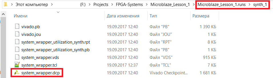
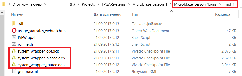
Figure 1 - the default dcp files (1 - “postsynthesis-” and 3 - “postimplement-”: after optimization (_opt), after placement (_placed) and after tracing (_routed))
In Vivado project mode (Project Mode [8]), .dcp files are created automatically. But when working in non-project mode (Non-ProjectMode [8]), the user must ensure that the “snapshots” of the current state of the project are recorded. To do this, use the appropriate Tcl commands [9, 10] .:
write_checkpoint <file_name>.dcp read_checkpoint <file_name>.dcp About why, how and what files dcp should be opened, will be discussed below.
3. Development of a test project
To demonstrate ECO capabilities on a test project, it should contain the following:
- Elements that are not in the original netlist or elements for which you can change the functionality. For example, to start the LED on the button - and in the original project it will light up on pressing, and in the modified one - on pressing it will go out. That is, you will need to add an inverter to the netlist that is not in the original project.
- Items that you can change the content. For example, the truth table in the LUT or the contents of the block memory. And the change in the contents of the block memory will be more preferable here, since we will already perform the change in LUT in claim 1, when we create an additional inverter.
- ILA - to be able to replace connected circuits with other circuits. That is, without touching ILA itself, we will try to replace the selected circuits connected to it in the initial project with others through a netlist.
- Confused conclusions. Suppose that when designing a printed circuit board, the developer performed the pin-swap of two pins for easy wiring, without agreeing with the FPGA developer, i.e. made a mistake of confusing rx with tx UART. In ECO mode, we will have to restore the correct connection.
3.1. Project creation
Find the Vivado icon and double-click on it, a welcome window will open (fig. 2)
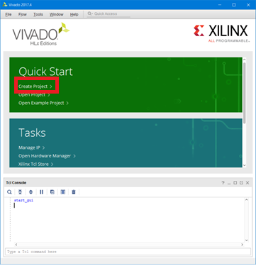
Figure 2 - Vivado Welcome Window
To create a new project, click the Create Project button. Pressing the button calls the wizard to create a new project. After its appearance, click the Next button (Fig. 3).
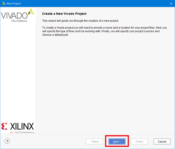
Figure 3 - New project wizard window
Enter the name of the project, in the Project Name field we write “eco_flow”. Specify where the project will be located: in the Project location field specify the directory with the project. I will have it “F: / Projects / FPGA-Systems / eco_flow / projects / vivado”. If you check the “create project subdirectory” checkbox, an additional folder with the project name will be created. Click Next (fig. 4).

Figure 4 - Entering the name of the project and its location
We create an ordinary project, so we simply select the type of project RTL. At the current stage, we will not add any files to the project, so we’ll check the box “Do not specify sources at this time” and click Next (Fig. 5).
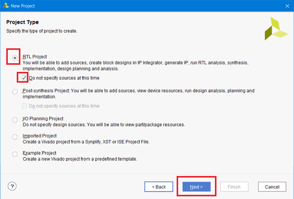
Figure 5 - Selecting the type of project being created
We will work with the Arty board [2], so we will choose the crystal that is installed on it: xc7a35tcsg324-1. Click Next (fig. 6).
Note: I do not specifically choose a ready board from a template of available boards. This is done so that you can manually make mistakes, which we will fix later.

Figure 6 - Crystal Selection xc7a35tcsg324-1
The final in the New Project Setup Wizard will be the Summary window of the project being created. Click Finish (Fig. 7).
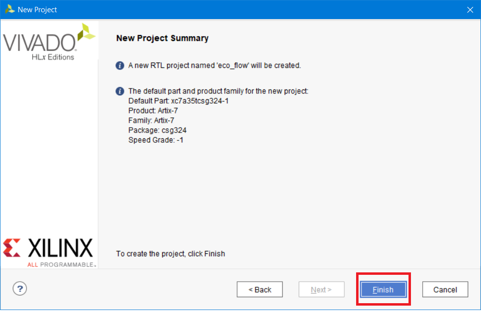
Figure 7 - The brief information window of the project being created
3.2. Creating and adding HDL files to the project
Here we will create two modules: just a flashing LED and a block memory, which is constantly read (in fact, this is an imitation of the memory of filter coefficients, the values of which we later try to change).
To create and add a new file to the project, use the wizard, which is called by pressing the blue plus (Fig. 8).
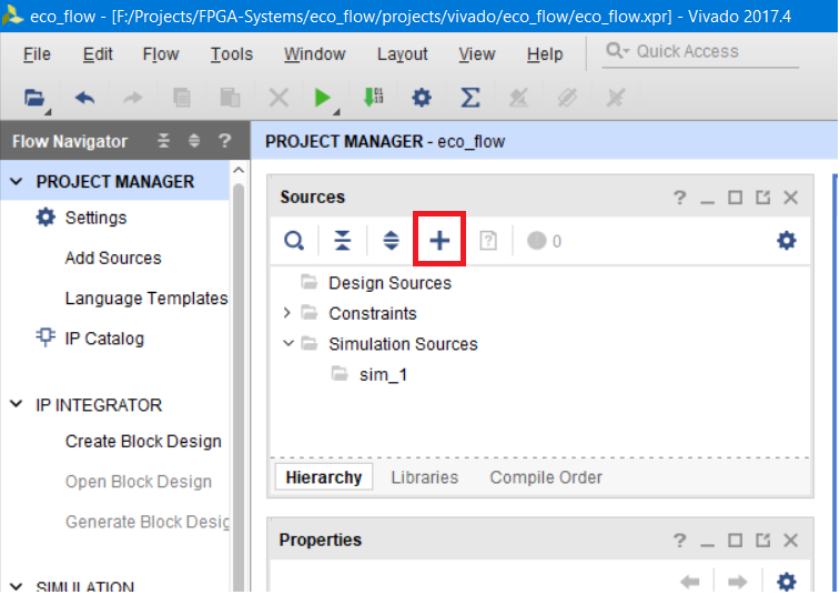
Figure 8 - Calling the Create New Files Wizard
In the window that appears, select "Add or create design sources" and click Next (Fig. 9).
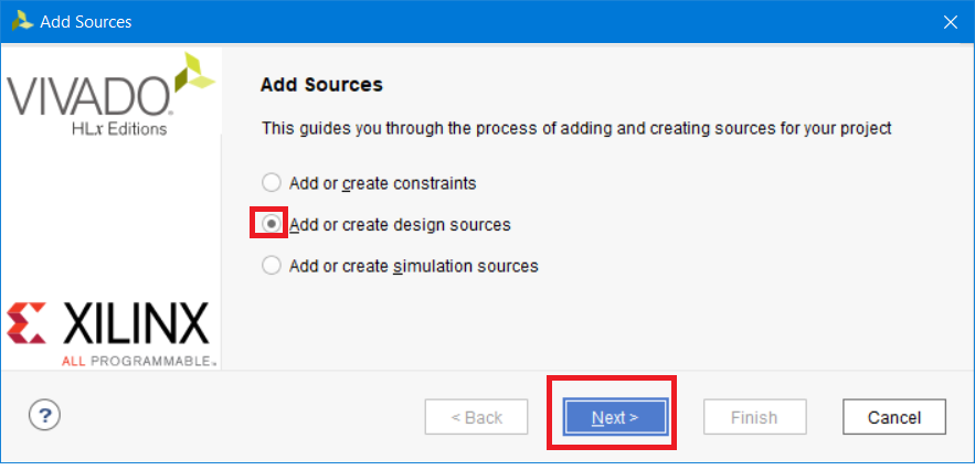
Figure 9 - Selecting the type of file being created or added
Select Create file, then in the window that appears in the File name field, enter the name of the flash_led file to be created, click OK (Fig. 10).
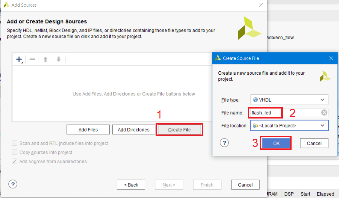
Figure 10 - Creating a new file and entering its name
After that, the file will appear in the list of entries. Click Finish (Fig. 11)
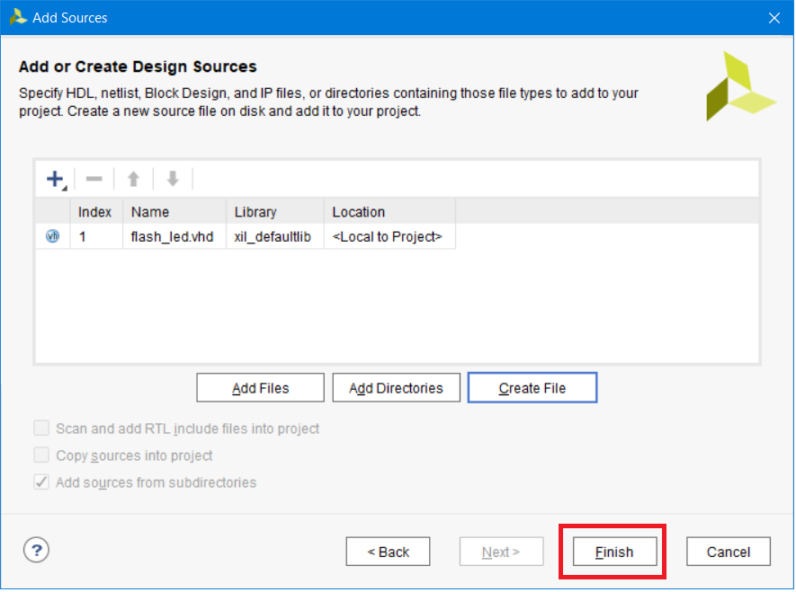
Figure 11 - List of added or created files
Now the wizard to create a template for the file. Since I use VHDL, I can change the architecture name to rtl. We create two pins of our module: iclk with the “in” direction (clock signal of our module) and oled with the “out” direction (output connected to the LED). Click OK (Fig. 12).
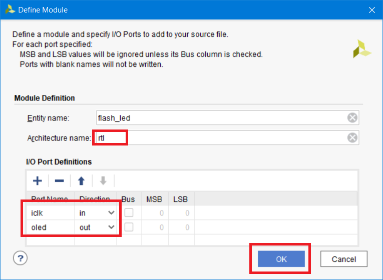
Figure 12 - Module Template Creation Wizard (for VHDL)
Now our module is in the project tree (Fig. 13).
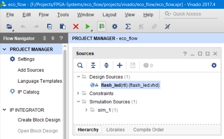
Figure 13 - The created flash_led module
The module should perform a simple function: just blink the LED with a period of 1 second. Looking ahead, I will say that the clock frequency of our project will be equal to 100 MHz, and the module itself will still be useful for you when doing homework.
Replace the contents of the file with the following (Listing 1 (text version of listing 1 see Appendix A)). The code is quite simple, and does not require additional comments to explain its work.
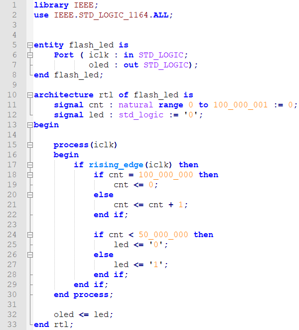
Listing 1 - Module code flash_led
Now create a new module, which should be called brom_reader, its iclk ports with the “in” direction, and odout [7: 0] with the “out” direction (repeat the steps from Fig. 8 to Fig. 12).
If everything is done correctly, then the brom_reader module should appear in the project tree (Fig. 14).
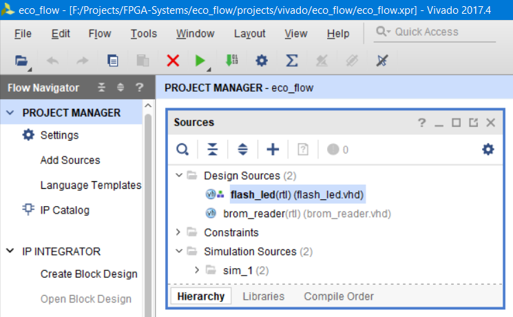
Figure 14 - Module brom_reader in the project tree
Replace the contents of the module with the following text (Listing 2 (text version of Listing 2, see Appendix B)). Here you will need a few comments:
- Line 13: type alias is created for std_logic_vector. Those who work with VHDL often use the data type "std_logic_vector ()". In order not to write these long names each time, you can declare an alias and then use it throughout the module code.
- Lines 14–20: standard declaration of a two-dimensional array of natural numbers and array initialization (memory is created with numbers).
- Line 22: use of the alias slv to declare a signal
- Lines 23-24: use of the synthesis attribute [11]. Why is he registered here? We have created a rather small two-dimensional array (lines 15-20) - and, most likely, during the synthesis it will be optimized and implemented as distributed memory on the LUT. And since we want to place the array in the block memory (BRAM-Block RAM), we need to explicitly tell the synthesizer about this, which is done with the help of synthesis attributes. Read more about them in the Vivado synthesis manual in [11].
Otherwise, everything should be clear: we created a ROM-memory from which its contents are continuously, sequentially and cyclically read.
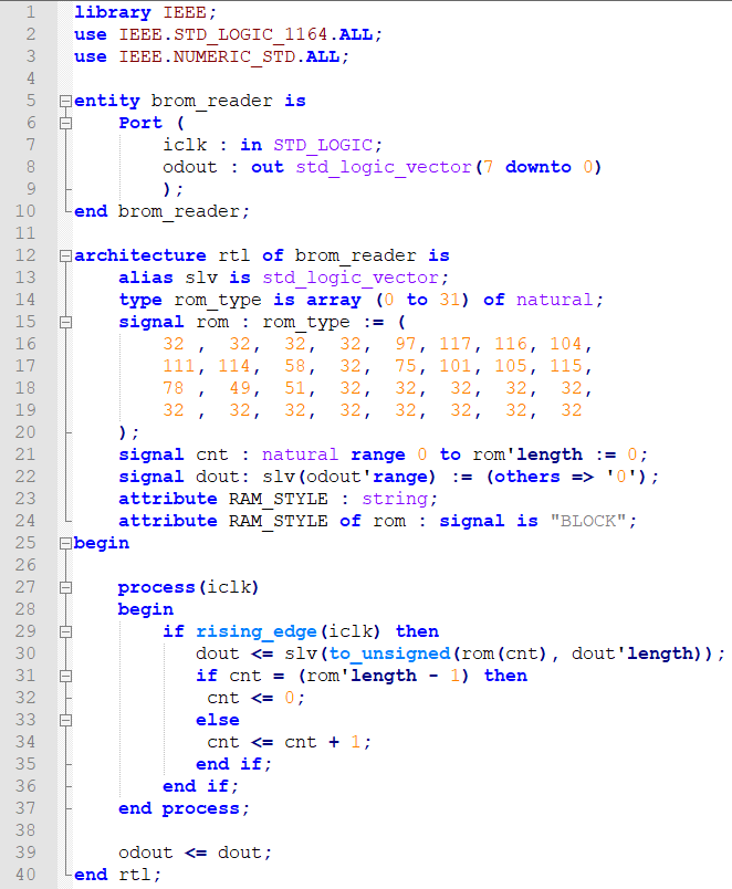
Listing 2 - brom_reader module code
3.3. Creating a MicroBlaze project and working in IP Integrator
Now we will create a project with MicroBlaze. Once again, I would like to draw your attention to the fact that there is a step-by-step guide in Russian on creating projects on the MicroBlaze software processor for beginners [16].
To create a block project, you must create a Block Design. Select Create Block Design, enter the name system and click OK (Fig. 15).
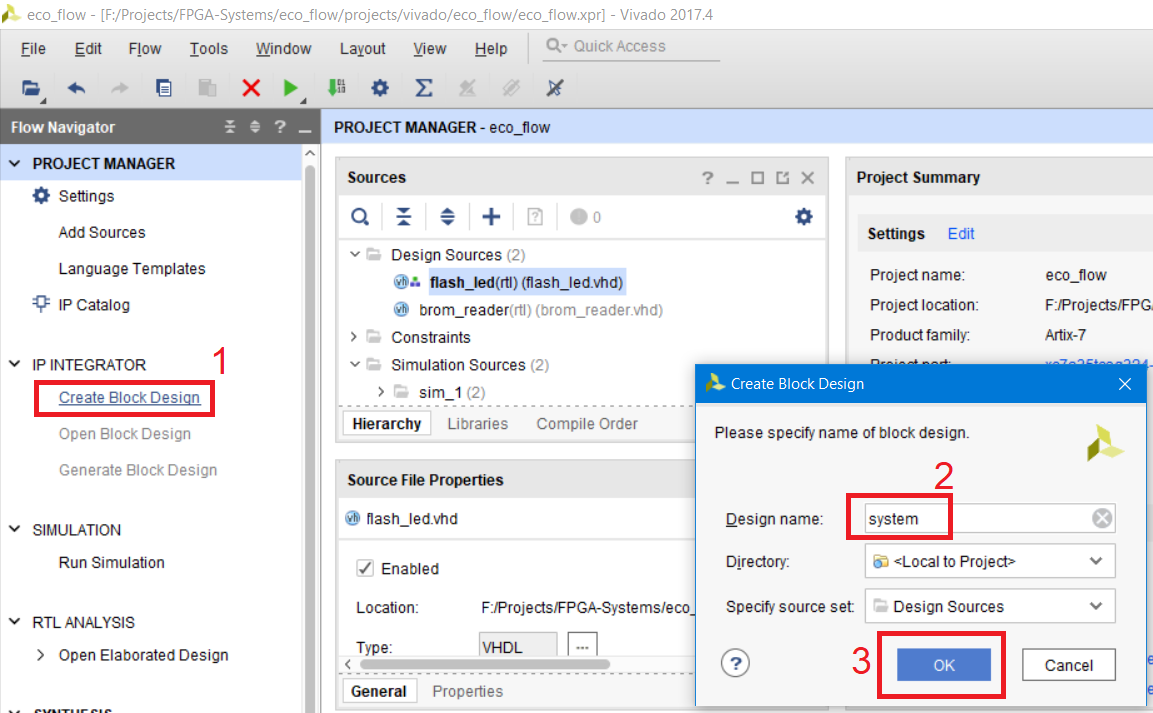
Figure 15 - Creating a new Block Design and setting its name
The Diagram field adds kernels from the Vivado IP directory, or RTL modules written in VHDL / Verilog / SystemVerilog. Find the MicroBlaze module in the IP directory. To do this, click the blue cross and enter “MicroBlaze” in the search field and select it (Fig. 16).
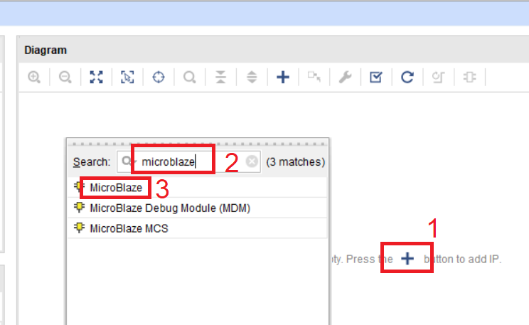
Figure 16 - Adding a MicroBlaze IP core to the Diagram workspace
After adding MicroBlaze to the working field, we will use the express settings of the soft processor. Select Run Block Automation and set the settings in accordance with Fig. 17. Click OK.
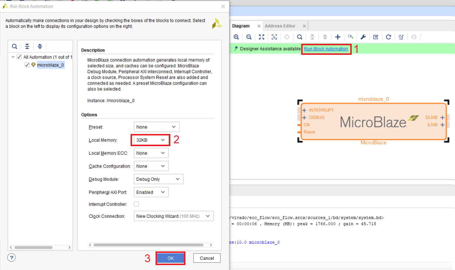
Figure 17 - MicroBlaze Express Setup
After that, several new IP cores will appear on the Diagram work area, including the clock generator and the local processor memory [11, 12]. Click the Regenerate button to optimize the working area (Fig. 18).
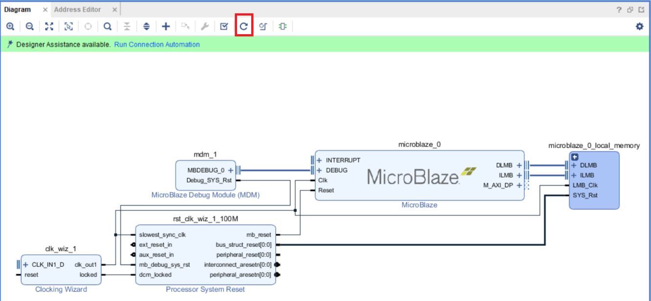
Figure 18 - Basic Power On MicroBlaze
Perform configuration of some modules in accordance with our Arty board. Configure the clock grid generation module clk_wiz_1. To call the module settings, double-click it with the left mouse button. In the settings window, set the value of the input clock frequency of 100 MHz, since it is the generator at 100 MHz that is installed on the board [12]. We also set the type of source as unipolar (Fig. 19). Go to the Output Clocks tab, where we configure the output frequency of the module.

Figure 19 - Setting the input frequency parameters
In the Output Clocks tab, we will set only one frequency, the main frequency of our processor system and other modules. Set it equal to 100 MHz (Fig. 20).
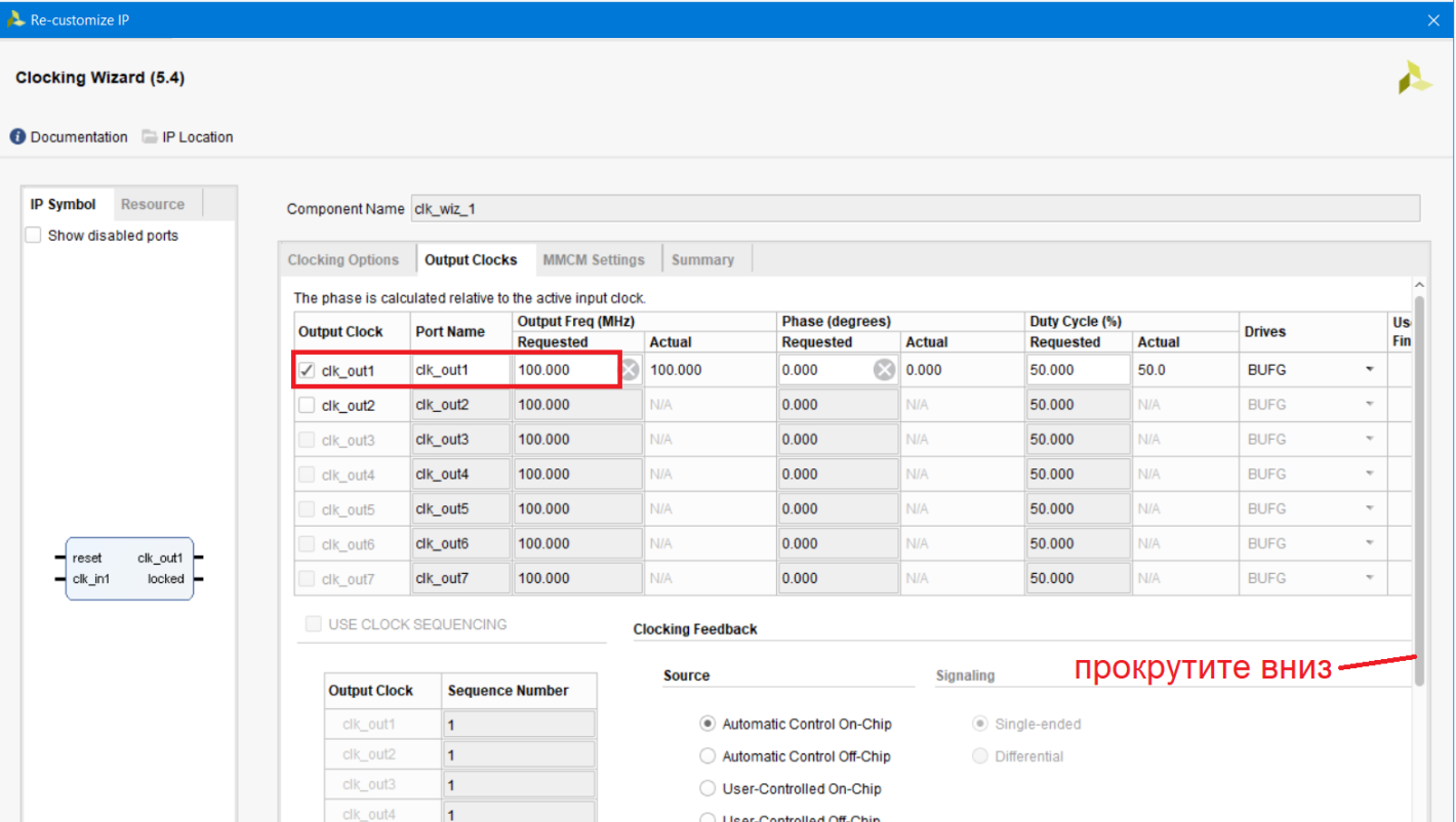
Figure 20 - Setting the parameters of the output frequency
Scroll down to configure additional overhead. We will remove the reset reset signal, which we will not use. Uncheck it (fig. 21). The rest of the settings we do not need, click OK.
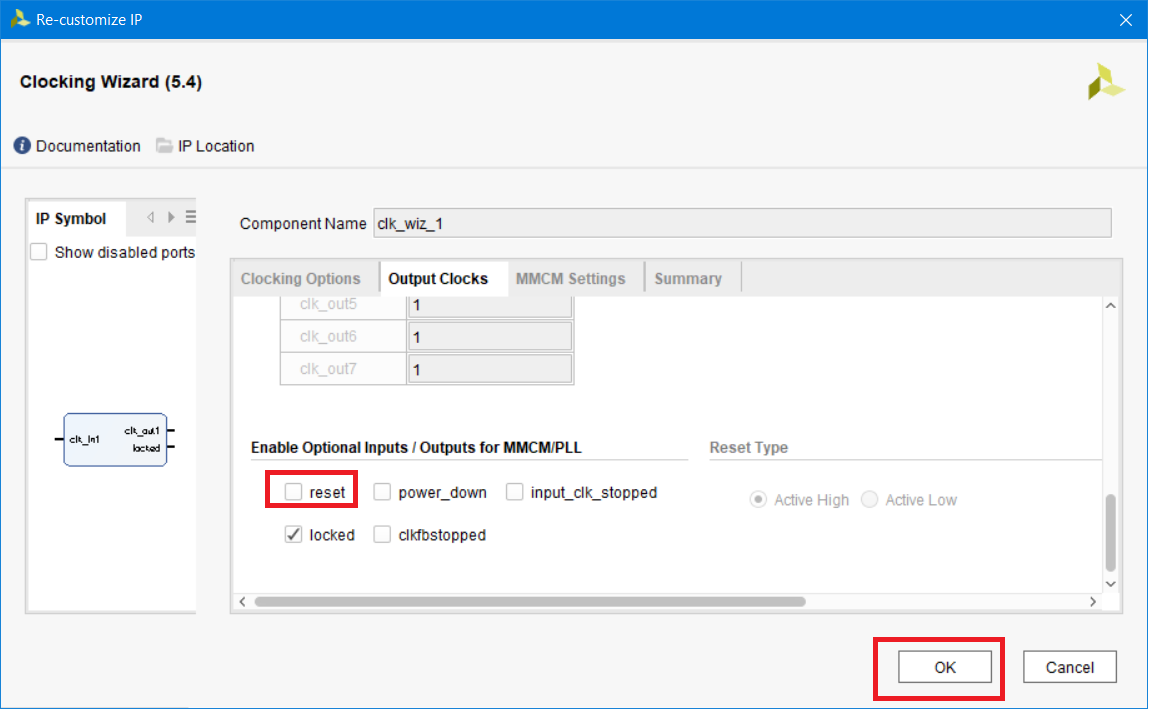
Figure 21 - Configuring service signals
Now we declare the clk_in1 input of the clk_wiz_1 module external, in fact we make from it the input of our Block Design. To do this, click on clk_in1 with the right mouse button and select Make External (Fig. 22).
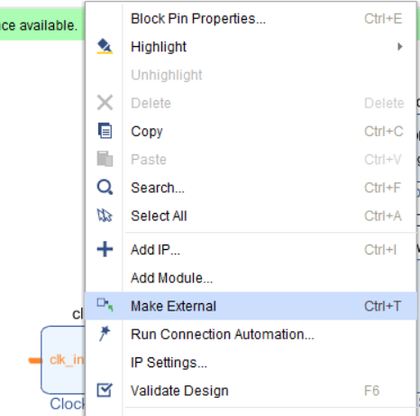
Figure 22 - Making the port clk_in1 external
As you can see port clk_in1_0 appeared (Fig. 23).
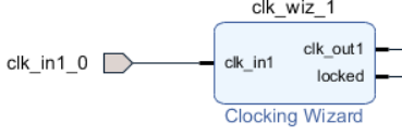
Figure 23 - Input port clk_in1_0
In the reset control module of our processor system, we connect two unused inputs (external reset and additional reset) to the inactive logic level "1". We do this with an IP block called constant. To do this, click the blue cross at the top, then in the search bar enter “const” "and select the module constant.

Figure 24 - Search for the constant IP block in the list of available IPs
Perform the configuration of the xlconstant_0 module by double-clicking on it with the left mouse button. In the line value (Const val) enter 1, in the line width (Const Width) enter 1, press OK (Fig. 25)
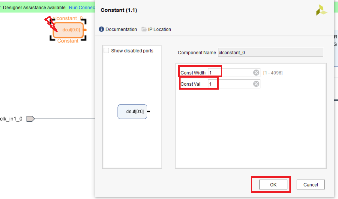
Figure 25 - Configuring the xlconstant_0 module
Let us connect the dout output of the xlconstant_0 module to the ext_reset_in and aux_reset_in inputs of the rst_clk_wiz_1_100M module. Just connect these ports with the mouse (Fig. 26).

Figure 26 - Connecting unused ports to a constant
Add the UART module by finding it in the catalog of available IP cores (Fig. 27).
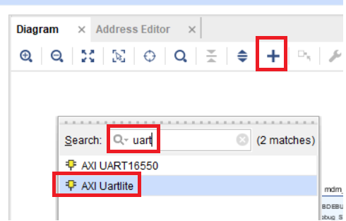
Figure 27 - Search for a UART module in the list of available IP blocks
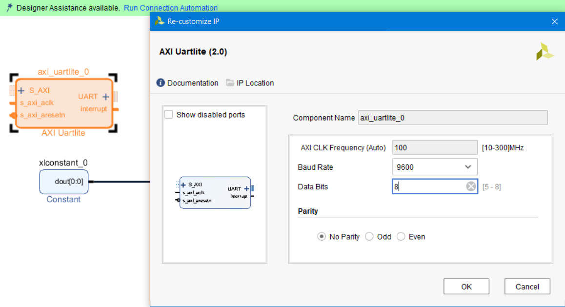
Perform the configuration of the axi_uartlite_0 module, setting the transmission settings in accordance with Fig. 28. Then click OK.
28 – axi_uartlite_0
axi_uartlite_0 . . Run Connection Automation (AXI UART AXI MicroBlaze) . 29.

29 – axi_uartlite_0
UART Vivado IP Integrator. 2 . 29 , rx tx axi_uartlite_0 . , . , , , HDL , , (rx tx).
Regenerate Layout. Block Design , . 30. , . , , , .
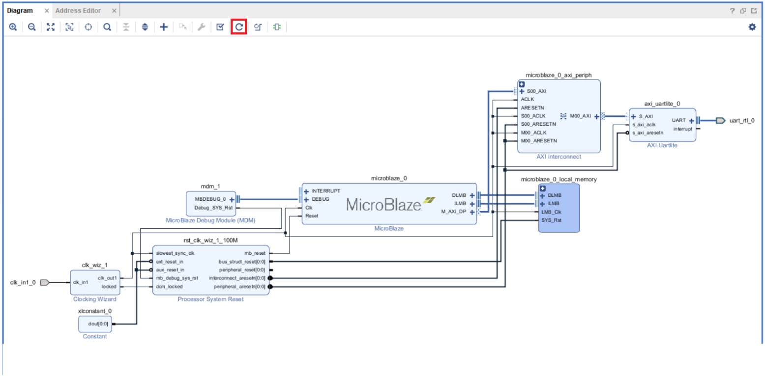
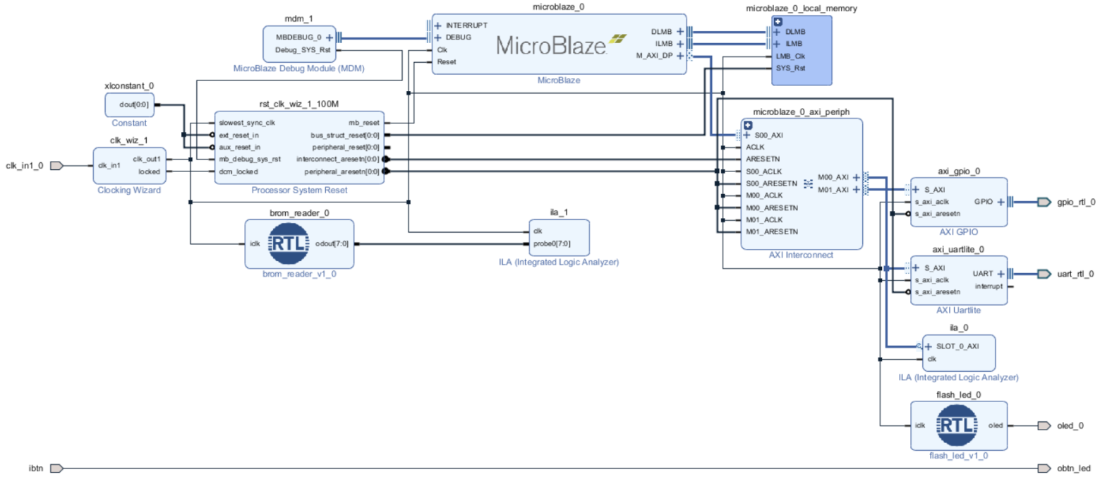
Figure 30 - The intermediate stage of assembly of the processor system.
Let's add one more module to the AXI bus. This will be a GPIO module, the output of which we will connect to the LED. Find the AXI GPIO module in the list of available IP blocks and add it to the working area (Fig. 31). Figure 31 - AXI GPIO module in the list of available IPs

Configure the module in accordance with Fig. 32 (we will use only one channel and one output).
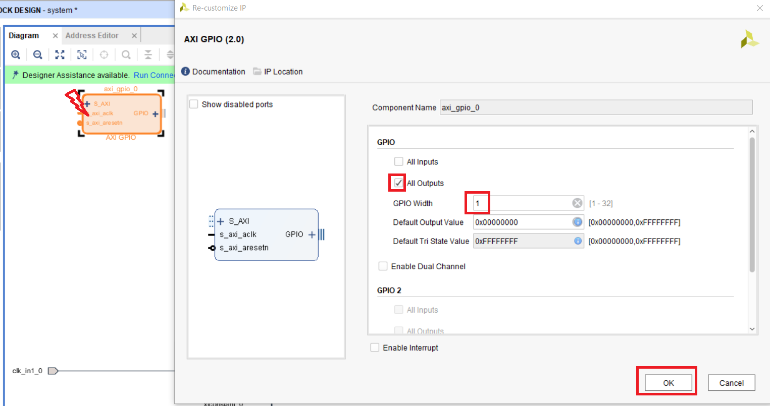
Figure 32 - Settings module axi_gpio_0
Let us connect the axi_gpio_0 module to the processor and make the output external. Click Run Connection Automation and check all the checkboxes (Fig.33).

Figure 33 - Connecting axi_gpio_0 to the processor
Click the Regenerate Layout button and make sure all connections match pic. 34
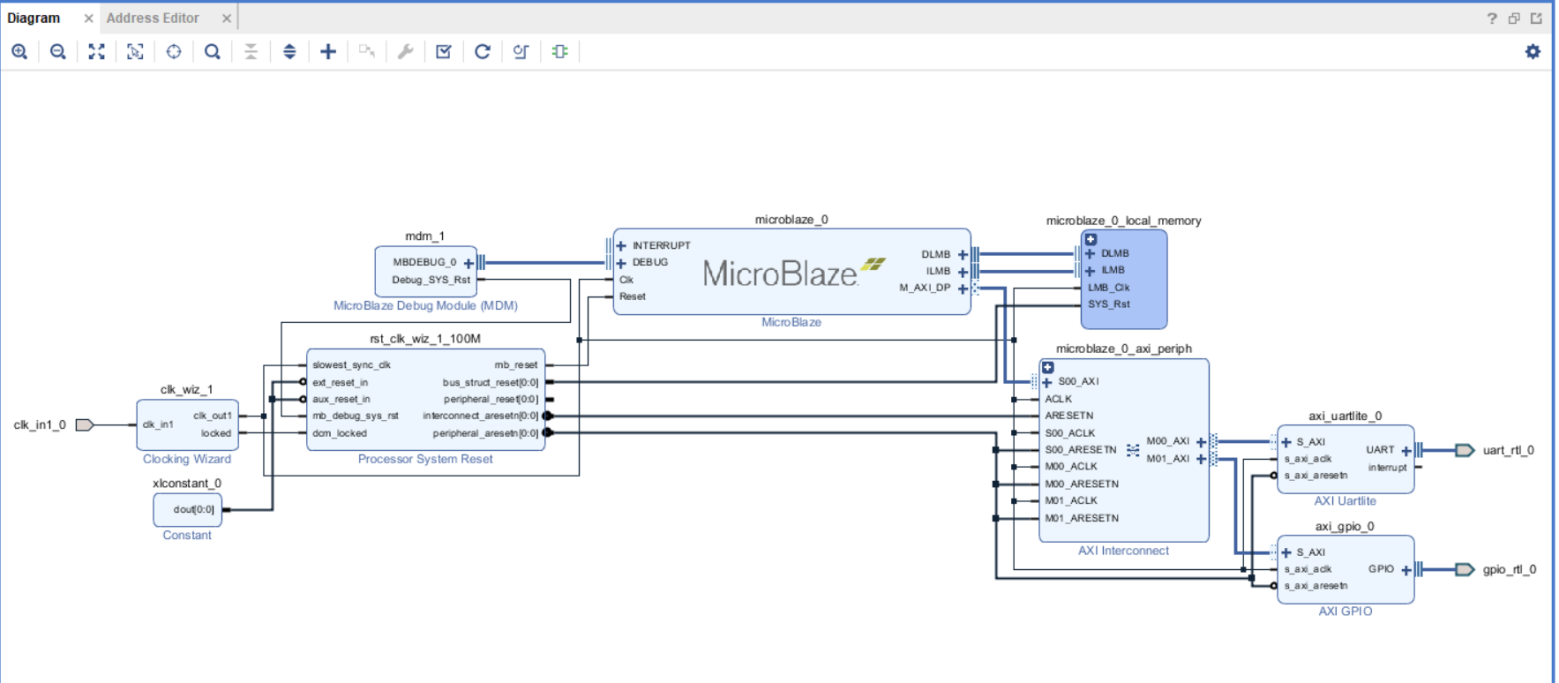
Figure 34 - Assembly of the processor system.
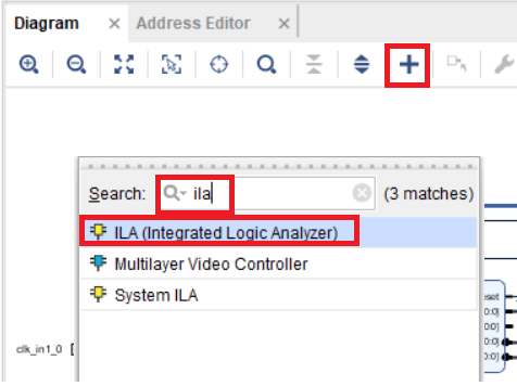
Now add the ILA debug module. Suppose we want to view transactions on the AXI Lite bus for the UART module. Find in the list of available IP module ILA (Integrated Logic Analyzer) fig. 35. Figure 35 - ILA IP block in the list of available
HDL Insertion Flow, HDL . , . Netlist Insertion Flow.
AXI , ILA AXI ( Monitor Type ILA). , SLOT_0_AXI ila_0 AXI, . , axi_uart_0 (. 36). clk Regenerate Layout.

36 – ila_0 AXI axi_uart_0
1024, .
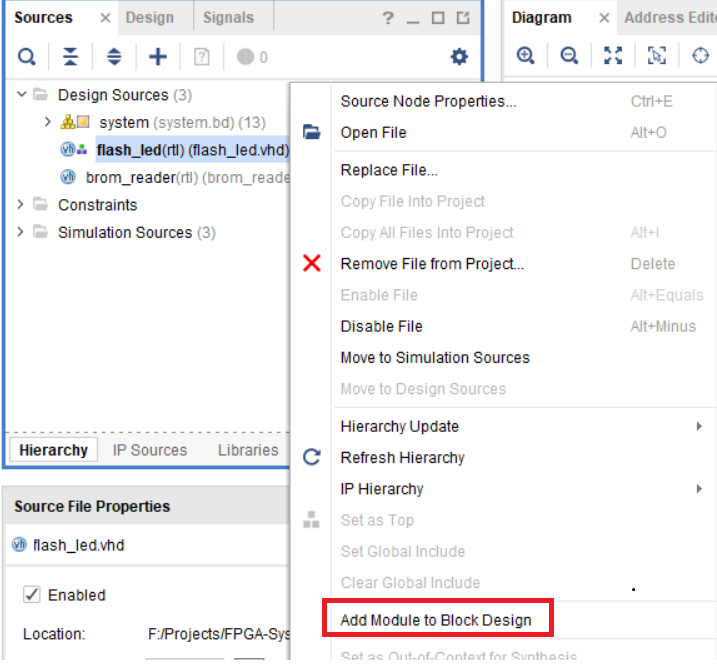
RTL Block Design, flash_led, Add Module to Block Design ( Vivado 2017.1).
37 – flash_led Diagram
iclk flash_led_0 , oled ( , Make Exernal). Regenerate Layout.
, . 38.
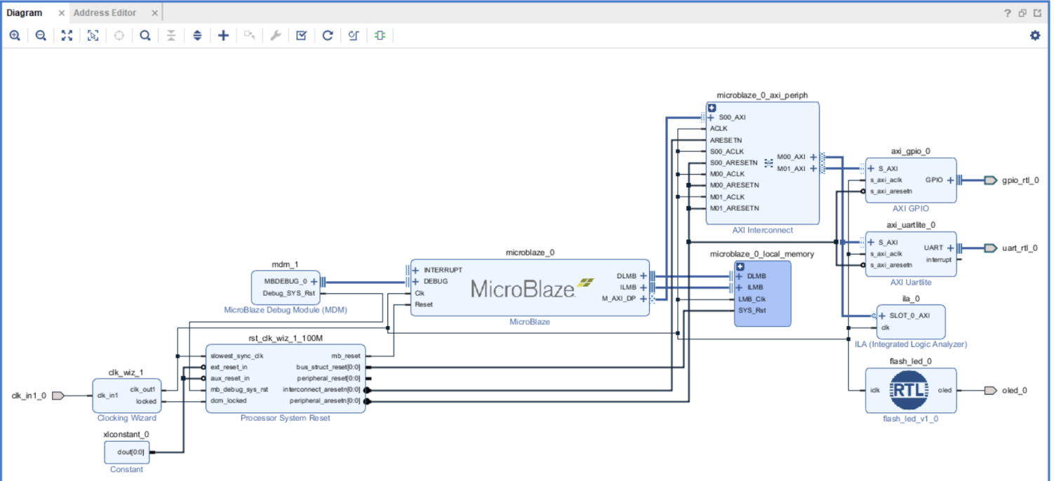
38 – IP Integrator
, brom_reader. iclk , odout[7:0] . Regenerate Layout. , . 39.
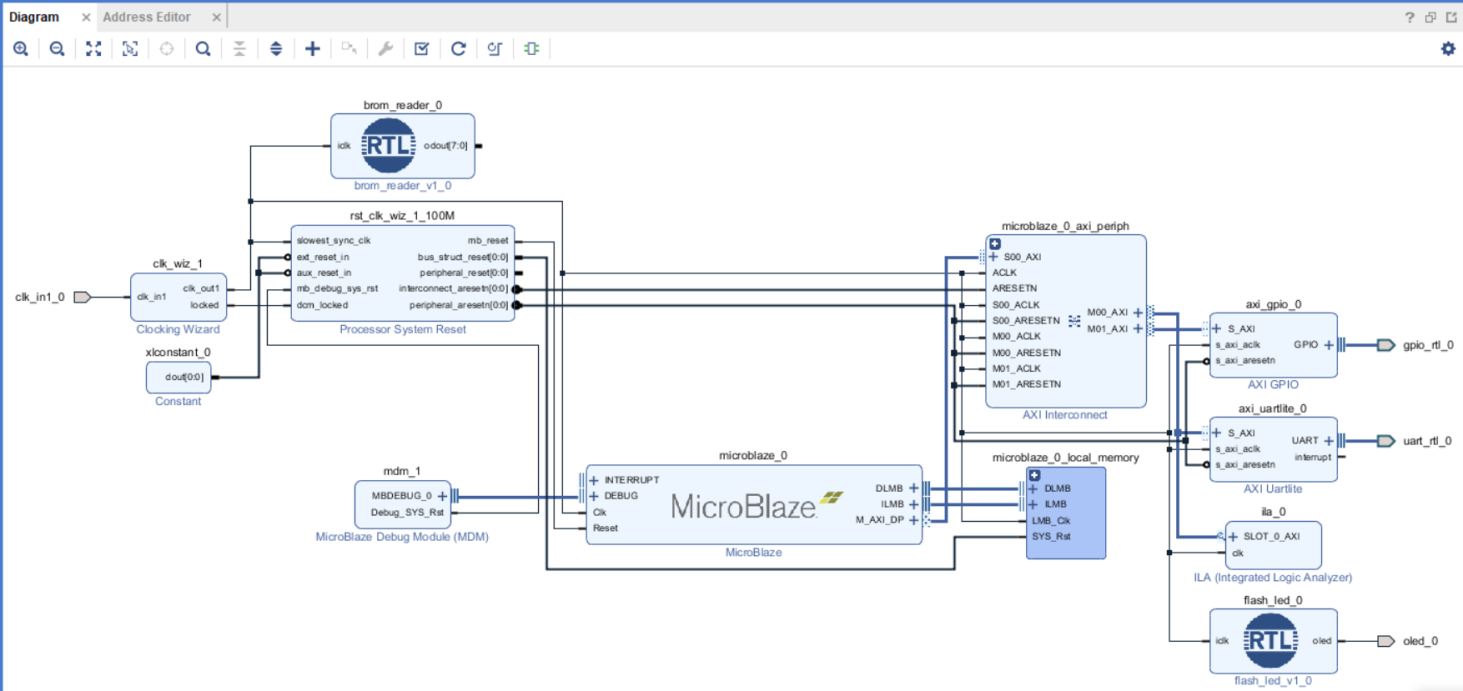
39 – IP Integrator
, ILA odout[7:0] brom_reader_0.
IP ILA (. 35) Diagram. , . Monitor Type Native ( AXI, ). . Probe_Ports(0..7) . 40.
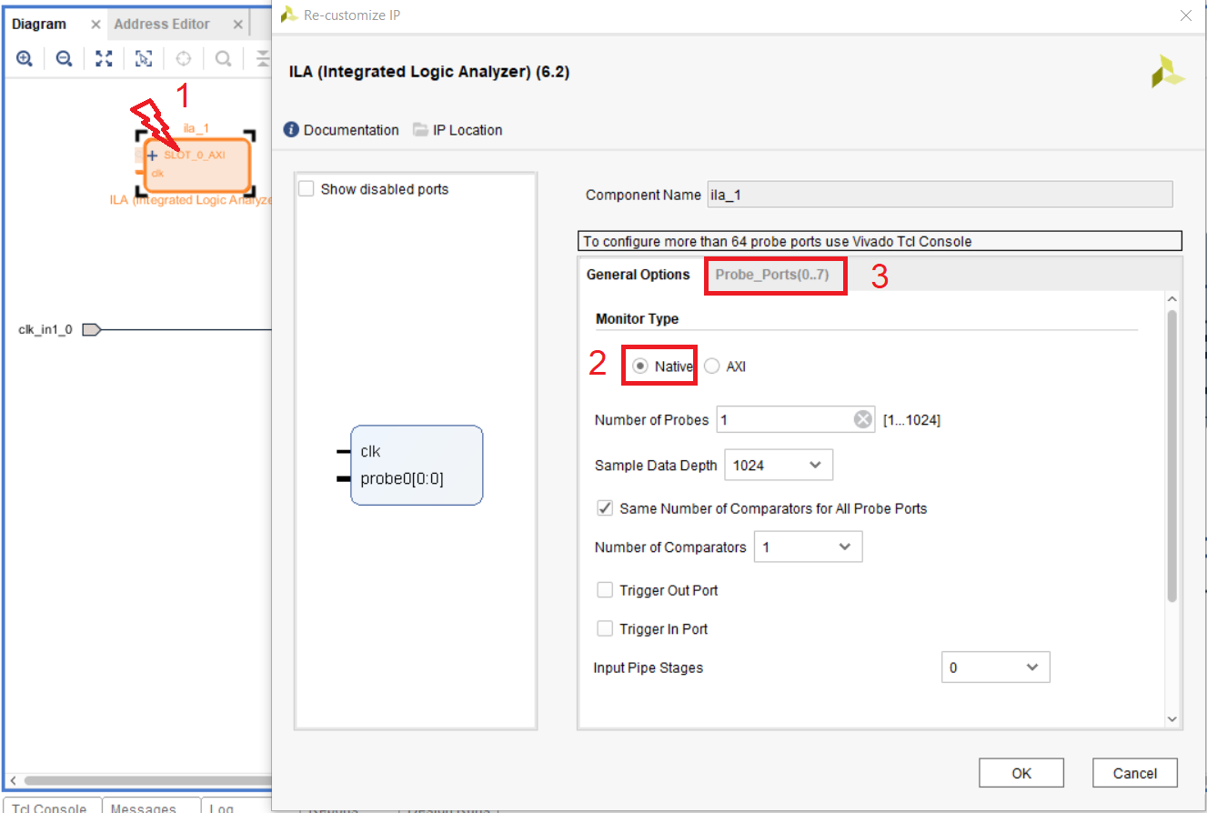
Figure 40 - ILA Setup Set the
probe width. Set the width to 8 (Fig. 41), since it is 8 bits that is the width of the odout [7: 0] output bus of the brom_reader_0 module. Click OK.
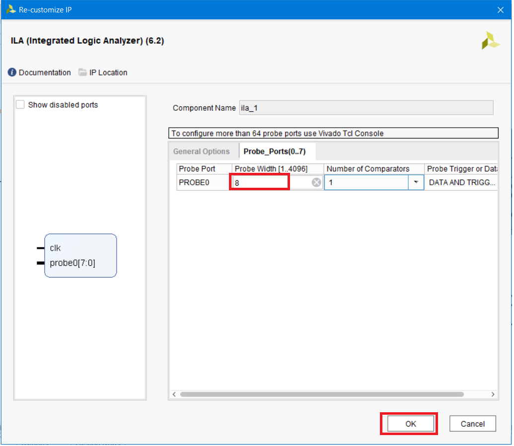
Figure 41 - Setting the width of the ILA probes
Connect the odout [7: 0] output of the brom_reader_0 module to the probe_0 [7: 0] input of the ila_1 module, and connect the clk input of the ila_1 module to the clock circuit of our project. Click the Regenerate Layout button, and if everything is correct, it should turn out as in fig. 42

Figure 42 - Intermediate stage of building a project in IP Integarator
It remains only to add the button and the LED directly connected to it.
Create an input port by clicking on an empty space of our block diagram with the right mouse button and selecting Create Port (Fig. 43).

Figure 43 - Creating a port in IP Integrator
, ibtn, input , . OK (. 44).
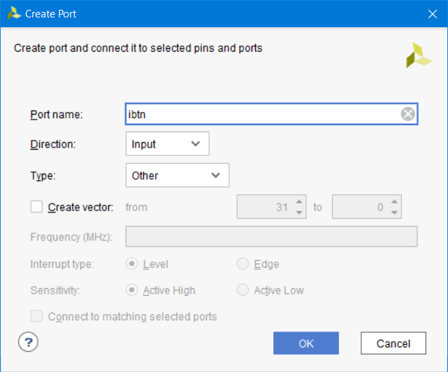
44 – ( ibtn)
Diagram (. 45).

45 – ibtn
obtn_led, output ( . 43-44).
ibtn c obtn_led, Regenerate Layout. . 47.
46 – IP Integrator
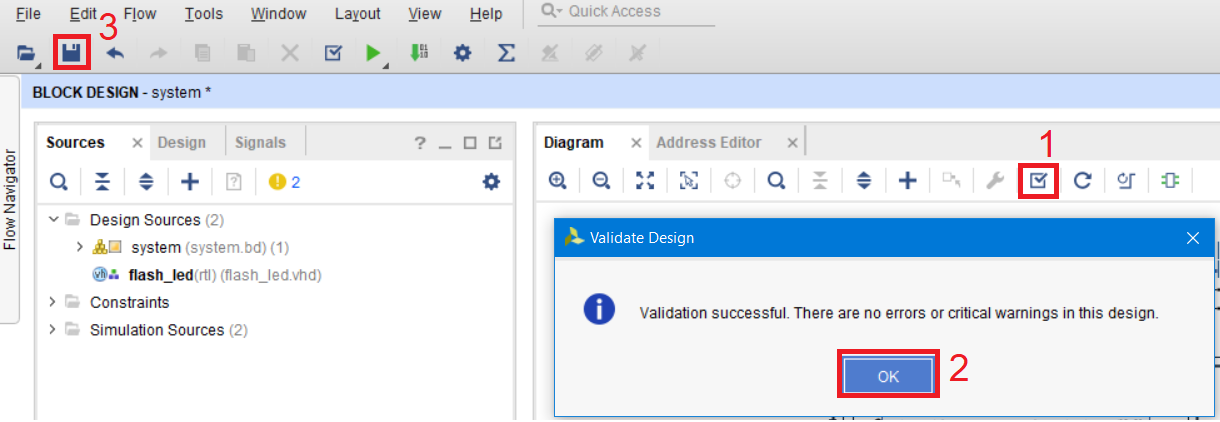
, Block Design, Validate Design. , Vivado . OK Block Design (. 48).
47 – IP Integrator
3.4.
Go to the Sources tab, right click on the system and select the Create HDL Wrapper option (create an HDL wrapper for our Block Design) pic. 48
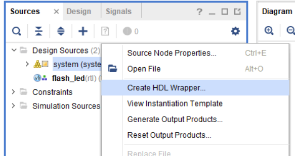
Figure 48 - Creating a project wrapper
After that, Vivado will offer to manually update the HDL wrapper when you make changes to Block Design, or to do it automatically. We leave the automatic update and click OK (Fig. 49).
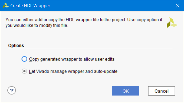
Figure 49 - HDL Wrap Upgrade Options
Now we point out that the system_wrapper module is a top module. Right-click on system_wrapper and select Set as Top (fig. 50).
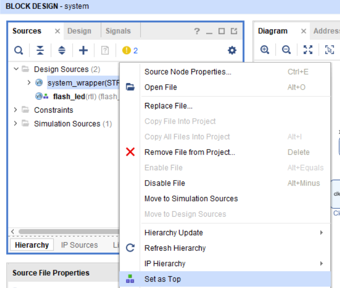
Figure 50 - Making the system_wrapper module a top module
Now let's perform the synthesis of the system_wrapper module by clicking on the Run Synthesis button (Fig. 51).
Note: to connect the debugging blocks, we actually used HDL Insertion Flow [4], that is, we actually inserted our ILA blocks into the code and connected circuits to them. It makes no difference how you create and connect circuits for debugging: via HDL or Netlist. In the end, ECO works with synthesized or implemented netlist that is stored in Design Checkpoint.
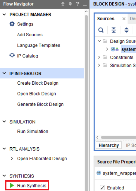
Figure 51 - Starting the synthesis of the project
After clicking on the Run Synthesis button, click OK and wait until the synthesis is complete.
After the end of the synthesis, a window will be displayed in which you will be asked to start the implementation, open the results of the synthesis or view the reports. Open the results of the synthesis (Fig. 52).

Figure 52 - Opening the results of the synthesis
Now we connect the legs in our project. This is done using Pin Planer. To open it, click Window → I / O Ports (fig. 54).
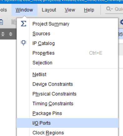
Figure 53 - Opening the window for pin assignment
Using the Reference Manual [12] for Arty, assign the legs (Fig. 54).
BE CAREFUL!!! I specifically confused the legs for the UART rx and tx module!
Assign the legs in accordance with Fig. 54.
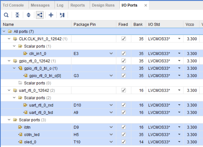
Figure 54 - Assignment of project legs (rx and tx UART are confused specially)
Click the save button, after which Vivado will indicate that you did not create the design constraints file, and will offer to create it. Enter the file name constr and click OK (Fig. 55).
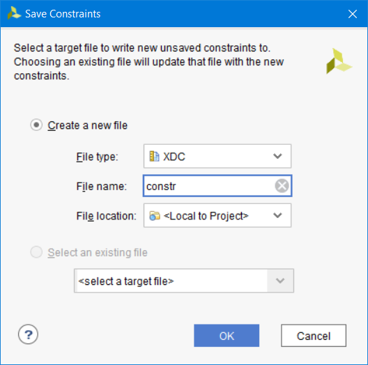
Figure 55 - Creating a design constraint file
. Generate Bistream, OK (. 56).

56 – Generate Bitstream
Bitstream . Cancel (. 57)
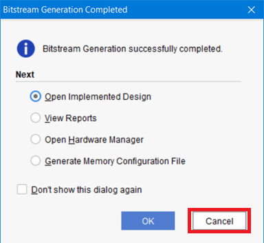
57 –
3.5. MicroBlaze
MicroBlaze. Xilinx Software Development Kit (SDK). SDK (IP , AXI) SDK. File → Export → Export Hardware (. 58).
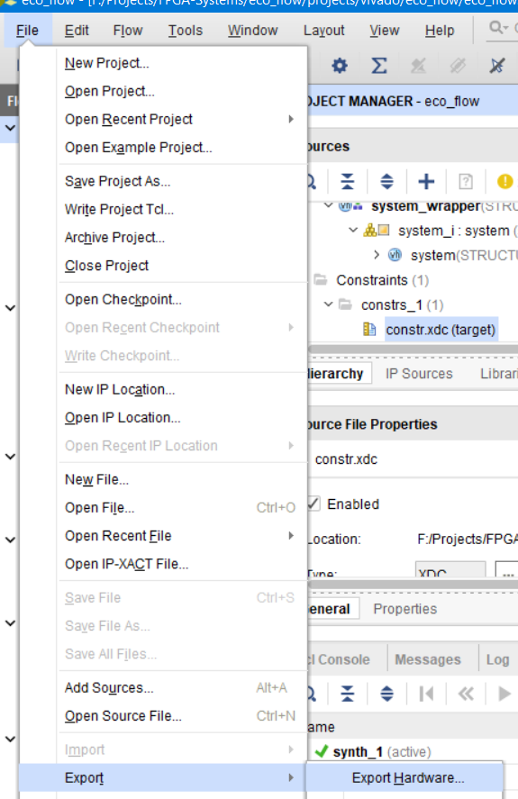
58 – SDK
In the window that appears, do not check the Include Bitstream box. Leave the default settings and click OK (Fig. 59).
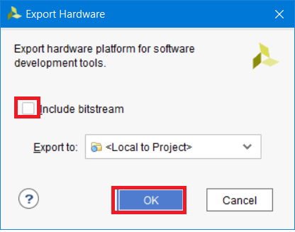
Figure 59 - Export Parameters Window
Now run the SDK. To do this, select File → Launch SDK
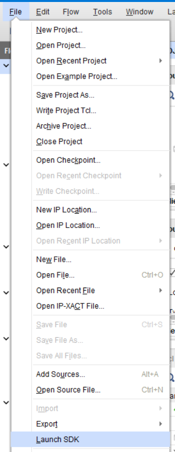
Figure 60 - Launch the SDK
Wait until the end of the SDK service operations. After they are finished, we can start creating a new project. Choose File → New → Application Project.
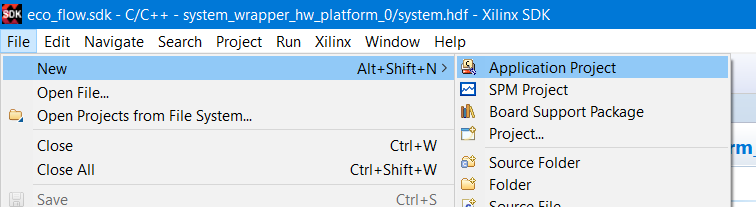
Figure 61 - Creating a new project in the SDK
Enter the name of the new MB_run project, click Next (fig. 62)
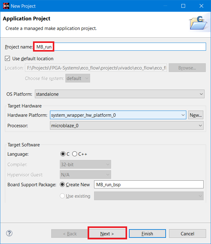
Figure 62 - Setting up a new project
In the ready-made templates window, select the creation of the Hello World application and click Finish (fig. 63)
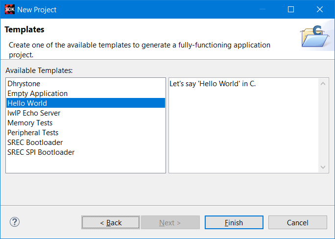
Figure 63 - Selecting a template for the project being created
Open the file helloworld.c (the location of which is shown in Figure 64) and replace its contents with the program code shown in Listing 3, and save the result.
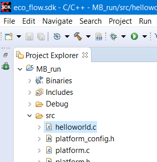
Figure 64 - Location of the helloworld.c file Listing 3 - Replaced contents of the helloworld.c file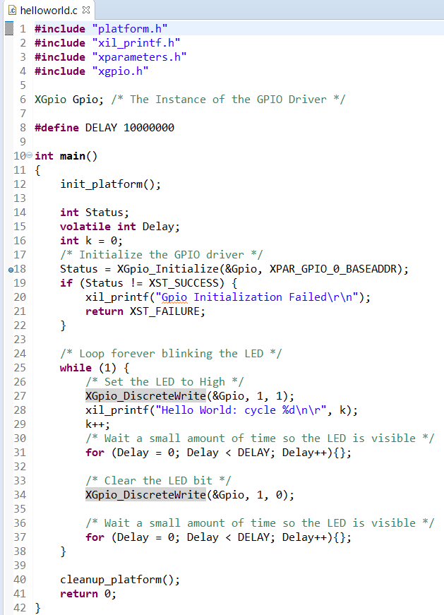
The program sends “Hello World: cycle” approximately once every 2 seconds and blinks with the LED LD1 (red component) also approximately once every 2 seconds.
3.6. Running the program and debugging
After writing the code and assembling the processor system, you need to make sure that:
- LD4 LED is lit by pressing the BTN0 button
- The processor works and sends “Hello World: cycle” to the console, however, we don’t see the words in the console, because we made the wrong connection rx and tx. An additional signaling device of the processor is the flashing LED LD1.
- AXI-Lite transactions from the processor to the UART are executed.
- The block memory is read and gives the correct values.
First we connect Arty to the computer. Perform the setting of the terminal in which the UART messages should be displayed. This can be done using standard SDK tools. The SDK has a terminal located below (Fig. 65).
If there is no terminal, then it can be found in Window → Show View → Others → Xilinx → SDK Terminal (Fig. 65).
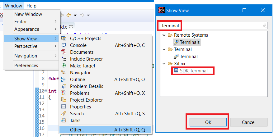
Figure 65 - Opening the embedded terminal in the SDK
Set the terminal settings, in accordance with Fig. 66. COM port number may vary.

Figure 66 - Configuring the terminal's SDK
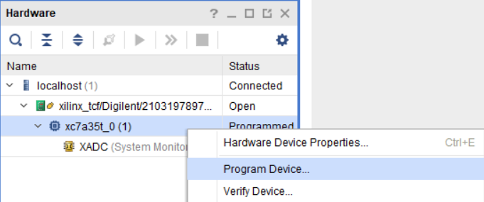
Now let's go to Vivado and execute FPGA programming.
Click Open Hardware Manager and go to programming and debugging mode. Select Open Target and click Auto Connect Auto Connect (Fig. 67)

Figure 67 - Opening the Hardware Manager and connecting to the FPGA
(. 68)
68 –
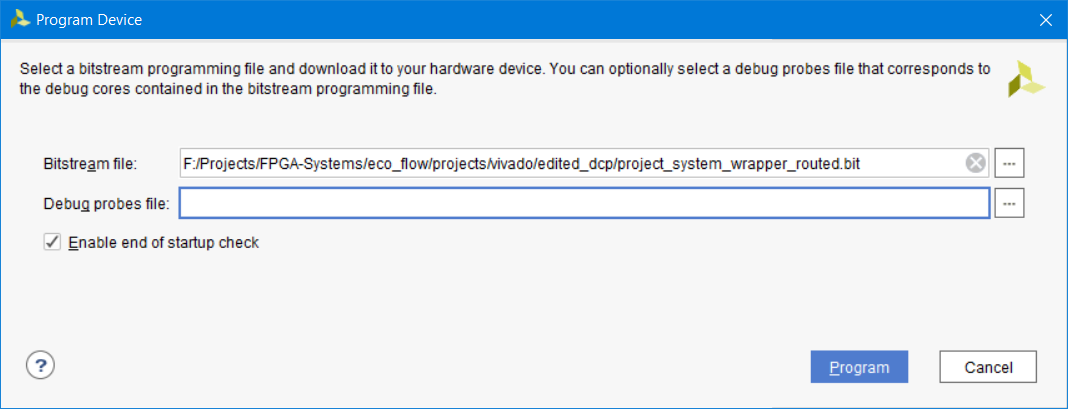
, .bit .ltx (.69) Program.

69 –
, LD4 , BTN0 LD4.
UART LD1.
SDK, MB_run, Run As → Launch on Hardware (System Debugger), . 70. , .
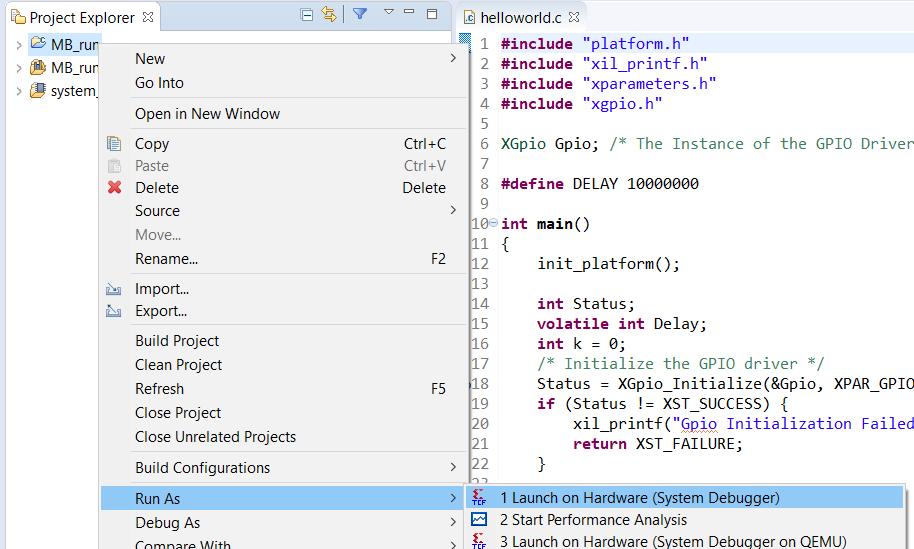
70 –
, , LD1 , SDK Terminal , rx tx .
, , UART - .
Vivado. , , ILA: AXI UART, . ILA (. 71).

71 – ILA
, , , , . , , UART - . «», , , , ILA.
hw_ila_1 .
Trigger Setup , . , . 72. OK.
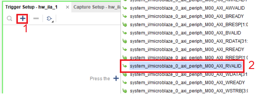
72 – ILA
: AXI-Lite, . , . , , [14].
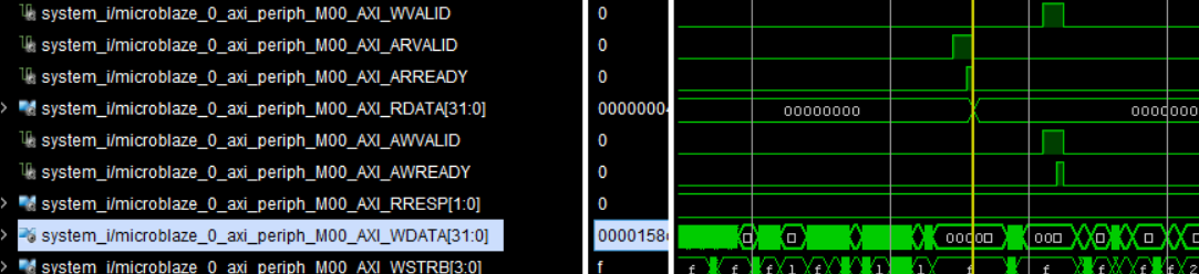
. RVALID «1», , , «1». , . 73. .

73 – ILA
, , , . . 74
74 – AXI-Lite
Change the displayed bus status to ASCII. To do this, right-click on the bus, then select Radix, then ASCII (Fig. 76).

Figure 75 - The choice of data representation on the bus * WDATA [31: 0]
After that we will see on the bus a part of our message that the processor sends out. This partially confirms that the transaction is correct (Fig. 76).

Figure 76 - ASCII representation of data on the bus * WDATA [31: 0]
Try repeating the actions from fig.71 to fig. 76 for hw_ila_2, which is connected to the output of the block memory reader module. Install the trigger is not required. If everything is done correctly, the picture should be similar to fig. 77.
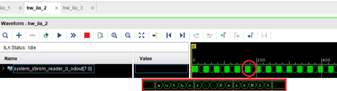
Figure 77 - Data read from block memory
This completes the test project build, and we can start editing our netlist and working in ECO mode.
4. ECO
:
- BTN0
- UART , ( rx tx)
- ( ASCII:”author: KeisN13”).
, ECO, Design Checkpoint (DCP). DCP, (post route).
Vivado DCP, DCP «» DCP .
edited_dcp. (. 78)
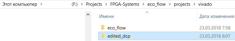
78 – DCP
DCP , «_/_.runs/_/___routed.dcp» (. 79) edited_dcp.
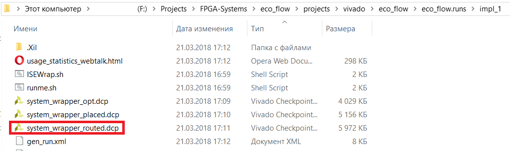
79 – DCP
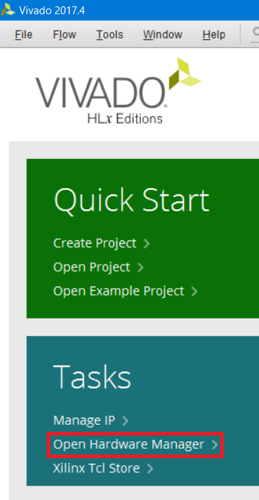
Go to Vivado and perform the opening of the DCP. To do this, click File → Open Checkpoint (Fig. 80)
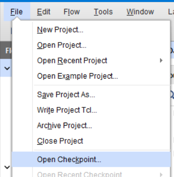
Figure 80 - Opening DCP
Select the location of the copied DCP file in the edited_dcp folder and click OK.
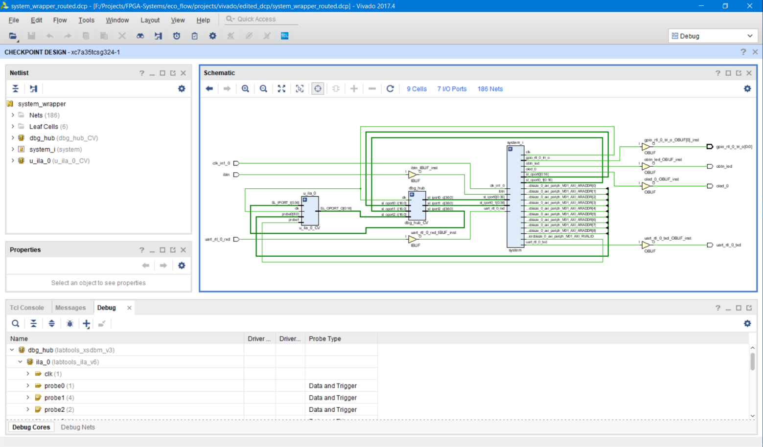
After opening the DCP, by default, the view (perspective) Default will be opened, or the one that you used the last time, if you opened the DCP (Fig. 81). Figure 81 - Debug Open DCP Perspective
There are several modes of operation with DCP, but today we are interested in ECO Flow. To switch to ECO mode, you must change the view. To do this, select ECO in the upper right corner of the drop-down list (Fig. 82).
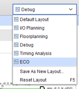
Figure 82 - Transition to ECO mode
, ECO (. 83). , .

83 – ECO
5. ECO:
ECO , . 84. DCP. DCP , / Tcl-. , , , . , (, .bit) (.ltx). « », , . – DCP .
84 – ECO
. [3] Vivado ECO Flow.
ECO , , .
ECO Navigator, . ECO Navigator .
Edit (. 85): ,

85 – Edit
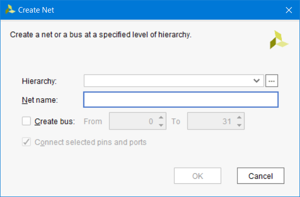
Create Net: , . , . . pin port, , Connect selected pins and ports (. 86).
86 – Create Net
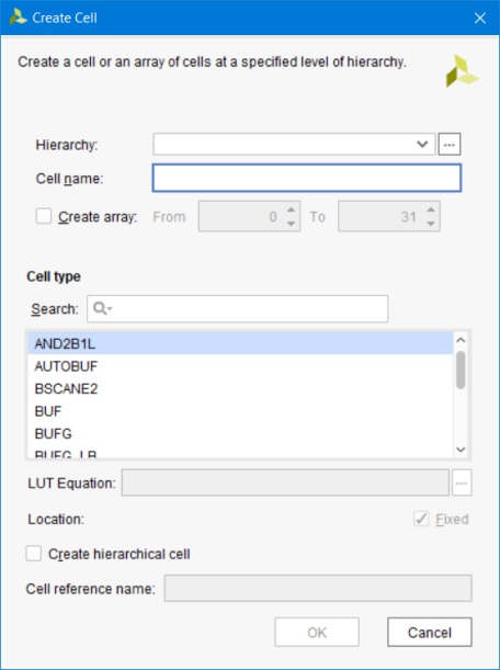
Create Cell: , . . , , black box. LUT, , (. 87).
87 – Create Cell
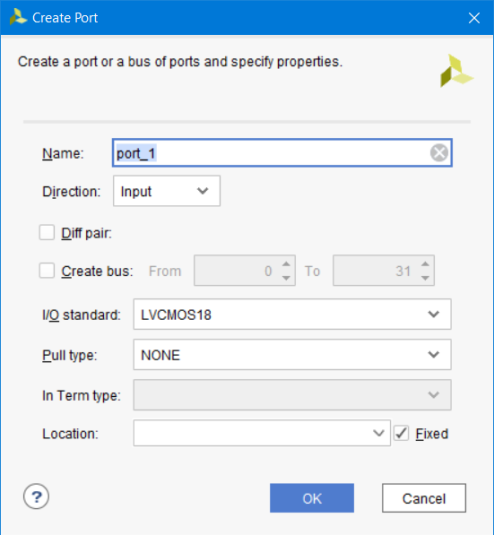
Create Port: . : , , .. (. 88).
88 – Create Port
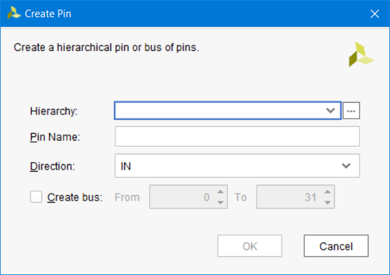
Create pin: . ( cell) . create_port. , (. 89).
89 – Create Pin
Connect Net: . . , .
Disconnect Net: , . , cell, , .
Replace Debug Probes: , ILA / VIO (Virtual Input Output), , .
Place Cell: cell .
Unplace Cell: cell .
Run
Run , .
Check ECO: Runs error checking (DRC - Design Rule Check)
Note: Vivado allows you to make many changes to a netlist using ECO mode commands. However, the logical changes made to the project can lead to impracticable physical implementation. Running Check ECO should be done before you decide to implement the project to eliminate errors in the early stages of the ECO Flow route.
Optimize Logical Design: in some cases it is recommended to perform netlist optimization using the opt_design command and its corresponding options [9]. Optimize Logical Design allows you to call a dialog box that allows you to enter the appropriate Tcl arguments of the opt_design command, which are specified in the options string.
Place Design: Performs an incremental (i.e. based on the previous netlist) component layout of the current netlist. The Incremental Placement Summary report, which is displayed in the console at the end of the place_design command, allows viewing statistics on the reuse of the previous placement, which was in the original DCP before making changes. Clicking Place Design brings up a window in which the appropriate options for the place_design [9] command can be set. For more information on incremental implementation, see [3] in the Incremental Compile section.
Optimize Physical Design:in some cases, it may be necessary to perform a physical optimization (phys_opt_design command [9]). The dialog box invoked by clicking on Optimize Physical Design allows you to enter the appropriate options for the phys_opt_design command.
Route Design: brings up a dialog box that allows, depending on the choice, to perform an incremental trace of the changes made to the netlist, the trace of the selected pins or chains. In case the percentage of reused eroded chains is less than 75%, then an ordinary netlist trace will be fired.
For more information on incremental implementation, see [3] in the Incremental Compile section.
Report Section
In this section, it is possible to generate the necessary reports for the modified netlist, including a report of the resources used, temporal characteristics, the intersection of clock domains, etc.
Program Section The
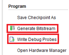
tools of this section allow you to save the changes you made to the new DCP, create the FPGA firmware file, create a new sheet of circuits being debugged via the ILA, in case the ILA has been modified, program the FPGA and debug using standard V Manager Hardware Manager.
Scratch
, , , . Con , PnR .
Scratch (. 90). , , . , [3] Vivado ECO Flow → Scratch Pad → Scratch Pad Pop-up Menu.

90 – Scratch
6.
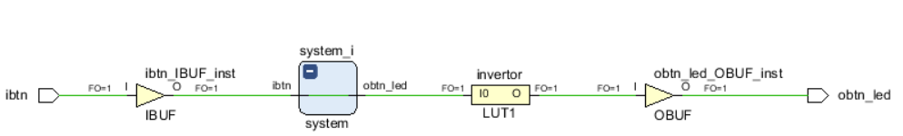
. , , . , LD0 , BTN0 . , , .
6.1.
, ibtn, , F4. , , .

91 –
, ibtn. ibtn LD1 ( obtn_led). ibtn, Expand Cone To Flops or I/Os. Regenerate Layout (. 92)

92 – ,
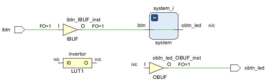
«» (. 93).

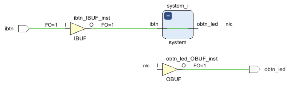
93 – «» ibtn obtn_led
, , , . system_i . obtn_led system_i I obtn_led_OBUF_inst, Edit Disconnect Net.

94 –
Regenerate Layout , (. 95)
95 –
Scratch Pad, .
. Edit Create Cell, invertor, INV OK (. 96)
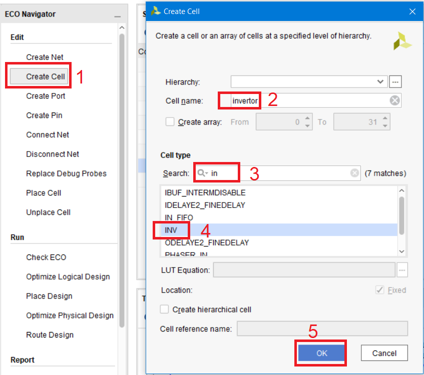
96 –
INV (. 97)
97 –
, LUT. , LUT , , , Cell Properties, Truth Table Edit LUT Equation… (. 98).
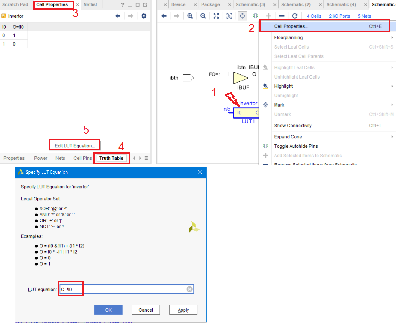
98 – LUT
. , Scratch Pad I0 invertor obtn_led system_i.
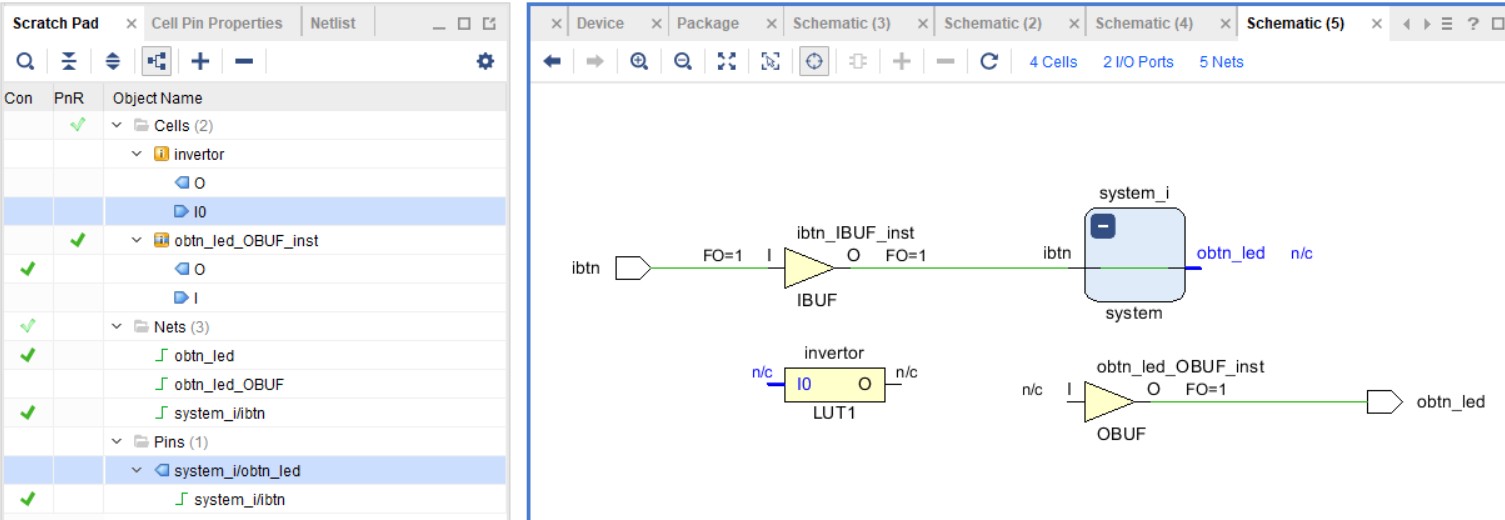
99 –
. Edit Create Net. btn_led, (. 100)
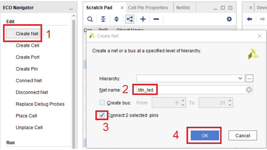
100 –
. Regenerate Layout (. 101)

101 –
O invertor I obtn_led_OBUF_inst. -, . btn_led_o. . 102
102 –
DCP , (. 103).
103 – ECO
Due to the fact that we did not perform the placement and tracing, a series of errors will appear that speak of this.
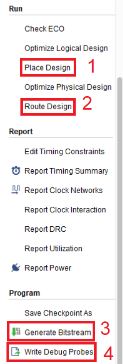
Now we will try to generate a bit firmware file, and see if it worked out to make changes correctly. To do this, you must consistently perform the steps from the section Run, not all of course and without any options. Everything remains by default (fig. 104).
Click Place Design and without entering any options click OK. After waiting for the completion of operations, click Route Design and select Incremental Route in the window that appears, click OK.
After that, we generate a bit file by clicking on Generate Bitstream. Make sure that the edited_dcp folder is in the file path field. After that, open the Hardware Manager for the firmware of our FPGA.
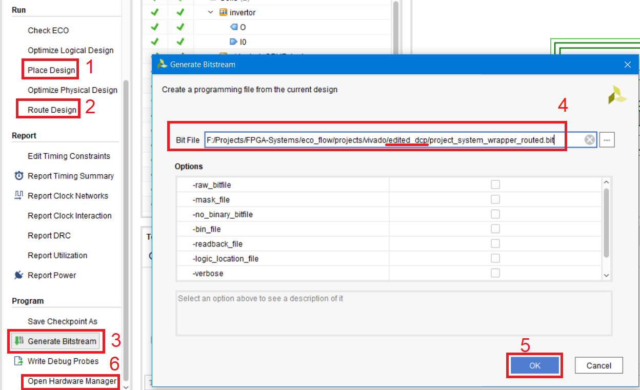
Figure 104 - Sequence of actions for obtaining the firmware file .bit
, Vivado. , Vivado Hardware Manager (. 105). , .bit ILA .ltx
105 – Hardware Manager Vivado
, .67-69 . , , edited_dcp (. 106).
106 –
, LD0 , BTN0 .
6.2. /
ECO . brom_reader, , , . BROM INIT, .
Netlist brom_reader (.107).
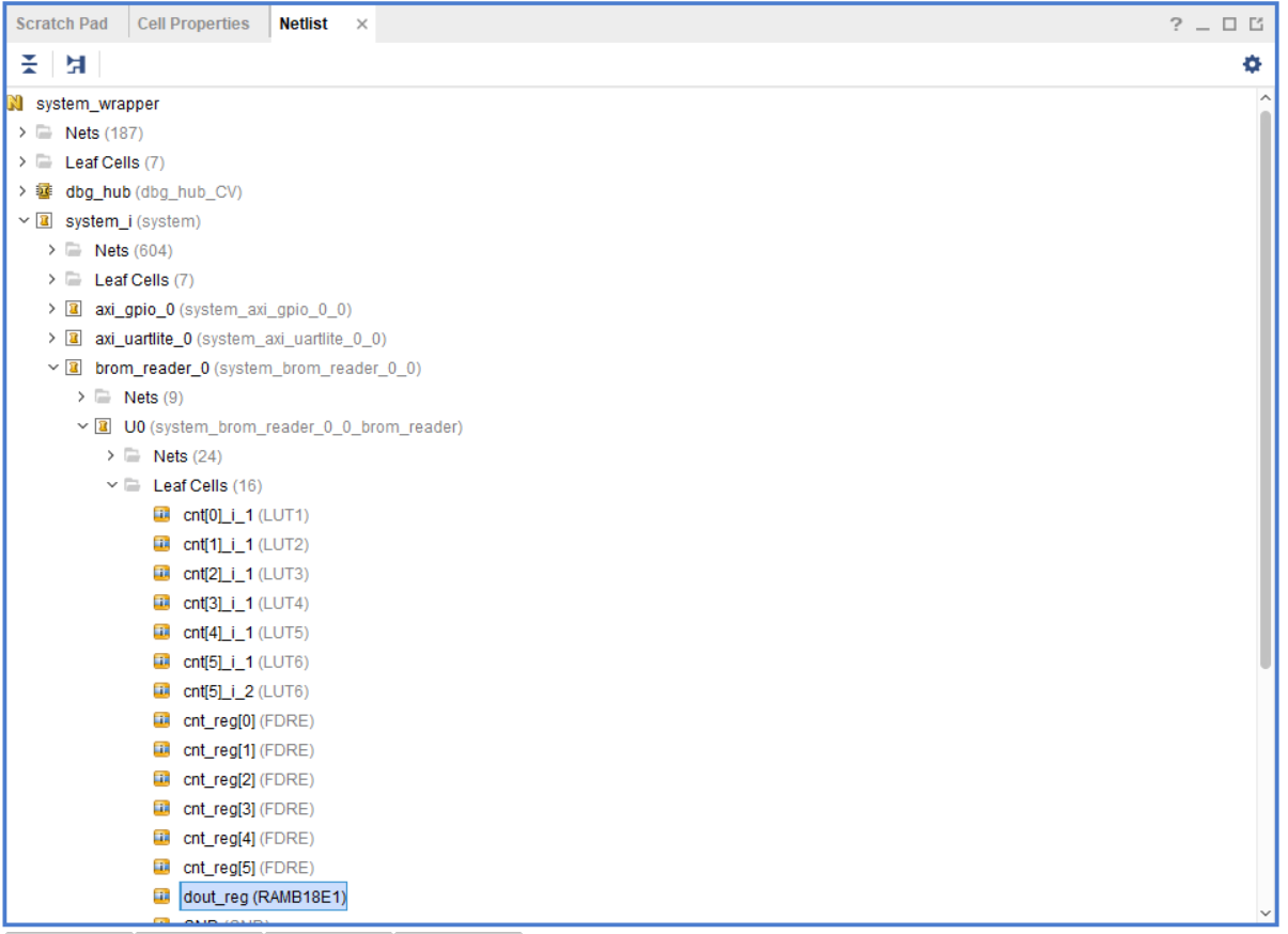
107 – brom_reader
, , Cell Properties (. 108). Properties INIT.
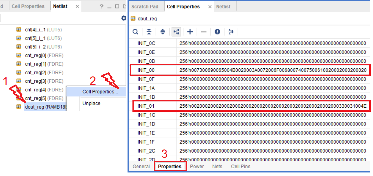
Figure 108 - INIT properties of the selected block memory
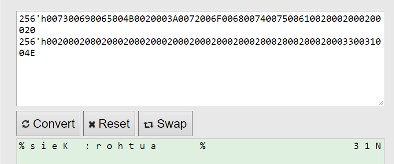
As you can see, the initialization values of the block memory are stored in the INIT properties. Among the many of these properties, we are interested only in INIT_00 and INIT_01. If you copy the contents of these two properties of the HEX to ASCII converter [15], you get the inscription, which we saw in fig. 77, but written in reverse order (Fig. 109) Figure 109 - The content of the INIT properties in ASCII format
You can change the property of a component by clicking on the pencil icon and entering new values or using the Tcl console and the set_ptoperty command.
Replace the property values according to Fig. 110 and save the result:
INIT_00: 256'h0061006700700066002E00770077007700200020002000200020002000200020
INIT_01: 256'h0020002000200020002000750072002E0073006D00650074007300790073002D
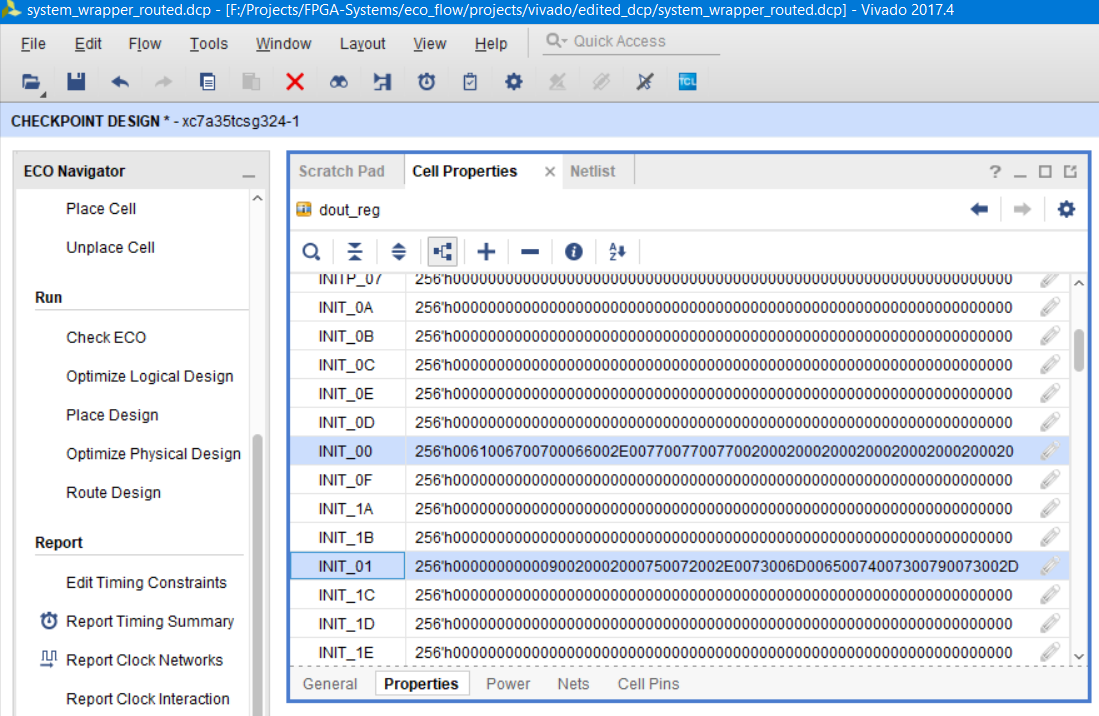
110 – INIT ASCII
, . Generate Bitstream . .ltx, (. 111).
111 –
Hardware manager FPGA .bit .ltx (.112). , edit_dcp.

112 –
, . 73-75 ( hw_ila_2, ASCII ). , . 113.

113 –
, , , , . , , , , MMCM PLL . , , , , (Report Timing Summary ..).
6.3. ILA
, ECO , . , , « ». , gnd vcc.
, , , .
ECO, , ; .
: , « », : . : , , Disconnect Net . «DONT_TOUCH» ( «unrote») – Disconnect Net . .
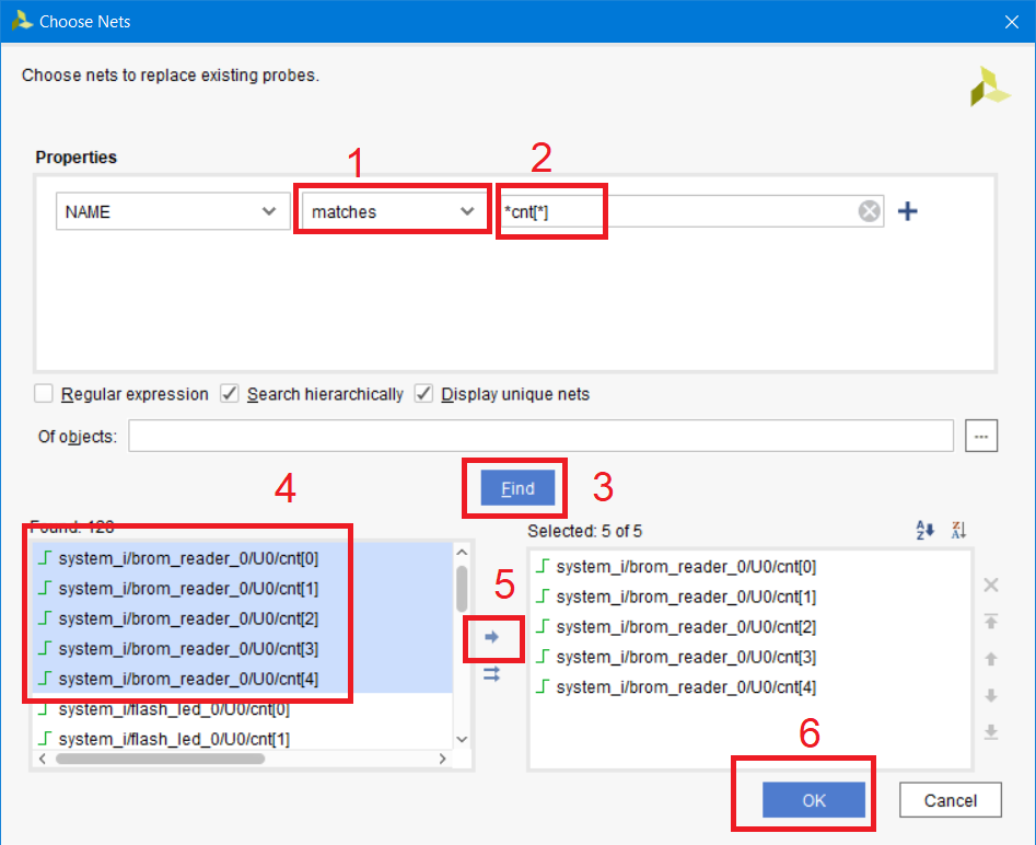
, , . , brom_reader. . , (. 114). cnt, , 5.
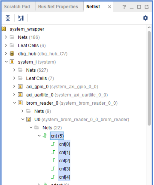
114 –
Replace Debug Probes. 31, 5 , ila_1, Edit Probes (. 115). ila, . , .
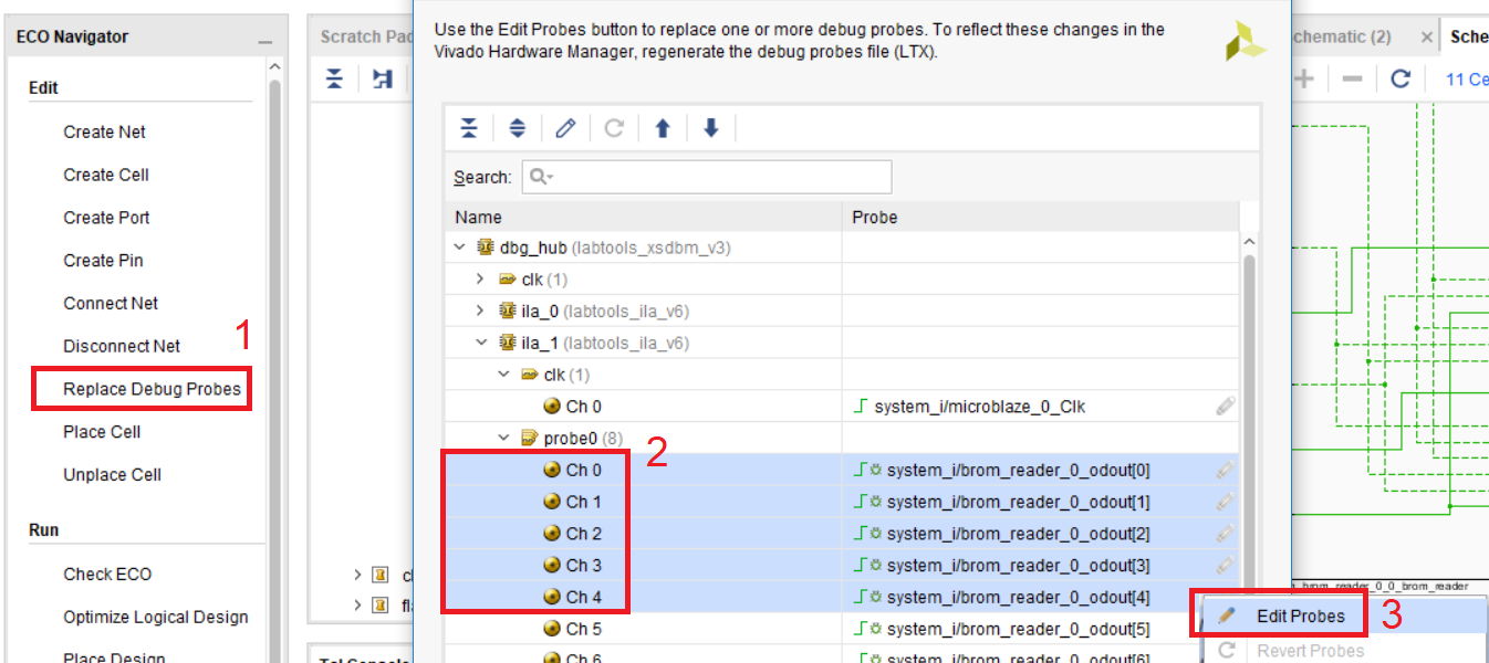
115 –
, *cnt[*]. , . , 5 , 5 . contains match tcl . Tcl , .
116 –
«0», Vivado , gnd const0. , Edit Probes (.117).

117 – ila_1
*const0 , , (. 118). !!! Debug Hub (dbg_hub), Vivado , . IP, , uartlite.
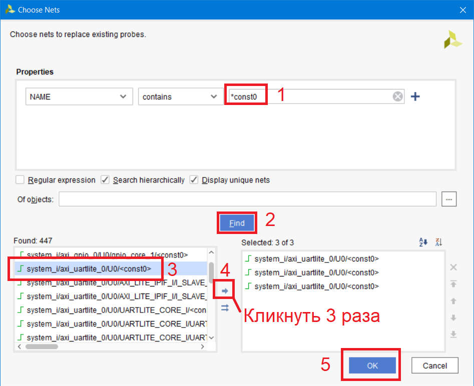
118 –
ila_1 . 119. , . , DRC.

119 – ila_1
OK , , DONT_TOUCH , ila_1. , . , , . , Unset Property DCP.
, , (.120). 1 . , !
120 –
Hardware Manger , .bit .ltx .
hw_ila_2 4 : cnt const0. cnt hex unsigned decimal ( . 75) , . , cnt 0 31 1 (.121).
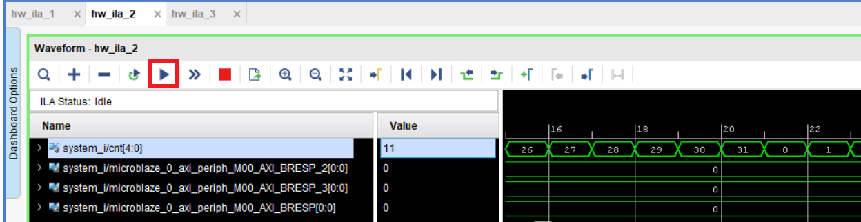
121 – cnt ila_1
, .
6.4. /
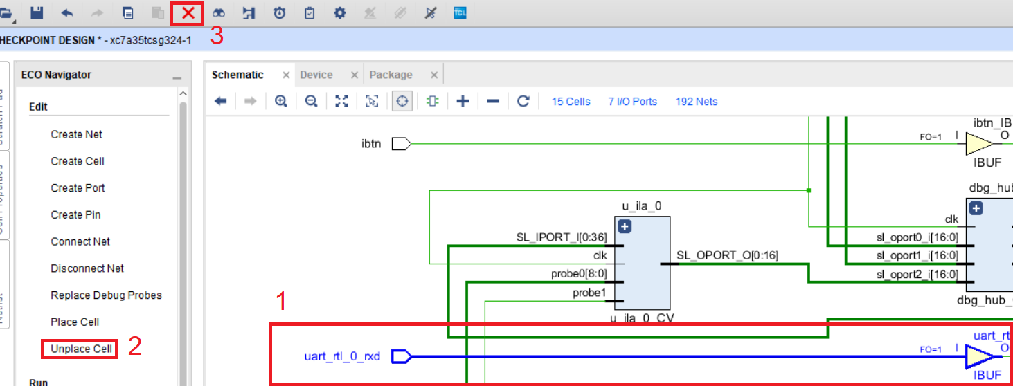
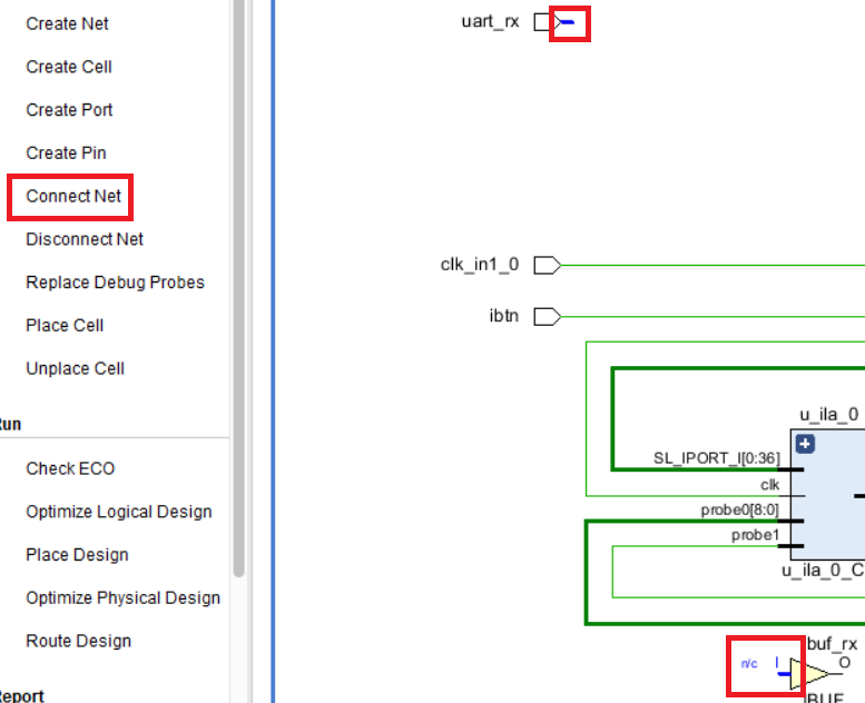
, rx tx uart - Hello World . , ECO , . .
. , , cell, . , .
.
uart_rtl_0_rxd, . unplace cell (. 122). , , .
122 –
. uart_rx, Create Port . 123

123 –
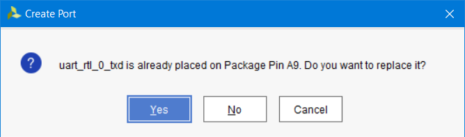
A9 , Vivado , A9. (. 124)
124 –
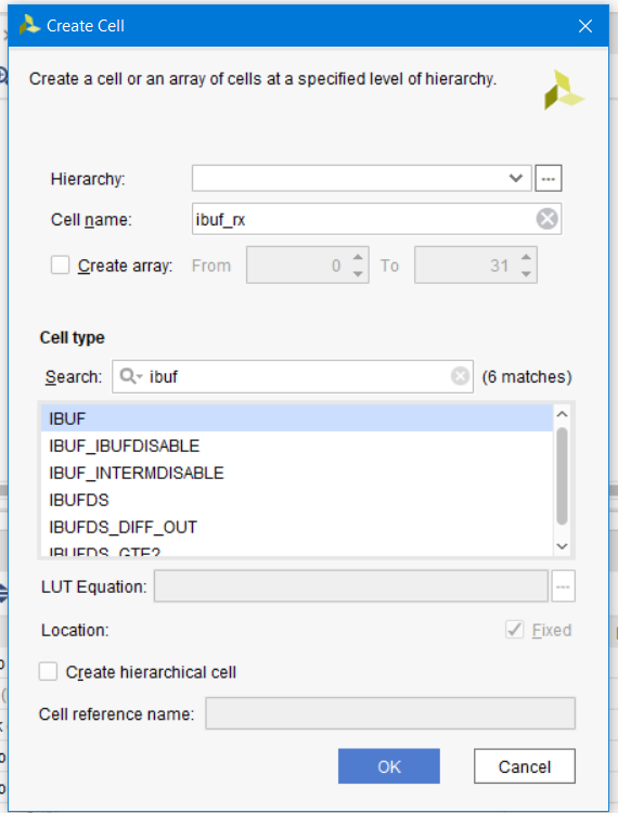
. Create Cell, ibuf_rx (. 125)
125 –
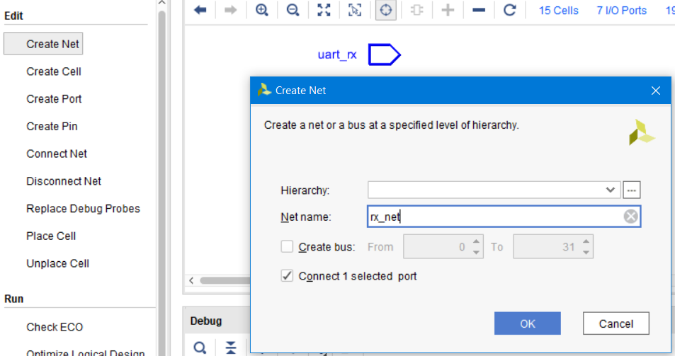
. . , . uart_rx Create Net. rx_net.
126 –
I Connect Net. (. 127)
127 –
, system_i. O uart_rtl_0_rxd, system_i Create Net
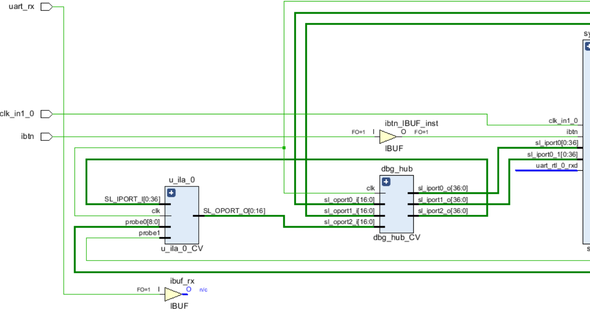
128 –
.
uart_rtl_0_txd, . Unplace cell, , (. 122). , , .

129 –
uart_tx, Create Port, Output LVCMOS33 (. 130)
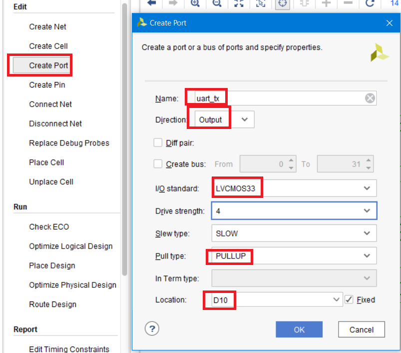
130 –
tx_net, uart_tx. uart_tx Create Net

131 – tx_net
tx_obuf, Create Cell OBUF (. 132)
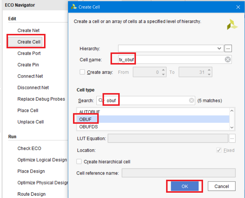
132 –
O , uart_tx Connect Net.

133 –
system_i. I uart_rtl_0_txd (. 134).

134 –
. (. 135).

135 –
Hardware Manager . SDK (. . 70). , Hello World: cycle (. 136).

136 – Hello World SDK Terminal
7.
, . , , , .. , , .. HDL , , «-» . 1. , , . , . , IP Integrator – IP RTL.
Table 1. Comparative analysis of the time spent on obtaining the final firmware file in various modes.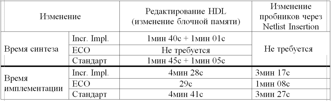
Summarizing the comparative analysis, I would say once again that it is very superficial. You understand perfectly well that FPGA is a complex system and the time of a particular stage of the design route can vary greatly. However, ECO does not require synthesis, and making small changes to the project is much faster, especially when you want to save the trace of the crystal and make changes only to the contents of the components.
8. Conclusion
Have I ever applied the ECO mode in practice? Yes. , , , . ECO; , Tcl-, . , ECO – , LogicAnalyser (ChipScope) ILA ( ) . , , - , .
ECO Flow , , : Vivado ECO Flow.
. Good luck!
9.
- , LUT, , .
- ECO. Tcl Vivado [9].
- AXI-lIte, GPIO. ECO , ila_1 uartlite, gpio.
- * , MMCM, 100. 50 . , . , , .
- * Tcl , ECO. , , , ..
- ** , brom_reader, 32 ASCII, /
1. Vivado Xilinx
2. Arty Board Digilent
3. UG904 Vivado Design Suite User Guide: Implementation
4. UG908 Vivado Design Suite User Guide Programming and Debugging
5. UG986 Vivado Design Suite Tutorial: Implementation
6. Wiki : ECO
7. UG949 UltraFast Design Methodology Guide
8. UG892 Vivado Design Suite User Guide Design Flows Overview
9. UG835 Vivado Design Suite Tcl Command Reference Guide
10. UG894 Using Tcl Scripting
11. UG901 Vivado Design Suite User Guide Synthesis
12. Arty Reference Manual
13. UG908 Programming and Debugging
14. UG1037 Vivado Design Suite AXI Reference Guide
15. Hex-to-ASCII
16. Lead: Developing a MicroBlaze software processor Xilinx Vivado IDE / HLx Environment
Appendix A. Listing of the flash_led module
library IEEE; use IEEE.STD_LOGIC_1164.ALL; entity flash_led is Port ( iclk : in STD_LOGIC; oled : out STD_LOGIC); end flash_led; architecture rtl of flash_led is signal cnt : natural range 0 to 100_000_001 := 0; signal led : std_logic := '0'; begin process(iclk) begin if rising_edge(iclk) then if cnt = 100_000_000 then cnt <= 0; else cnt <= cnt + 1; end if; if cnt < 50_000_000 then led <= '0'; else led <= '1'; end if; end if; end process; oled <= led; end rtl; Appendix B. Listing module brom_reader
library IEEE; use IEEE.STD_LOGIC_1164.ALL; use IEEE.NUMERIC_STD.ALL; entity brom_reader is Port ( iclk : in STD_LOGIC; odout : out std_logic_vector(7 downto 0) ); end brom_reader; architecture rtl of brom_reader is alias slv is std_logic_vector; type rom_type is array (0 to 31) of natural; signal rom : rom_type := ( 32 , 32, 32, 32, 97, 117, 116, 104, 111, 114, 58, 32, 75, 101, 105, 115, 78 , 49, 51, 32, 32, 32, 32, 32, 32 , 32, 32, 32, 32, 32, 32, 32 ); signal cnt : natural range 0 to rom'length-1 := 0; signal dout: slv(odout'range) := (others => '0'); attribute RAM_STYLE : string; attribute RAM_STYLE of rom : signal is "BLOCK"; begin process(iclk) begin if rising_edge(iclk) then dout <= slv(to_unsigned(rom(cnt), dout'length)); if cnt = (rom'length - 1) then cnt <= 0; else cnt <= cnt + 1; end if; end if; end process; odout <= dout; end rtl; Appendix B. Listing the helloworld program
#include "platform.h" #include "xil_printf.h" #include "xparameters.h" #include "xgpio.h" XGpio Gpio; /* The Instance of the GPIO Driver */ #define DELAY 10000000 int main() { init_platform(); int Status; volatile int Delay; int k = 0; /* Initialize the GPIO driver */ Status = XGpio_Initialize(&Gpio, XPAR_GPIO_0_BASEADDR); if (Status != XST_SUCCESS) { xil_printf("Gpio Initialization Failed\r\n"); return XST_FAILURE; } /* Loop forever blinking the LED */ while (1) { /* Set the LED to High */ XGpio_DiscreteWrite(&Gpio, 1, 1); xil_printf("Hello World: cycle %d\n\r", k); k++; /* Wait a small amount of time so the LED is visible */ for (Delay = 0; Delay < DELAY; Delay++){}; /* Clear the LED bit */ XGpio_DiscreteWrite(&Gpio, 1, 0); /* Wait a small amount of time so the LED is visible */ for (Delay = 0; Delay < DELAY; Delay++){}; } cleanup_platform(); return 0; } PS: intekus Des333 , ishevchuk , roman-yanalov 91 ( Word), .
Source: https://habr.com/ru/post/353094/
All Articles