Time-to-Digital (TDC) converters: what it is and how they are implemented in FPGA

The figure is the first in the world of the Mo-Tzu quantum communication satellite , which was launched from China in 2016, with the TDC implemented in FPGA.
To explain to his girlfriend (or boyfriend) what ADC and DAC are, and in what household appliances they are used, every person who calls himself an engineer can. But what TDC is and why we don’t have them at home can often be found only after the wedding.
TDC is a time-to-digital converter. In Russian, speaking: time-measuring system.
')
The main consumers of high-speed TDC are research groups. As a rule, something very specific is required for a specific research project. That channels need a lot, the resolution is very high, then the performance is compact. And the level of development of modern FPGAs and their availability just give researchers the opportunity to experiment with implementations and adjust them for their own needs.
In this habrastia, a detailed description of a simple time-measuring system on FPGA Cyclone IV. The article will be useful not only for expanding horizons, but also from a methodological point of view, since the implementation of the system is nontrivial.
Immediately, we note that the thought that came to mind “What are they writing about? We read the CPU / MCU counter / timer by event and it's in the bag ”is not suitable here. The fact is that applications require precision by an order of magnitude greater than can be provided by “standard” counters, as well as deterministic latency, multi-channel and large “event throughput”.
Formally, the task that TDC solves is to determine the time interval between events. In multichannel systems, top-level logic can additionally calculate correlations between events. The event is usually triggered by a particle detector or optical sensor. In everyday life, of course, such systems do not find application. And in general, on the scale of picoseconds, it makes sense to measure physical processes occurring in comparable times, for example, the passage of elementary particles in a detector. Note some areas of TDC application:
- Mass spectroscopy, positron emission tomography (PET) —the arrival times of particles at the detectors are recorded.
- LIDAR - based on time counts, the distance to the irradiated area is determined.
- Quantum cryptography - the response times of single photon detectors are recorded.
- Random number generation - the times of occurrence of events are used as entropy.
The electrical impulse generated by the detector goes through a preprocessing circuit that translates it into a “digestible” form for electronics. That is, the needle ( glitch ) turns into a signal with a duration of several nanoseconds with an amplitude of several volts. Depending on the implementation, this circuit may be located directly in the detector or in the measuring system. Below is a timing chart of the output signal of the ID Quantique single photon detector . In addition to the impulse itself, the so-called “dead time” of the detector can be seen in the picture. This is the time interval during which the detector does not respond to external events. Since this time arises from the features of electronic circuits, then the TDCs themselves have some dead time, with which developers continuously struggle.

For highly accurate measurement of time intervals, both boxed solutions and specialized ASICs are available on the market. On the topic of implementation of TDC is quite extensive material. The general theory can be found in the book Time-to-Digital Converters by Stefan Hantsler , and with various modern implementations in periodicals, for example, on arxiv.org . We will talk about a simple TDC FPGA implementation.
TDC implementation in FPGA
From an electronic point of view, the implementation of the task is reduced to “registering the position” of the signal front relative to any sync signal. The FPGA elements that we have at our disposal are physically on-chip signal lines, registers, logic blocks, clock lines, and PLL . The main approaches to the implementation of TDC using these elements were proposed relatively long ago: sub- tact delay line ( tapped delay line ), Vernier delay line ( delayed line ), “phased PLL” . But engineers are still working on their improvement and implementation on modern platforms.
In our FPGA implementation, we basically followed this publication , describing the sub-tact delay line, as well as some general ideas drawn from the Jinyuan Wu publications from CERN 2000-x.
The concept of a sub-tactical delay line is shown in the figures below (the animation is taken from the presentation of Jinyuan Wu, Z. Shi and I. Wang). Essence: to pass the input signal through the circuit formed by the delay elements, the outputs of which are connected to simultaneously latching registers. As a result, the values snapped into the register set — the thermocode — correspond to the mutual arrangement of the input fronts and the clock signals. Then everything is simple. We correct the errors in the thermocode, decode it into a number, reset the values of the registers, add the number of the cycle in which the event is registered, and pass to the output.


We recall the device FPGA Cyclone family from Intel (Altera). Logic elements ( LE ) are grouped into blocks ( LAB ), controlled by one line of the shred and connected by lines of transfer of the discharge ( carry line ). This is exactly the scheme we need. That is, the input signal will start on some LE and direct it along the lines of transfer of the discharge to the neighboring ones. At the same time LE should work in arithmetic mode. We will clock all LEs in one shred and pick up the thermocode upon the appearance of the input signal.
Now we face several practical issues:
- How to describe the delay line scheme on verilog?
- How to explain to Quartus that we want to use the transfer lines and disable their optimization?
- How to form a delay line on neighboring LEs from one LAB ?
Verilog's schema description language does not allow to describe synthesized delays. The delays specified by the #N instruction are intended for simulation. But in our case, this is not required. The key is to describe the use of LE in a specific way.
For this, the LE element IP block goes to the Intel element library. This module is common to the LE- Cyclone family, and in our case some of its parameters are not involved.
From the point of view of Quartus, the delay line is pointless. Why keep the signal tricky way, if it can be immediately carried out from point A to point B? In order for Quartus not to try to optimize the delay line, and as a result, threw out the components of its LE , we use the directive / * synthesis keep = 1 * / opposite the declaration of the element to which it relates. As a result, the main code looks like this:
// cyclone_lcell #( .operation_mode ("arithmetic" ), // «» .synch_mode ("off" ), .register_cascade_mode ("off" ), .sum_lutc_input ("datac" ), .lut_mask ("cccc" ), // «» .power_up ("low" ), .cin_used ("false" ), .cin0_used ("false" ), .cin1_used ("false" ), .output_mode ("reg_and_comb" ), // .lpm_type ("cyclone_lcell"), .x_on_violation ("off" ) ) u_cell0( /* synthesis keep = 1 */ .clk ( clk ), // .dataa ( 0 ), .datab ( in_hit ), // .datac ( 0 ), .aclr ( 0 ), .aload ( 0 ), .sclr ( 0 ), .sload ( 0 ), .ena ( 1 ), .inverta ( 0 ), .regcascin ( 0 ), .combout ( ), .regout ( r_out[0] ), // .cout ( c_out[0] ) // ); // genvar i; generate for (i = 1; i < DELAY_STAGES; i = i + 1) begin : DELAY_LINE cyclone_lcell #( .operation_mode ("arithmetic" ), // «» .synch_mode ("off" ), .register_cascade_mode ("off" ), .sum_lutc_input ("cin" ), .lut_mask ("f0f0" ), // «» .power_up ("low" ), .cin_used ("true" ), // .cin0_used ("false" ), .cin1_used ("false" ), .output_mode ("reg_and_comb" ), // .lpm_type ("cyclone_lcell"), .x_on_violation ("off" ) ) u_cell1( /* synthesis keep = 1 */ .clk ( clk ), // .dataa ( 0 ), .datab ( 0 ), .datac ( 0 ), .cin ( c_out[i-1] ), // .aclr ( 0 ), .aload ( 0 ), .sclr ( 0 ), .sload ( 0 ), .ena ( 1 ), .inverta ( 0 ), .regcascin ( 0 ), .combout ( ), .regout ( r_out[i] ), // .cout ( c_out[i] ) // ); end endgenerate To indicate the use of neighboring LEs and their placement in a specific location on a chip, use the LogicLock Regions tool. That is, let us indicate a rectangular area on the crystal and clearly indicate the set LE, which Quartus should place in it. In the figure below, the line area contains the delay line, and the delay_line area includes the additional logic for processing the thermal code.

Below is the layout of the elements of the delay line from Chip Planner with a schematic display of signals and a detailed diagram of the first two elements of the delay line.

Note that the implemented circuit has a dead time of one cycle, which is necessary for “resetting” the delay line registers.
The scheme described was decomposed on a Cyclone IV EP4CE22 chip. Experiments with the length of the delay line and the frequency of the clock resulted in the following parameters: the length of the delay line 64 LE , the frequency of the clock ~ 120 MHz. The delay line and the thermal code processing logic fit into 42 LABs .
TDC Calibration
Obviously, the physical delays on each logical element are different. To account for this fact, it is necessary to calibrate the device. The first thing that comes to mind is the input to the TDC input of a signal with a known period. However, such a path is rather laborious, since it requires precision scanning of the signal period in a relatively wide range.
The next suggestion is a random event calibration: we apply signals with uniformly distributed random delays to the input and observe a histogram of events falling into the time bin. In this case, the accuracy increases with the accumulation of events as where N is the number of events filed. We will use the method of correlated events . In this method, accuracy is limited initially and can be achieved by a relatively small number of measurements.
The essence of the method is to select the frequency of generation of events, at which they will be evenly distributed in time bins. For this, it is necessary to satisfy the relation:
where N is the number of events that we want to evenly distribute in the time interval T1, 1 / T2 is the frequency of event generation, {...} is the fractional part of the number.
In this case, signals can be generated by an internal PLL. In our example, the PLL input frequency is 50 MHz and for the number of events N = 256, we selected the following operating frequencies:
- 1 / T1 = 50 MHz * 93/40 = 116.26 MHz: clock frequency TDC
- 1 / T2 = 50 MHz * 32/285 = 5.614 MHz: frequency of event generation
The ratio is such that at approximately twenty TDC clock cycles there is one event. In this case, the resolution between adjacent events is:
The calibration procedure consists in the repeated measurement of a continuous sequence of 256 events. In our experiment, the total number of measured events is 8192. The resulting histogram corresponds to the fraction of the individual delay elements in one TDC cycle.
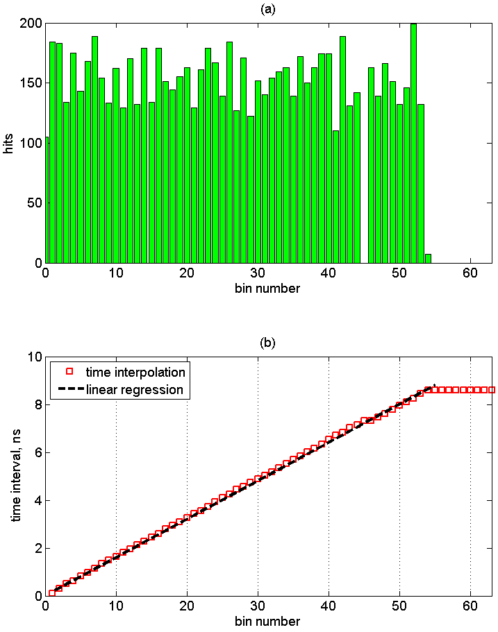
The upper graph shows the distribution of samples by the elements of the delay line. The reference number should be understood as the boundary between ones and zeros in the corrected hotcode. The failure on the 45th element of the delay line corresponds to the simultaneous operation of two adjacent elements, which is characteristic of such a realization (bubble error [Wu08]). The position of the dip depends on the area where the delay line is located on the chip. With an increase in the number of recorded events, there is no significant change in the distribution of samples.
The lower graph shows a calibration curve that compares the interval number with the delay time. The sum of all time-counting samples corresponds to the time T1 = 8.6ns. Translation of the bin number into time intervals can be carried out directly in the chip or using a programmable Nios II processor.
The following are the absolute time intervals corresponding to the elements of the delay line with a significant number of operations and the distribution of intervals. The average value of the interval is 160 ps, the time variance is 31 ps. As a result, it can be argued that the achieved resolution of the time-measuring system is ~ 200 ps . To feel this number, we note that it corresponds to the frequency of 5 GHz. And this is only the simplest implementation in FPGA, not on the very last chip!

Conclusion
We looked at some aspects of TDC implementation in FPGA. However, much of the detail is omitted. If you are interested in this topic, we advise you to get acquainted with such things as dynamic calibration; methods of error correction (bubble errors), increasing the resolution of TDC (wavelauncher), reducing the uncertainty of the interval (averaging, multiple TDC instances), reducing the dead time. You can also consider the implementation of TDC on alternative platforms.
Source: https://habr.com/ru/post/352276/
All Articles