Innovative 3D XPoint memory: technology potential and development prospects
In the previous article, we looked into the past, remembered how the SSD era began and how SSDs changed over time, transforming from bulky and often unprofitable devices into a must-have for any professional and enthusiast. It is time to look into the future: today we will talk about 3D XPoint - non-volatile memory developed by Intel and Micron. What are the capabilities of the chips and is the new technology really able to turn the industry upside down? Let's try to figure it out together.
Although Intel refuses to tell the world exactly which physical processes underlie the new chips, based on published data, we can conclude that the origins of 3D XPoint lie in the 1960s: the technology is based on the achievements of American scientist Stanford Ovshinsky, who registered over 400 patents in his lifetime in the field of energy and information technology. His invention was called PRAM (Phase-change memory - phase transition memory).

Stanford Ovshinsky, inventor of PRAM
Unlike flash memory, PRAM uses binary chalcogen chemical compounds in amorphous (value “0”) and crystalline (value “1”) states to represent binary values. The physical basis of this approach is the cardinal difference in the electrical resistance of chalcogenides, depending on the state of matter in the aggregate, while the flash memory works due to a change in charge on the floating gate. Depending on the level of the latter, the threshold voltage of the transistor also changes, becoming higher or lower and encoding thus 1 or 0. To record a different value, it is necessary to initiate a discharge of the accumulated charge, however, to “pull” electrons from the floating gate, a relatively high voltage is required in turn, is achieved through the swap process. Since the accumulation of energy requires a certain time, the flash memory turns out to be rather “slow”: in comparison with the same SRAM, the read time of the data block is almost 100 thousand times longer. PRAM, on the other hand, is devoid of this disadvantage, since the values of individual bits can be changed without first erasing the information.
')
That PRAM and formed the basis of 3D XPoint. As the name implies (XPoint should be read as a crosspoint, which means “intersection”), the memory crystals of the new sample received a cross-structure.
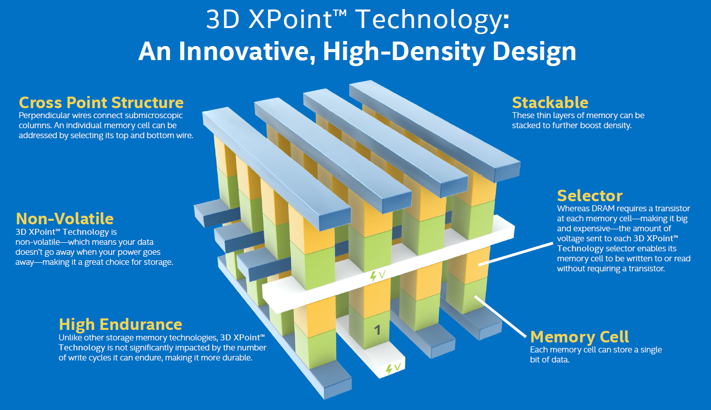
XPoint 3D structure
A pair of "selector - memory cell" is located at the intersection of perpendicular conductors. The selector is activated when a voltage of a certain value is applied, and the aggregate state of the substance in the cell changes and a bit is recorded. Since the addressing occurs without the participation of transistors, this has significantly reduced the area of the crystal, increasing the storage density: according to the developers, the gain is 4 to 10 times compared to DRAM.
The first generation of XPoint 3D chips is performed on a 20-nanometer process technology, and the chips themselves are dual-layered. With the transition to EUV-lithography, it will be possible to complicate production up to 10 nm, and the structure will grow in three dimensions, which will help to significantly increase the capacity of the chips, as well as speed up the reading / writing process. There is also the prospect of storing two bits in one cell due to the use of boundary states of a substance, each of which has its own electrical characteristics. Such studies have already been carried out by Intel and ST Microelectronics, although they are still far from being implemented in commercial products.
Despite all the advantages, non-volatile PRAM, which also includes 3D XPoint, has weaknesses. Among them, one should focus on the direct contact of the phase transition region and the dielectric, which with time can lead to the detachment of the latter and provoke a charge leak. Another nuance is the increase in the resistance of chalcogenides, which is described by the power law ~ t ^ 0.1. In multilevel structures, this can lead to mixing of the lower and upper layers of the substance in an intermediate state, which makes the chips sensitive to the slightest deviations from the threshold voltage values. Obviously, Intel was able to solve these problems by making the crystal more stable, but the details of the technology were not disclosed.
All of the above looks very tasty, but you can understand how good 3D XPoint is in real-world scenarios only if you have ready devices in your hands. And those already exist: March 20, 2017, Intel introduced a line of drives based on innovative memory, called the Optane SSD DC P4800X format PCI Express HHHL. The devices use 128-gigabit 20-nanometer 3D XPoint chips, have a capacity of 375 or 750 GB and are equipped with an Intel NVMe ASIC controller, which is able to control four crystals on one channel at the same time, which provides phenomenal performance: when processing 4 KB blocks, the performance of the device reaches 550,000 IOPS when reading and 500,000 IOPS when writing, and the delay does not exceed 10 µs. The maximum sequential read speed reaches 2400 MB / s, and the recording speed is 2000 MB / s. The Optane resource is also quite high: Intel declares about 12.3 PB of overwriting.
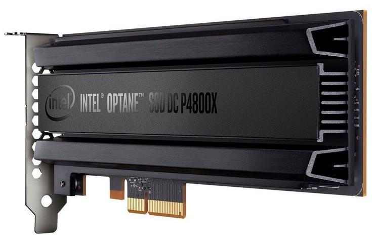
Intel Optane SSD DC P4800X
Impressive? Indisputable! But do not rush to place orders: the recommended price of Optane is 1520 US dollars, as of February 2018, the cost of storage in Russia varies from 106 to 118 thousand rubles. All this recalls the release of the Axlon RAM Disk for the Apple II, which turned out to be a hundred bucks more expensive than the computer itself (we wrote about this and other interesting devices in the article “The Evolution of Solid-State Drives: From the First Models of the 70s to the Present Day ”), with the only difference is that the brainchild of Intel is focused on the corporate sector and knowledge-intensive industries, where the speed of information processing comes to the fore.
Are there consumer-grade solutions based on 3D XPoint? Yes. The product is called Intel Optane Memory and comes in two versions: 16 GB (the average price is about 3200 rubles) and 32 GB (5100 rubles). Both drives are NVMe SSDs made in the M.2 2280-S3-BM form factor and are characterized by the following parameters:
The figures (as well as the cost of one gigabyte) are not encouraging, but Intel Optane Memory is not positioned as a full-fledged solid-state drive, but as a sort of “HDD accelerator”, and moreover, not for everyone. Seventh-generation or older processor, Intel 200 Series chipset or newer, BIOS with UEFI-driver RST 15.5 or higher, Windows 10. Got a platform for Ryzen, still sitting on Core i7 2700 or are you a Linux fan? In this case, this technology is not for you. And even if your car fully complies with the listed requirements, do not rush to purchase.
Due to the small size and the peculiarities of the caching algorithm, the device can provide some noticeable acceleration only when the operating system is loaded and some fixed set of applications is used. At the same time, content makers simply will not notice a performance boost, since Intel Optane Memory ignores operations with multimedia files (the driver checks the extensions) due to limited capacity. Installation and updating of programs will also be carried out at the same speed, because executable files are sent to the cache, to which there were at least three consecutive calls, and the installers are run once. Will this solution appeal to avid gamers? Taking into account the fact that the available space is five times less than in the "weight" of modern AAA games, the answer is obvious.
However, if we again turn to history, a similar situation was observed with flash memory, when the first retail product (IBM DiskOneKey flash drive) came out only 10 years after the advent of technology. Perhaps something similar will happen with 3D Xpoint: after some time, the cost of chips will decrease and anyone can buy a model of DC P4800X level at an adequate price?
Guy Bleloc, director of IM Flash (a joint venture founded by Intel and Micron in 2006), commented on the pricing of new devices, giving an interview to the well-known industry publication EE Times. According to him, in the near future, full-fledged consumer-class drives using 3D XPoint memory are definitely not worth waiting for, or maybe they will never appear at all.

Guy Blelock, IM Flash Director
There are a number of completely objective reasons for this. One of them is that in order to create new chips, over 100 names of raw materials are needed, and some positions are so unique that they are produced by a single company in the world. This, in turn, causes problems with attracting investment. “For many investors, this state of affairs is unacceptable - they want to be sure of uninterrupted supplies in case of force majeure,” said Bleok.
Another problem is due to the peculiarities of the technological process. The release of XPoint 3D requires additional steps in the production chain, as the cross-architecture increases the risk of mutual contamination of the materials that make up the cells. Such complex stages as vacuum deposition and evaporation are added, which entails a significant decrease in the productivity of factories, and this is already reflected in the cost of finished devices. Although it is possible to compensate for the reduction in production volumes, pleasure is extremely expensive even for such a large corporation as Intel.
According to preliminary calculations, the number of plates produced will need to be increased from 180 to 1000 per hour per conditional 2 square meters of space. Considering that at this stage in the development of technology, it is practically impossible to increase the density of production, for a fivefold increase in capacity, the plant itself will have to be expanded at least 5 times, which will entail serious capital expenditures. The most unpleasant thing is that the further transition to 3D XPoint of the second and third generations will require comparable investments. And here the advantages of 3D NAND memory become obvious, in the case of which the change of technical process leads to an increase in costs only within 20-30%.
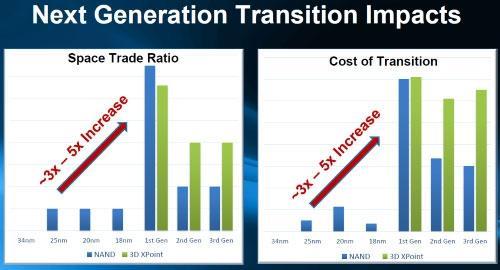
Comparing the cost of upgrading 3D NAND and 3D XPoint production
In addition, Guy Blanque noted that 3D XPoint is extremely difficult to scale. It is theoretically possible to create even four-layer chips, however, for their mass production, EUV-scanners of extreme ultraviolet lithography are needed, whose commercial versions simply do not exist. All of the above are serious constraints for the further evolution of the technology, so in the short term, it is not necessary to dream about the price of 3D XPoint drives to an acceptable level.
There is one more nuance that not everyone paid attention to. Currently, the warranty period for new Optane is 3 years, but in the future the corporation promises to increase it to 5 years. As a rule, such a significant variation indicates the absence of sufficient statistical data on the basis of which one can judge the frequency of occurrence of malfunctions or the complete failure of equipment. And this can only mean one thing: it’s too early to talk about the reliability and fault tolerance of 3D XPoint drives, and the 12.3 PBW figure is actually less capable.
Fortunately, it is still a bit early to bury the classic NAND, because the planar chips were replaced by vertical three-dimensional ones, and their appearance was due not only to the need to meet the growing needs of IT, but also to economic feasibility. Turning to a 14-nanometer process, flash memory manufacturers are at a crossroads. Increasing the density of the crystal would require a complete modernization of production, therefore, where investment in further scientific research turned out to be more profitable, the result of which was the creation of multilayer chips.
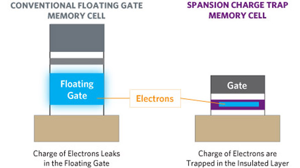
Recall that the basis of NAND-memory transistors with a floating gate, capable of holding the charge for a long time. Reducing their size is fraught with leaks from one cell to another, which may result in damage to the stored data. A similar problem arises when attempting to build three-dimensional clusters; however, it turns out to be much easier to solve: it is enough to create an isolated region from a non-conductive substance, where the charge will be stored. The technology was named CTF (Charge Trap Flash - “trap for charging”), and silicon nitride (SiN) was used as the material for the insulating layer.
CTF device
Unlike planar chips, in 3D NAND each cell is represented by a multi-layer cylinder. Its outer layer is nothing more than a control gate, while the inner layer is an insulator. Placed at each other cells form a stack, along the axis of which passes a common channel of polycrystalline silicon. Thus, the number of cells in the stack is equal to the number of layers in the crystal.
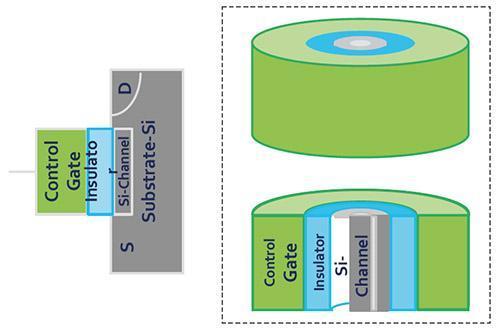
The principle of the device cells in 3D NAND
This architecture provides a number of key benefits:
With the efforts of SanDisk, now owned by Western Digital, 3D NAND technology has been further developed. The principle of its device remained the same, but the linear lines were replaced by U-shaped ones. In this case, the switching transistor and the source line were moved to the upper part of the sequence, which made it possible to eliminate the probability of their damage due to high temperatures and, thus, reduce the number of errors during read / write operations.
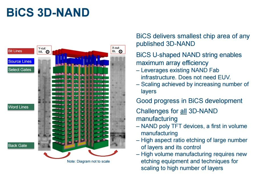
3D NAND BiCS Scheme
The new generation of 3D NAND is called BiCS, which stands for Bit Cost Scalable, and this name turned out to be quite justified. After all, this technology allowed us to create high-capacity 64-layer chips based on well-established 40-nanometer production, thereby eliminating the need for expensive photolithography in the deep ultraviolet (EUV).
3D NAND BiCS formed the basis of affordable and productive solutions focused on the private consumer. In August 2017, Western Digital switched to the production of solid-state SATA drives based on the latest generation of three-dimensional chips, and now we are pleased to offer our customers an updated line of SSD Blue. Although 3D NAND BiCS is slower than 3D XPoint, in terms of price and quality, this offer is the best on the market. The numbers below speak for themselves.
A wide range of models allows you to choose the option that fully meets your needs. For those who want to increase the speed of the computer, a 250 GB SSD is enough to accommodate the operating system and installed software. If you are a content maker and not only speed, but also the available volume is important to you, we recommend to pay attention to the flagship of the 2-TB Blue-series. As for fault tolerance, even with a daily load of up to 80 GB of rewriting, the drives will work for at least 7 years, a record figure for devices of this class.
For those who do not tolerate compromises and want to squeeze the most out of their own PC or laptop, we have prepared high-speed WD Black SSD based on planar chips, the performance of which was significantly increased by using the PCIe Gen3 NVMe interface with a throughput of 8 Gb / s. In the overwhelming majority of highly loaded scenarios (3D modeling, video coding, heavy video games and VR), the WD Black potential is more than enough: SSDs show a stable speed of 2050 MB / s with sequential read and 800 MB / s with sequential writing, as well as up to 170,000 IOPS with random read and up to 130,000 IOPS with random write (4 KB blocks). The drives are available in two versions: 256 and 512 GB.
At the moment, it is still too early to talk about a complete rethinking of the approach to creating solid-state drives. On the contrary, there are prerequisites for market segmentation: if 3D XPoint can dominate the corporate sector, then 3D NAND is confidently developing retail. Due to the high cost of decisions based on the descendant of PRAM, there can be no talk of any kind of confrontation, especially since such performance is redundant for most household and professional tasks, and therefore, given the price, the end user does not receive any significant benefits. Most likely, both technologies will develop in parallel, without competing with each other until something fundamentally new appears in the depths of research laboratories. But when the next breakthrough happens, one can only guess.
Although Intel refuses to tell the world exactly which physical processes underlie the new chips, based on published data, we can conclude that the origins of 3D XPoint lie in the 1960s: the technology is based on the achievements of American scientist Stanford Ovshinsky, who registered over 400 patents in his lifetime in the field of energy and information technology. His invention was called PRAM (Phase-change memory - phase transition memory).
Stanford Ovshinsky, inventor of PRAM
Unlike flash memory, PRAM uses binary chalcogen chemical compounds in amorphous (value “0”) and crystalline (value “1”) states to represent binary values. The physical basis of this approach is the cardinal difference in the electrical resistance of chalcogenides, depending on the state of matter in the aggregate, while the flash memory works due to a change in charge on the floating gate. Depending on the level of the latter, the threshold voltage of the transistor also changes, becoming higher or lower and encoding thus 1 or 0. To record a different value, it is necessary to initiate a discharge of the accumulated charge, however, to “pull” electrons from the floating gate, a relatively high voltage is required in turn, is achieved through the swap process. Since the accumulation of energy requires a certain time, the flash memory turns out to be rather “slow”: in comparison with the same SRAM, the read time of the data block is almost 100 thousand times longer. PRAM, on the other hand, is devoid of this disadvantage, since the values of individual bits can be changed without first erasing the information.
')
That PRAM and formed the basis of 3D XPoint. As the name implies (XPoint should be read as a crosspoint, which means “intersection”), the memory crystals of the new sample received a cross-structure.
XPoint 3D structure
A pair of "selector - memory cell" is located at the intersection of perpendicular conductors. The selector is activated when a voltage of a certain value is applied, and the aggregate state of the substance in the cell changes and a bit is recorded. Since the addressing occurs without the participation of transistors, this has significantly reduced the area of the crystal, increasing the storage density: according to the developers, the gain is 4 to 10 times compared to DRAM.
The first generation of XPoint 3D chips is performed on a 20-nanometer process technology, and the chips themselves are dual-layered. With the transition to EUV-lithography, it will be possible to complicate production up to 10 nm, and the structure will grow in three dimensions, which will help to significantly increase the capacity of the chips, as well as speed up the reading / writing process. There is also the prospect of storing two bits in one cell due to the use of boundary states of a substance, each of which has its own electrical characteristics. Such studies have already been carried out by Intel and ST Microelectronics, although they are still far from being implemented in commercial products.
Despite all the advantages, non-volatile PRAM, which also includes 3D XPoint, has weaknesses. Among them, one should focus on the direct contact of the phase transition region and the dielectric, which with time can lead to the detachment of the latter and provoke a charge leak. Another nuance is the increase in the resistance of chalcogenides, which is described by the power law ~ t ^ 0.1. In multilevel structures, this can lead to mixing of the lower and upper layers of the substance in an intermediate state, which makes the chips sensitive to the slightest deviations from the threshold voltage values. Obviously, Intel was able to solve these problems by making the crystal more stable, but the details of the technology were not disclosed.
Intel Optane SSD DC P4800X - the first commercial 3D XPoint drive
All of the above looks very tasty, but you can understand how good 3D XPoint is in real-world scenarios only if you have ready devices in your hands. And those already exist: March 20, 2017, Intel introduced a line of drives based on innovative memory, called the Optane SSD DC P4800X format PCI Express HHHL. The devices use 128-gigabit 20-nanometer 3D XPoint chips, have a capacity of 375 or 750 GB and are equipped with an Intel NVMe ASIC controller, which is able to control four crystals on one channel at the same time, which provides phenomenal performance: when processing 4 KB blocks, the performance of the device reaches 550,000 IOPS when reading and 500,000 IOPS when writing, and the delay does not exceed 10 µs. The maximum sequential read speed reaches 2400 MB / s, and the recording speed is 2000 MB / s. The Optane resource is also quite high: Intel declares about 12.3 PB of overwriting.
Intel Optane SSD DC P4800X
Impressive? Indisputable! But do not rush to place orders: the recommended price of Optane is 1520 US dollars, as of February 2018, the cost of storage in Russia varies from 106 to 118 thousand rubles. All this recalls the release of the Axlon RAM Disk for the Apple II, which turned out to be a hundred bucks more expensive than the computer itself (we wrote about this and other interesting devices in the article “The Evolution of Solid-State Drives: From the First Models of the 70s to the Present Day ”), with the only difference is that the brainchild of Intel is focused on the corporate sector and knowledge-intensive industries, where the speed of information processing comes to the fore.
Are there consumer-grade solutions based on 3D XPoint? Yes. The product is called Intel Optane Memory and comes in two versions: 16 GB (the average price is about 3200 rubles) and 32 GB (5100 rubles). Both drives are NVMe SSDs made in the M.2 2280-S3-BM form factor and are characterized by the following parameters:
Volume, GB | 32 | sixteen |
Sequential read speed, MB / s | 1350 | 900 |
Sequential write speed, MB / s | 290 | 145 |
Random read speed, IOPS | 240,000 | 190,000 |
Random write speed, IOPS | 65,000 | 35,000 |
The figures (as well as the cost of one gigabyte) are not encouraging, but Intel Optane Memory is not positioned as a full-fledged solid-state drive, but as a sort of “HDD accelerator”, and moreover, not for everyone. Seventh-generation or older processor, Intel 200 Series chipset or newer, BIOS with UEFI-driver RST 15.5 or higher, Windows 10. Got a platform for Ryzen, still sitting on Core i7 2700 or are you a Linux fan? In this case, this technology is not for you. And even if your car fully complies with the listed requirements, do not rush to purchase.
Due to the small size and the peculiarities of the caching algorithm, the device can provide some noticeable acceleration only when the operating system is loaded and some fixed set of applications is used. At the same time, content makers simply will not notice a performance boost, since Intel Optane Memory ignores operations with multimedia files (the driver checks the extensions) due to limited capacity. Installation and updating of programs will also be carried out at the same speed, because executable files are sent to the cache, to which there were at least three consecutive calls, and the installers are run once. Will this solution appeal to avid gamers? Taking into account the fact that the available space is five times less than in the "weight" of modern AAA games, the answer is obvious.
However, if we again turn to history, a similar situation was observed with flash memory, when the first retail product (IBM DiskOneKey flash drive) came out only 10 years after the advent of technology. Perhaps something similar will happen with 3D Xpoint: after some time, the cost of chips will decrease and anyone can buy a model of DC P4800X level at an adequate price?
Too complicated and too expensive
Guy Bleloc, director of IM Flash (a joint venture founded by Intel and Micron in 2006), commented on the pricing of new devices, giving an interview to the well-known industry publication EE Times. According to him, in the near future, full-fledged consumer-class drives using 3D XPoint memory are definitely not worth waiting for, or maybe they will never appear at all.
Guy Blelock, IM Flash Director
There are a number of completely objective reasons for this. One of them is that in order to create new chips, over 100 names of raw materials are needed, and some positions are so unique that they are produced by a single company in the world. This, in turn, causes problems with attracting investment. “For many investors, this state of affairs is unacceptable - they want to be sure of uninterrupted supplies in case of force majeure,” said Bleok.
Another problem is due to the peculiarities of the technological process. The release of XPoint 3D requires additional steps in the production chain, as the cross-architecture increases the risk of mutual contamination of the materials that make up the cells. Such complex stages as vacuum deposition and evaporation are added, which entails a significant decrease in the productivity of factories, and this is already reflected in the cost of finished devices. Although it is possible to compensate for the reduction in production volumes, pleasure is extremely expensive even for such a large corporation as Intel.
According to preliminary calculations, the number of plates produced will need to be increased from 180 to 1000 per hour per conditional 2 square meters of space. Considering that at this stage in the development of technology, it is practically impossible to increase the density of production, for a fivefold increase in capacity, the plant itself will have to be expanded at least 5 times, which will entail serious capital expenditures. The most unpleasant thing is that the further transition to 3D XPoint of the second and third generations will require comparable investments. And here the advantages of 3D NAND memory become obvious, in the case of which the change of technical process leads to an increase in costs only within 20-30%.
Comparing the cost of upgrading 3D NAND and 3D XPoint production
In addition, Guy Blanque noted that 3D XPoint is extremely difficult to scale. It is theoretically possible to create even four-layer chips, however, for their mass production, EUV-scanners of extreme ultraviolet lithography are needed, whose commercial versions simply do not exist. All of the above are serious constraints for the further evolution of the technology, so in the short term, it is not necessary to dream about the price of 3D XPoint drives to an acceptable level.
There is one more nuance that not everyone paid attention to. Currently, the warranty period for new Optane is 3 years, but in the future the corporation promises to increase it to 5 years. As a rule, such a significant variation indicates the absence of sufficient statistical data on the basis of which one can judge the frequency of occurrence of malfunctions or the complete failure of equipment. And this can only mean one thing: it’s too early to talk about the reliability and fault tolerance of 3D XPoint drives, and the 12.3 PBW figure is actually less capable.
3D NAND - the best combination of price and performance
Fortunately, it is still a bit early to bury the classic NAND, because the planar chips were replaced by vertical three-dimensional ones, and their appearance was due not only to the need to meet the growing needs of IT, but also to economic feasibility. Turning to a 14-nanometer process, flash memory manufacturers are at a crossroads. Increasing the density of the crystal would require a complete modernization of production, therefore, where investment in further scientific research turned out to be more profitable, the result of which was the creation of multilayer chips.
Recall that the basis of NAND-memory transistors with a floating gate, capable of holding the charge for a long time. Reducing their size is fraught with leaks from one cell to another, which may result in damage to the stored data. A similar problem arises when attempting to build three-dimensional clusters; however, it turns out to be much easier to solve: it is enough to create an isolated region from a non-conductive substance, where the charge will be stored. The technology was named CTF (Charge Trap Flash - “trap for charging”), and silicon nitride (SiN) was used as the material for the insulating layer.
CTF device
Unlike planar chips, in 3D NAND each cell is represented by a multi-layer cylinder. Its outer layer is nothing more than a control gate, while the inner layer is an insulator. Placed at each other cells form a stack, along the axis of which passes a common channel of polycrystalline silicon. Thus, the number of cells in the stack is equal to the number of layers in the crystal.
The principle of the device cells in 3D NAND
This architecture provides a number of key benefits:
- By increasing the number of cells per unit area, the data storage density increases and, as a result, it becomes possible to create more capacious drives.
- The read / write speed can be significantly increased, since the interference between the cells is practically absent. Due to this, when saving and reading data, only one operation is performed instead of three (there is no need for additional verification).
- 3D NAND lasts much longer, since recording does not require high voltage.
With the efforts of SanDisk, now owned by Western Digital, 3D NAND technology has been further developed. The principle of its device remained the same, but the linear lines were replaced by U-shaped ones. In this case, the switching transistor and the source line were moved to the upper part of the sequence, which made it possible to eliminate the probability of their damage due to high temperatures and, thus, reduce the number of errors during read / write operations.
3D NAND BiCS Scheme
The new generation of 3D NAND is called BiCS, which stands for Bit Cost Scalable, and this name turned out to be quite justified. After all, this technology allowed us to create high-capacity 64-layer chips based on well-established 40-nanometer production, thereby eliminating the need for expensive photolithography in the deep ultraviolet (EUV).
3D NAND BiCS formed the basis of affordable and productive solutions focused on the private consumer. In August 2017, Western Digital switched to the production of solid-state SATA drives based on the latest generation of three-dimensional chips, and now we are pleased to offer our customers an updated line of SSD Blue. Although 3D NAND BiCS is slower than 3D XPoint, in terms of price and quality, this offer is the best on the market. The numbers below speak for themselves.
Series | WD Blue SSD | |||
Form factor | 2.5ʺ, 7 mm / M.2 2280 | |||
Interface | SATA 6 Gb / s | |||
Capacity | 250 GB | 500 GB | 1 TB | 2 TB |
Sequential read speed, MB / s | Up to 560 | |||
Sequential write speed, MB / s | Up to 540 | |||
Random read speed (4 KB blocks), IOPS | Up to 95,000 | |||
Random write speed (4 KB blocks), IOPS | Up to 85,000 | |||
TBW, TB | Up to 500 | |||
MTTF, million h | Up to 1.75 | |||
A wide range of models allows you to choose the option that fully meets your needs. For those who want to increase the speed of the computer, a 250 GB SSD is enough to accommodate the operating system and installed software. If you are a content maker and not only speed, but also the available volume is important to you, we recommend to pay attention to the flagship of the 2-TB Blue-series. As for fault tolerance, even with a daily load of up to 80 GB of rewriting, the drives will work for at least 7 years, a record figure for devices of this class.
For those who do not tolerate compromises and want to squeeze the most out of their own PC or laptop, we have prepared high-speed WD Black SSD based on planar chips, the performance of which was significantly increased by using the PCIe Gen3 NVMe interface with a throughput of 8 Gb / s. In the overwhelming majority of highly loaded scenarios (3D modeling, video coding, heavy video games and VR), the WD Black potential is more than enough: SSDs show a stable speed of 2050 MB / s with sequential read and 800 MB / s with sequential writing, as well as up to 170,000 IOPS with random read and up to 130,000 IOPS with random write (4 KB blocks). The drives are available in two versions: 256 and 512 GB.
Instead of conclusion
At the moment, it is still too early to talk about a complete rethinking of the approach to creating solid-state drives. On the contrary, there are prerequisites for market segmentation: if 3D XPoint can dominate the corporate sector, then 3D NAND is confidently developing retail. Due to the high cost of decisions based on the descendant of PRAM, there can be no talk of any kind of confrontation, especially since such performance is redundant for most household and professional tasks, and therefore, given the price, the end user does not receive any significant benefits. Most likely, both technologies will develop in parallel, without competing with each other until something fundamentally new appears in the depths of research laboratories. But when the next breakthrough happens, one can only guess.
Source: https://habr.com/ru/post/350104/
All Articles