Examination of internal FPGA defects: we are looking for a black cat in a dark room
Season 2: The board contains 4 XC7K160T crystals, which do not work for more than 2-3 weeks. What is the reason for failure? We understand
1. Software.
A check was made of the number of LUT elements between the triggers. She showed it
the number reaches 12, however this does not lead to large time delays and is easy
fits in 4 ns, and even almost always in 3 ns. In the process of obtaining the result of combinatorial operations (addition and comparison of multi-digit numbers) there is a danger of increased current consumption and local heating due to the significant spread of the propagation times of pulses, and as a result, the appearance of limit switching frequencies up to 1 GHz. In Figure 1 below you can see that not one switch occurs at each clock cycle, but several.
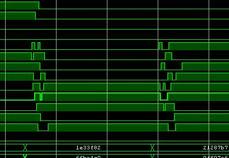
Pic1
Therefore, an attempt was made to use a conveyor for computing and estimating with
using simulation at the GATE level. There were not too many switches, and
pipelining only led to an increase in current consumption, so it was no longer applied. Evaluation of the code has shown that it is written as optimally as possible. Any changes in particular to the algorithm (for example, approximation by multiplication, which is applicable when dividing by a fixed constant) can only lead to an increase in the resources used. Therefore, the further concerned mainly search for the causes of failure of the chips.
')
2. Checking the temperature.
One of the reasons for the failure of the crystal may be overheating. The critical temperature of the crystal can be considered the temperature of more than 80 degrees. According to the expert (Novomar), silicon is “degraded”. Usually, this is how tests for the failure of crystals are carried out. In a short time, it is possible to estimate how much a crystal will work under normal conditions. Temperature measurements showed that under the worst conditions and long-term operation, temperatures above 70 degrees do not rise. (See Fig.2) From which it follows that even with a clock frequency of 300 MHz, the life of the crystal can hardly be reduced. The figure shows a graph when the calculation does not last long. It was checked that in the long-term mode the temperature above 70 degrees does not rise either.

Pic2
3. The current consumption of the core and vias.
The core current consumption (VCCINT and VCCBRAM) FPGA was measured. Power supply 1.0V.
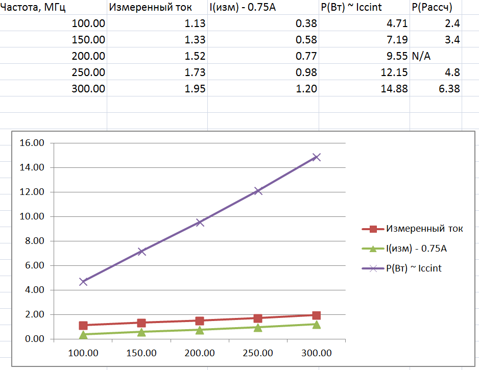
Figure 3 shows a graph of the current consumption of the core from the clock frequency of the processing unit.
data. Real and calculated. Calculated less because the mode is no computing and
computation mode is averaged. Here you can see that the current can reach values up to 15 A, while
Power contacts for FPGA 21 pcs. so The current of each pin will be approximately 0.7 A. There are 2 places in the seal (M14, N13 and L13, K12), where there are 2 pins per transition hole. So current
will be 1.4 A. The calculated value for the transition hole 1.5 A, recommended by the developers - 1 A. The test of these holes for current destruction was carried out.
A prolonged 4 A current test (several hours) had no effect on the via. Its resistance amounted to several mOhm. In addition, on the board with the FPGA removed, all the holes were checked for breaks that were not detected. The conclusion is that for this reason, the redeployment board does not need. The reason for the failure of the crystals is not that. Figure 3 shows a graph of the power consumption of the core, but since the voltage
power supply core 1 V, then the current is numerically equal to the power.
Pic.3
4. The sequence of supplying power to the crystal.
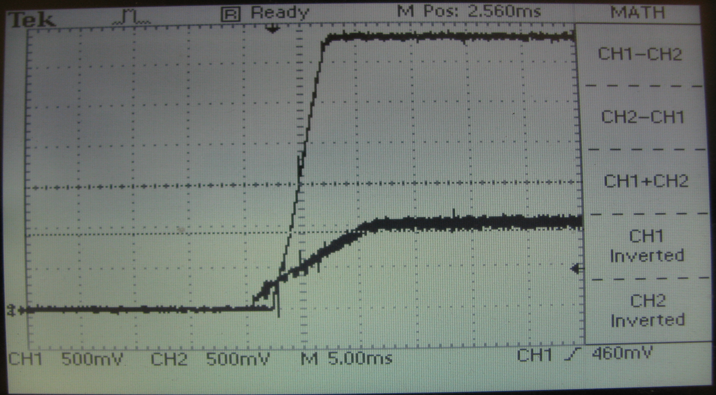
The sequence of powering the crystal is: VCCINT-> VCCBRAM-> VCCAUX &
VCCO; VCCINT and VCCBRAM are allowed at the same time. In this project, the sequence is broken. This can be seen on the oscillogram in Figure 4. For 5 ms
VCCO 3.3 V voltage exceeds 1.5 V, and VCCINT has not yet reached the nominal value. it
not recommended by the manufacturer.
Pic.4
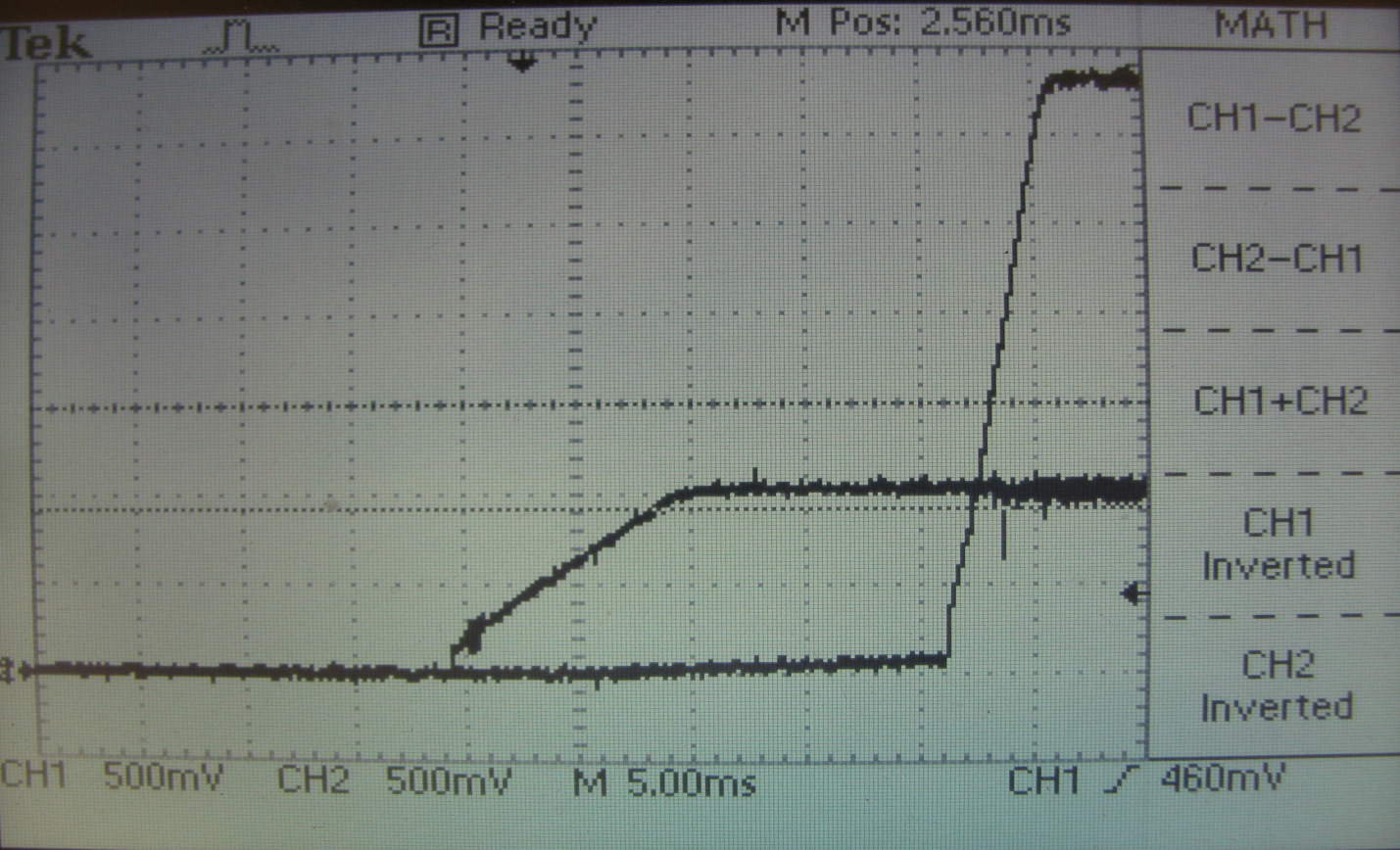
However, in this situation, failure is possible at the time of power-up. And really
crystal fails during long work. However, it is recommended to
INHIBIT contacts of 3.3 V and 1.8 V stabilizers; set 1.0 μF capacitors to GND. it
will allow them to run for a few milliseconds, and ensure that the requirement is met
power up sequences. See fig. five.
Pic.5
5. Principle diagram
The study of the circuit showed that the pin M12 VCCADC is supplied with power 3.3 V. This violates
The maximum permissible values for a crystal that makes up for this pin is 2.0 V, nominal 1.8 V. It is necessary either to redistribute the board and connect this pin to 1.8 V, or reduce the power of 3.3 V to 1.8 V. But then you need to switch the signal CFGBVS_0 to GND. It can also change other modes, so it seems better to repack.
6. Examining the state of defective crystals.
A problem with a reset has been detected on a good device. Those. when turned on, all the LEDs are lit and the device does not go into operating mode. The problem was overcome by removing the external reset and generating it inside the crystal. However, on a faulty sample, there is a problem on 3 chips out of four. On two of them, the internal RST signal does not react at all to a pin (J26) state change, on one it responds only if it is closed to ground, and so it has state 1, although it should be 0. And only on one it works correctly. This suggests that something is the result of exposure to a pin of static electricity, (although I was told that the pin is not used), or the problem is also related to the improper power supply of the ADCVCC pin (M12), or to the wrong power-up order.
6.1 SLICES
Now the fun part. A program was written to fill in the slices.
(elementary cells) by triggers, and memory is organized on them. Crystal scan
showed the presence of faulty items. In fig. 6 shows these elements in yellow. (Besides
pale yellow strip on the left). Figure 7 in more detail.
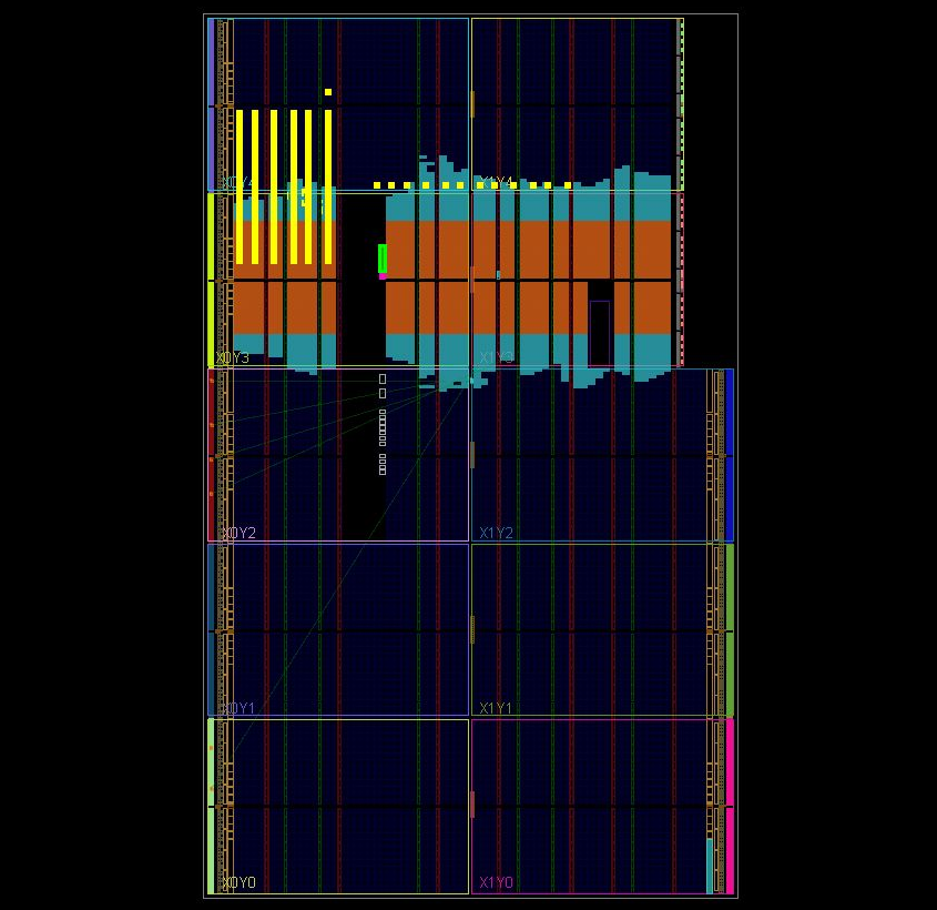
Pic.6
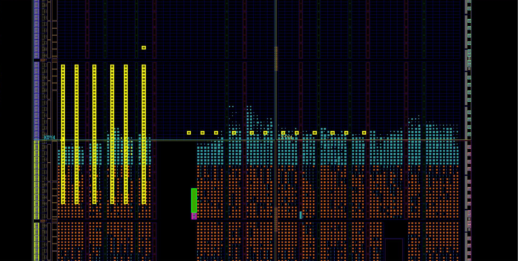
Fig.7
The test result can be viewed in the log files. The calculation of the faulty element looks like this: For example, the file: test_X0-108Y160-191_Dev1 (com5) .txt
ERROR AT A: 000D
WR: 55555555
RD: 43555555
Address 0xD, 13: Slice position: X = 13, Y = 160 + (wrong bit position) = 160 + 25 = 185 and the others: 186, 188. So, X = 13, Y = 185, 186,188
So positions of faulty slices were received. The test itself with the sources in the archive TEST_SLICES (27'07'2016) . In the Versions folder are bit files to run. They are designed for quartz 125 MHz, the port speed is 115200. In the pictures you can see a green rectangle, this is the XADC block, the one with the wrong power supply, 3.3 V instead of 1.8V. If XILINX is close to reality, it shows the location of the elements, then it can be seen that the assumption of crystal damage for this reason may be true. You can exclude the broken slices from the system and prohibit the breeder from using them with the commands:
set_property PROHIBIT 1 [get_sites SLICE_X17Y243] - prohibits individual slices.
set_property PROHIBIT 1 [get_sites -range SLICE_X1Y176: SLICE_X25Y223]
- Prohibits a set of slices.
A complete set of such commands can be found in the file main1.xdc in the project archive BRAM_TEST .
6.2 BRAM
Using the data about the broken slices, a test was constructed using 98% of the blocks.
of memory. The test result in fig. eight.
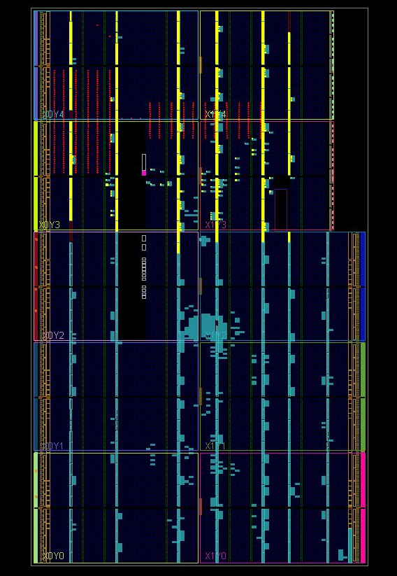
Fig.8
More detail in Figure 9. Red dots mark defective slices that are not used.
for test work.
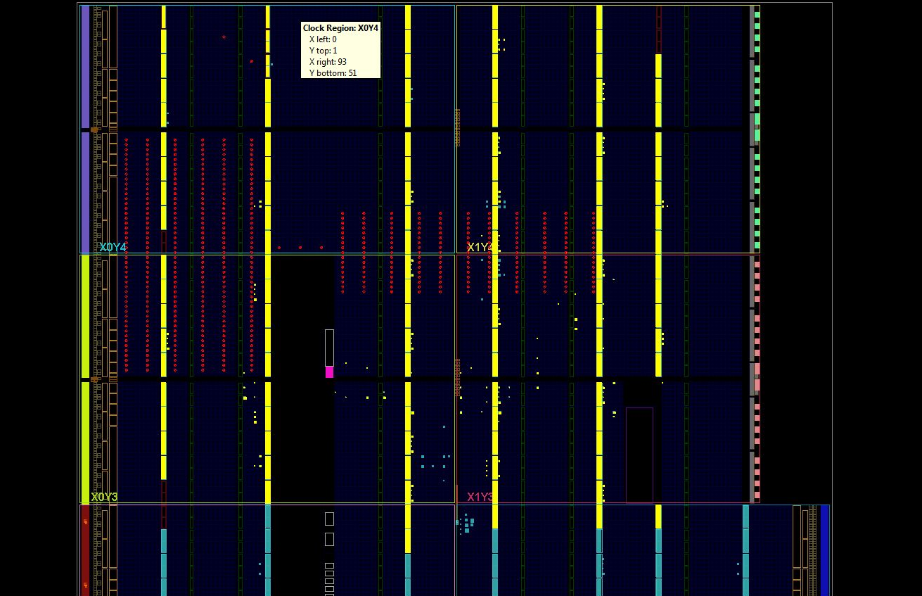
Fig.9
You can see that almost half of the BRAM memory is damaged. And the damaged area is so
However, it is closer to the ADC module, which is fed the wrong power. Perhaps it
not an accident. If we consider that the slice test does not show all the faults, but only by
One trigger and several LUTs per slice, I consider using a crystal with limiting
The number of cores for a project is not efficient. His work will be unpredictable, and may not
show reliable results. In addition, BRAM damage is too large. And also
it is necessary to take into account that some other chips may have other damages and not coincide with those already found.
Conclusion:
1. The board needs re-routing with power correction on ADC_VCC (M12) and installation
additional capacitors to the INHIBIT pins of stabilizers + 3.3V and + 1.8V. Also if
The RST signal is output out of the board with the help of long wires (not counting the board with
LEDs), it is desirable to provide protection against static electricity.
2. When there is a great need, you can try to build a project, for example, at 80-90
kernels, introducing restrictions on the use of BRAM and SLICES, without using an external RST pin, applying an internal generated reset.
PS: After following recommendation 1, the problems disappeared.
M. Ye. Generalov, 2018
Source: https://habr.com/ru/post/346622/
All Articles