NRF51822 in brief: Power saving and some peripherals

Good day.
In the last article, we briefly enough familiarized ourselves with the minimum set of BLE stack capabilities and created our first project for connecting two remote devices. Now it's time to pay attention to the nRF51822 hardware, namely to a 32-bit microcontroller based on the ARM architecture with the Cortex M0 core (256kB / 128kB flash + 32kB / 16kB RAM).
In this article, I would like to take the time to be probably one of the main features of Bluetooth Low Energy devices - energy saving, as well as consider the most frequently used peripherals, such as ADCs, timers, and interesting, I think PPI block. The remaining commonly used peripheral units such as SPI, I2C, UART will be considered in the following articles.
So, let's begin.
')
Power Saving Modes
As mentioned above, one of the key features of BLE chips is their low power consumption, which actually determines their use in various SMART devices. Let us consider what one of the leaders of the BLE segment offers - Nordic Semiconductor with its nRF51822.
According to the datasheet, nRF51822 has two main modes of operation, one of which is stationary with the possibility of switching sub-modes of energy saving, and one for achieving maximum energy savings.
System ON mode
System ON is the main mode in which the controller is fully functional and performs all the declared functions. The controller enters sleep mode using the WFI and WFE instructions, the difference between which is that in the first case, the awakening occurs by interrupting the allowed in NVIC, and in the second from any event that is allowed in NVIC and not allowed. System ON is notable for the fact that it can be in two states in sleep mode: Low power and Constant Latency.
Low power - low power mode, which is achieved by optimizing the power management system. In this case, part of the regulators is disabled (more details can be found in the product specification) and the crystal resonator, which leads to an increase in the time interval required for the core to wake up, as well as the delay in responding to the PPI module request (see below for the PPI module). this gap is not always constant and may vary depending on the periphery that caused the interruption. To enter Low Power you need to activate the task in the LOWPWR register. This mode is standard and it is the controller after Reset.
Constant Latency is a mode generally similar to the previous one, the only difference is that the delays of the kernel and the response to the PPI module request are constant and minimal. However, this entails a higher power consumption, since the quartz resonator remains on, although it is in the minimum consumption mode.
To enter Constant Latency, you must activate the task in the CONSTLAT register.
System ON consumption Low power directly depends on the number of active memory blocks and is:
2.6 µA - 16 Kb RAM Active
3.8 µA - 32 Kb RAM active
Experts and Nordic advise to adhere to a number of rules for a significantly greater reduction in energy consumption in System On mode:
- use built-in DC / DC (gain up to 30%);
- increase the interval between advertising packages;
- if possible, reduce the amount of advertising package;
- if possible, reduce the power of the radio transmitter;
- disable unused peripheral modules before switching to sleep mode;
- disable SPI, TWI, UART modules after the end of the receive / transmit cycle.
System OFF mode
System OFF - the mode in which the most economical power consumption mode is achieved. In this mode, the controller core is disabled and all processes are terminated. In this case, one or more RAM blocks remain active. Exit from this mode is possible by an external DETECT signal, by an ANADETECT signal from the built-in comparator LPCOMP, and also by a RESET signal. After exit, a forced system reset is performed.
To enter the System OFF mode, you must perform the following steps in the following registers:
1. RESETREAS - define a wake-up event in the register;
2. RAMON and RAMONB - determine the active RAM blocks in the register;
3. SYSTEMOFF - activate the System OFF mode in the register;
4. configure the unit responsible for waking the controller.
SystemOFF mode startup function
#define WAKEUP_PIN 1 void SystemOFF_active(void){ /* : */ NRF_POWER->RESETREAS = POWER_RESETREAS_OFF_Detected; /* RAM */ NRF_POWER->RAMON = POWER_RAMON_OFFRAM0_RAM0Off; /* P0.01 */ NRF_GPIO->PIN_CNF[WAKEUP_PIN] = (GPIO_PIN_CNF_DIR_Input << GPIO_PIN_CNF_DIR_Pos)| (GPIO_PIN_CNF_PULL_Pulldown << GPIO_PIN_CNF_PULL_Pos)| (GPIO_PIN_CNF_SENSE_High << GPIO_PIN_CNF_SENSE_Pos)| (GPIO_PIN_CNF_INPUT_Connect << GPIO_PIN_CNF_INPUT_Pos); /* P0.01*/ NRF_GPIOTE->CONFIG[0] = (GPIOTE_CONFIG_MODE_Event << GPIOTE_CONFIG_MODE_Pos)| (WAKEUP_PIN << GPIOTE_CONFIG_PSEL_Pos)| (GPIOTE_CONFIG_POLARITY_LoToHi << GPIOTE_CONFIG_POLARITY_Pos); /* SystemOFF*/ NRF_POWER->SYSTEMOFF = 1; } Consumption in this mode directly depends on the number of active memory blocks and is:
0.6 µA - no active RAM blocks
1.8 µA - 16 Kb RAM Active
3.0 µA - 32 KB RAM active
In general, an interesting energy saving mode, but not everyone will like it because of the meager list of possibilities to wake up the controller.
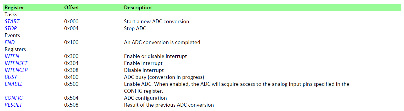
A / D Converter (ADC)
Analog-to-digital converter (ADC) is one of the most frequently used elements of the periphery of a microcontroller. I see no point in describing the principle of his work, since a great number of third-party articles of varying degrees of depth have been written about this. However, pay attention to the features of the ADC is worth. The nRF51822 has one ADC and its characteristics are quite modest:
- 8 channels + 2 external channels for supplying an external reference voltage;
- resolution of 8.9.10 bits;
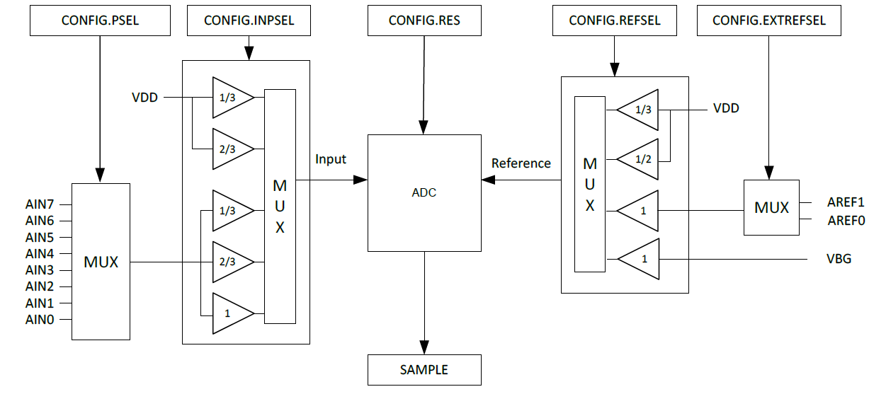
Actually, everything that can be said about the main characteristics. It should be noted that the channels are multiplexed, i.e. Sampling at a time can only occur from one channel, and the conversion mode, unfortunately, is only one - a one-time conversion. You can implement uninterrupted using a timer and a PPI module, but we'll talk about this a little later.
Also, an important parameter is the time of one conversion, which must be considered in the case of the implementation of continuous conversion of several channels with intermediate data processing.
68 μs - 10 bit ADC;
36 µs - 9 bit ADC;
20 μs - 9 bit ADC.
To activate the ADC in the single conversion mode, you must perform the following steps in the following registers:
1. CONFIG - determine the ADC digit capacity in the register;
2. CONFIG - determine the voltage divider in the register;
3. CONFIG — determine the channel number to be converted in the register;
4. POWER - activate interrupts (optional) in the register;
5. ENABLE - apply power to the ADC in the register.
6. TASKS_START - start the conversion in the register.
Below is an example of the initialization of the ADC for carrying out a single conversion with the subsequent processing of the result obtained in the interrupt.
ADC initialization function
/* */ /* - 10 , - 1/3, - 2 */ NRF_ADC->CONFIG |= (ADC_CONFIG_RES_10bit << ADC_CONFIG_RES_Pos)| (ADC_CONFIG_INPSEL_AnalogInputOneThirdPrescaling << ADC_CONFIG_INPSEL_Pos)| (ADC_CONFIG_PSEL_AnalogInput2 << ADC_CONFIG_PSEL_Pos); /* */ NRF_ADC->INTENSET |= ADC_INTENSET_END_Enabled << ADC_INTENSET_END_Pos; /* */ NRF_ADC->ENABLE |= ADC_ENABLE_ENABLE_Enabled << ADC_ENABLE_ENABLE_Pos; /* NVIC */ NVIC_SetPriority(ADC_IRQn, 1); NVIC_EnableIRQ(ADC_IRQn); /* */ NRF_ADC->TASKS_START = 1; ADC interrupt handler
/* */ #define ADC_REF 1200 #define ADC_PRESCALING 3 uint16_t adc_value, adc_value_in_mV; void ADC_IRQHandler(void){ /* , */ NRF_ADC->EVENTS_END = 0; /* */ switch(NRF_ADC->CONFIG >> ADC_CONFIG_PSEL_Pos){ case (ADC_CONFIG_PSEL_AnalogInput2): adc_value = NRF_ADC->RESULT; adc_value_in_mV = ((adc_value*ADC_REF)/1024)*ADC_PRESCALING break; /* */ default: break; } } I don’t see a more detailed description, as for people who read datasheets, the setting will not be difficult (there are few registers, all are intuitive), and for those who don’t like to read them, this information (and the one described below) will be enough to run and use the ADC.
Timers (TIMER)
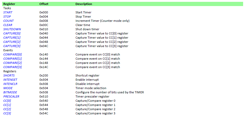
The nRF51822 has 3 timers that can operate in two modes: in timer mode (comparison) and counter (capture). All timers are 8, 16, 24 and 32 bit.
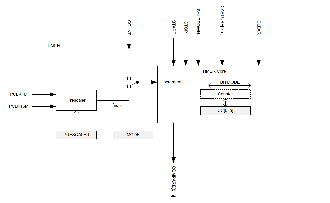
Timer mode (comparison): The most common timer mode. The current value of the counter is compared with the value in the CC [n] register and generates an event / interrupt when these two values match. The most commonly used mode, as with it you can count down time intervals.
Counter mode (signal capture): When an external pulse arrives, the timer captures (captures) the current counter value in the CC [n] register. At the next pulse, the timer again fixes the value of the counter in the same register. Thus, we can get the period or the duration of the input pulse. You can catch both the front of the pulse and the decline. Very useful timer operation mode.
The timer frequency is calculated using the following formula:
To activate the timer in compare mode, you must perform the following steps in the following registers:
1. MODE - determine the mode of the timer in the register;
2. PRESCALER - define the clock divider in the register;
3. CC [n] - determine the number of "ticks", up to which it is necessary to count in the register;
4. POWER - activate the power of the timer in the register;
5. TASKS_START - start the timer in the register.
Consider the initialization of the timer to count the time with an interval of 1 second. Below is the timer initialization function, as well as the timer interrupt handler function, when the value set in the CC [n] register is reached:
Timer initialization function
NRF_TIMER1->POWER = 1; /* */ NRF_TIMER1->MODE = TIMER_MODE_MODE_Timer << TIMER_MODE_MODE_Pos; /* . : (16 MHz) 2 9 31250 "" */ NRF_TIMER1->PRESCALER = 9; NRF_TIMER1->CC[0] = 31250; /* */ NRF_TIMER1->INTENSET = (TIMER_INTENSET_COMPARE0_Enabled << TIMER_INTENSET_COMPARE0_Pos); /* NVIC */ NVIC_SetPriority(TIMER1_IRQn, NRF_APP_PRIORITY_HIGH); NVIC_EnableIRQ(TIMER1_IRQn); /* */ NRF_TIMER1->TASKS_START = 1; Timer interrupt handler function
void TIMER1_IRQHandler(void){ /* , */ NRF_TIMER1->EVENTS_COMPARE[0] = 0; /* */ NRF_ADC->TASKS_CLEAR = 1; } Yes, there are 4 registers for storing the Capture / Compare value of 4 CC [0] - CC [3] , but the counting register is one, so only 4 consecutive results can be counted, then clear the counting register and start counting again.
PPI module
Now we slowly approached why I so briefly and incompletely described the capabilities of the timer and ADC, because it was possible, as in most similar articles for other controllers (for example, STM32), to allocate a separate post for each module, to discuss each register, every bit ... And all this is boring and secondary, any of the articles about ADCs or timers will give you the necessary minimum knowledge base and there is no point in producing it again and again. I propose to consider an interesting nRF51 module and with its help implement the standard TIMER + ADC bundle, thereby ensuring a continuous conversion mode with a given sampling rate.

What is the need for a PPI module?
A PPI module is needed to transfer event / interrupt data from one periphery to another without the involvement of the controller core. For example, an RTC (Real Time Counter) interrupt can run any peripheral unit without a CPU. In addition, communication via the PPI module between peripheral devices can occur when the CPU is sleeping or turned off.
In our case, this module can be used to start ADC conversion, as a consequence of the event when the timer reaches the set value. Thus, without the participation of the CPU, we will achieve the realization of a continuous conversion of the ADC.
So, the PPI module has 16 channels available for programming grouped into 4 groups. In addition, there are 12 channels already programmed by the system. Below is the setup of these 12 channels ( EEP is the address of the periphery that triggered the event, TEP is the address of the task to be performed in the event of an event).
As mentioned earlier, the module for each channel has two registers - the event register and the task register executed in the event of an event.
To activate the PPI module, you must perform the following steps in the following registers:
1. CHENSET - activate the module required channel in the register;
2. CH [n] .EPP - determine the address of the event in the register;
3. CH [n] .TEP - determine the address of the task in the register;
4. CHG [n] .EN - activate the group in which the given channel is in the register.
Below is the initialization function of the PPI module for the TIMER + ADC bundle.
Timer initialization function
/* . NRF_TIMER1->EVENTS_COMPARE[0] */ NRF_PPI->CH[0].EEP = 0x40009140; /* . NRF_ADC->TASKS_START */ NRF_PPI->CH[0].TEP = 0x40007000; /* */ NRF_PPI->CHEN |= PPI_CHEN_CH0_Enabled; NRF_PPI->CHENSET |= PPI_CHENSET_CH0_Enabled; /* PPI */ NRF_PPI->TASKS_CHG[0].EN = 1; A link to the project code of the TIMER + PPI + ADC bundle is in the appendix to the article.
I would like to draw your attention to the fact that as people correctly suggested in the comments to the previous article, the nRF51822 is not the most stable chip. There are a number of unobvious problems. In addition, the chip itself, on the one hand, is rich on the periphery, on the other hand, it is rather poor. The ADC is too slow, the lack of DMA for the part of the periphery for which it is most needed (SPIM, TWI, UART, ADC), the absence of FPU, all this limits this chip to use. Many will say that this is nonsense, since with leaner characteristics you can make a lot of cool devices, as long as your hands are from that place. And, in principle, they will be right. BUT, at the moment there is a debugging board nRF52 with a chip nRF52832, devoid of all the listed disadvantages and much more stable than the 51st series, with the same price tag. So be careful when choosing a controller for various tasks.
In the next article, if it is, I will talk about the features of the implementation of various interfaces (SPIS, SPIM, TWI, UART), can capture the RTC and other peripherals.
Additional Information
Timer + PPI + ADC bundle implementation project
PPI interface
NRF51822 in brief: Quick start
Source: https://habr.com/ru/post/345396/
All Articles