HyperRAM: Using a HyperBus Memory Interface Chip

We continue to acquaint Habr's readers with "non-standard" types of memory for electronics development. Last time we talked about the hybrid memory cube (HMC) and its connection to the FPGA, and in this article we will focus on memory chips with a Cypress HyperBus interface, which appeared on the market relatively recently, in 2014.
Two types of devices are now available: HyperRAM and HyperFLASH. HyperRAM is pseudo-static memory (DRAM + recharge circuit in one chip), and HyperFLASH is NOR flash memory with a HyperBUS interface. Combined 2 in 1 chips are also available: HyperFLASH 512Mb + HyperRAM 64Mb. The value of modern solutions lies in a small number of signals, a small footprint, a fairly high speed of work and an adequate price.
For example, this is how Cypress (the main promoter of HyperBUS) sees the next generation of these memory chips in automotive electronics headed by its controller:

')
That is, Cypress offers to replace all external memory with a single chip. In general, this proposal is not unreasonable, especially for projects with strict requirements for the size of the boards.
Despite a number of advantages compared to SRAM, DRAM and conventional FLASH, the widespread adoption of HyperBUS solutions has not yet happened, since more recently - last year - such devices were supported by only one microcontroller from Cypress (and FPGA, of course). Now business moves forward and more and more microcontrollers provide its support.
Two weeks ago, on December 5, 2017, Cypress announced the inclusion of the HyperBus memory interface in the xSPI (eXpanded SPI) standard, which is coordinated by JEDEC, the semiconductor products engineering standardization committee. The xSPI standard defines the compatibility requirements for high-performance serial interfaces so that manufacturers of controllers and chipsets can develop a universal memory controller. The inclusion of the HyperBus interface in the JEDEC xSPI standard should simplify HyperBus-based memory design and provide greater flexibility in implementing insant on when developing electronics for cars, industrial automation and the Internet of things (IoT).
HyperBus memory interface microcircuits are very promising, and we are in a hurry to share the experience of using them in one of our projects.
Task Description
Before proceeding to the story about the interface, we will explain in which problem it was applied. In the next development, we had to provide data output to an external device with minimal latency and a sufficiently large bandwidth. At the same time, there is not much space on the board, it is not at all. On a shawl the size of a matchbox, it was necessary to fit a processor with Linux on board, plus an appropriate binding, a USB controller, an FPGA that actually accesses the memory and gives the data out, and some other specific stuffing. Naturally, all components were subject to rigorous selection.
As a result, the choice of memory chips fell on HyperRAM. Parameters: the number of signals to connect to the FPGA - 12; maximum latency - 36 ns; bandwidth - 333 MB / s; volume - 8 MB; body - 6x8x1.2 mm TF-BGA.
For comparison: SRAM of a similar volume will require 35 lines, and SDRAM - and even more. At the same time, SRAM will cost an order of magnitude more than HyperRAM, and SDRAM will require titanic tracer effort and lead to a significant increase in the cost of the printed circuit board.
The requirement to minimize latency did not allow the use of third-party high-level IP modules (such as AVALON <-> HyperBus with pipelining and scheduling). As a result, our task was to develop a specialized IP module for working with HyperRAM.
The module was developed on the HyperMAX debug board from devboards. The board contains two interesting devices: HyperRAM and HyperFLASH from ISSI. In addition, the board is crammed with different buns, focused on the use in automotive electronics.

It is worth noting that IP modules available on the market support working with HyperBUS via AXI4 and AVALON interfaces, and also declare the possibility of executing software programs from the software processors directly from HyperFLASH [ for example ].
A few words about debugging HyperMAX (revision 1.1)
Examples of projects are very mediocre. A project for HyperRAM in general with an incomprehensible logic of choosing the operating frequency. Instead of registering the constraints on the RWDS, a fixed signal delay is set in the input buffer, and HyperRAM works in a shamanic manner at 116 MHz. DDR signals are input to the input pins with SDR buffers. It is impossible to screw the nut on the rack, because the hole is placed close to the connector. At one of the connectors on the pin, a GPIO-signal is output according to the scheme, but in fact it is not there. And this we have not checked everything. In general, despite the fact that the Germans developed the HyperMAX board and it costs ~ 300 euros, the debugging is damp. But, as they say, "with all the wealth of choice, there is no other alternative."
Next, we describe the work with the HyperRAM chip. Interaction with HyperFLASH is organized in a similar way, but with some simplifications.
HyperRAM Memory
The HyperRAM chip is a high-speed DRAM-CMOS memory that works on the HyperBUS interface with a built-in recharge mechanism. The recharge circuit works when no read / write operations are in progress. As a result, from the point of view of the host, the memory looks static and is called pseudo-static memory (PSRAM).
HyperBus is a DDR interface that allows you to achieve high read / write speeds when using a small number of signals. Data is transmitted over an 8-bit bus in 16-bit words per clock cycle. All lines are LV-CMOS compatible. The devices are available in two versions of the supply voltage: 1.8 V and 3.0 V.
According to the specification, the HyperBUS interface contains mandatory and optional signals.
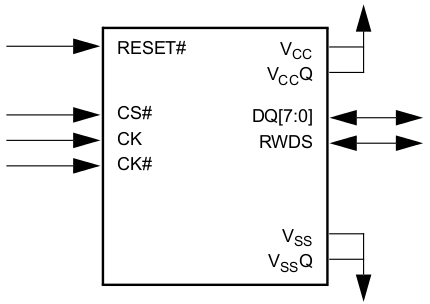
Key HyperBUS Interface Signals
In our case, only mandatory ones were used (see figure above):
- CS # - device selection signal. The presence of a chip select signal allows you to combine several devices with one bus with the master slave architecture.
- CK / CK # - clock signal. Devices powered by 3 V are synchronized over one CK line at frequencies not exceeding 100 MHz, and with 1.8 V power supply - with a differential CK / CK # pair at frequencies up to 166 MHz.
- DQ [7: 0] is a bidirectional data bus.
- RWDS is a multifunctional bidirectional signal ( R ead W rite D ata S trobe).
The RWDS signal performs the following functions:
- At the beginning of a transaction, it is driven by memory and indicates the required latency before issuing / writing data: 0 - one time delay; 1 - double delay (initial read / write latency).
- In write transactions in the process of issuing data is driven by the host and masks the bytes that should not be changed.
- In read transactions in the process of issuing data, it is driven by memory and synchronized data (source syncronous read data strobe).
About latency and synchronization will be discussed below.
Data exchange with the device takes place in the form of transactions: the master will arrange the chip-select, provides a clock signal, issues control bytes, waits for several cycles, communicates, stops synchronization, and de-selects the chip-select.
In the first three cycles, the host transmits 6 transaction control bytes (COMMAND-ADRESS or CA ). Without going into details, simply list the parameters:
- Transaction type: read or write.
- Address space: memory or control registers.
- The type of write / read sequence: linear (linear) or batch (burst).
- The address for starting memory access in columns and rows.
Since memory cells cannot be recharged during a data exchange transaction, restrictions are imposed on the duration of a single transaction (transaction duration) and the delay between them (initial latency).
Simultaneously with the transfer of the CA, the memory puts on the RWDS line an indicator of latency: how many clock cycles must be waited before issuing data for writing, or receiving data for reading. The value of the number of cycles we learn from the control register. This value is determined by the memory independently, depending on the clocking frequency. If RWDS is at “0”, we expect the required number of cycles once, if at “1” - twice. By setting the device registers, you can set the memory to always work on a double delay interval, and set the number of ticks different from the default value (but this value should not be less than the original).
In a write transaction, after waiting for the required number of ticks, the host puts write data to the bus:

Write transaction
The data is captured by the memory on both fronts of the sync signal, respectively, the data are set in the output DDR register by a clock shifted 270 degrees. The RWDS signal in the data transfer process masks the bytes that should not be changed by the memory in the recording process. When writing a word to the control registers, it must be issued immediately after the SA without any delay.
In a read transaction, the data is set in memory:

Read transaction
Data changes on the bus are synchronized with both edges of the RWDS signal. You should also not forget that the data generated by the memory is synchronized by the RWDS signal on the front. As a result, for correct reading, RWDS should be shifted by 90 degrees:

RWDS signal delay relative to data signal
Data reading / reading begins at the address specified in the CA. The address with each received / issued word is incremented by 2. The transaction ends when the clock signal stops and the chipset deassert stops.
We note several features of the work. First, when the address goes over the maximum value, data starts to be output / recorded in an indefinite manner. Therefore, you should not access the memory of transactions that overflow the address counter. Second, the microcircuit limits the duration of the transaction, since periodic recharging of the memory elements is required. Maximum durations depend on temperature and are given in the specification. In the toughest case, in one transaction at a speed of 166 MHz, you can read / write a little more than 300 bytes.
The device has two registers: information and configuration. The information register provides us with information about the manufacturer and type of device (HyperRAM / HyperFLASH), the number of rows, columns and crystals of the device. The configuration register allows configuring the output impedance, packet length in the packet data access mode, latency type (constant / variable), and also allows you to set the delay value and put the device into low power consumption mode (Deep Power Down).
At first glance, the question may arise: how do I read the value of the configuration register with information about the delay, if this delay is unknown at the time of reading? For this it is necessary to take into account that the data output is synchronized by the memory along the RWDS line. And, in fact, the actual value of the delay is not taken into account anywhere, since the data capture scheme is source-synchronous. And in the transaction record, on the contrary, we must count the cycles before issuing data, depending on the value of latency and the state of the RWDS signal.
Here is an example of parsing the values of the configuration registers:

findings
In general, the memory interface HyperBUS left only pleasant impressions. On the FPGA, working with it is fairly simple and the developed module is not at all resource-intensive. The only current drawback is the limited range of microcontrollers with HyperBUS. So we will wait for the interface support by a large number of vendors and uniquely implement it in our (and in your :-) future projects.
Source: https://habr.com/ru/post/344966/
All Articles