The evolution of solid-state drives: from the first models of the 70s to the present day
In October 2016, we introduced two lines of 2.5-inch solid-state drives: the WD Blue and Green SSD. In any other industry, such a move could seem quite risky even for a corporation such as Western Digital. Indeed, the promotion of new products in the niche, where spheres of influence have long been defined, in most cases turns into large financial costs and rarely leads to positive results. However, the SSD market has its own specifics, opening up tremendous opportunities for competition, which is due to both technological features and a number of historical prerequisites. It is about the history of the emergence of solid-state drives, and we'll talk today.
Strictly speaking, SSD appeared long before the invention of flash memory. After all, what is, in fact, Solid State Drive? This is an information storage device that does not contain any mechanical components. Thus, the very first SSD in the world can be called the creation of the corporation Dataram with the proud name Bulk Core, presented in 1976. Steel chassis dimensions of 19 by 15.75 inches contained 8 strips of volatile RAM-memory, each of which had a volume of 256 kilobytes. A device the size of a good UPS (and, due to the presence of backup batteries, an appropriate weight) cost from the start $ 9,700. The devices have found application in industry and knowledge-intensive industries, however, due to the high cost and unreliability (the risk of data loss was still extremely high), they did not become widespread.

Dataram Bulk Core - the very first SSD
')
However, after only 6 years, Axlon attempted to conquer the consumer segment by entering the market with an external RAM Disk, designed specifically for the Apple II personal computers released in 1982. The novelty carried onboard 320 kilobytes of RAM, had dimensions comparable to modern compact NAS and was equipped with rechargeable batteries, providing 3 hours of autonomous work in case of power outages.

The Axlon RAM Disk brochure encourages your Apple II to bleed.
You can guess how popular this solution was by looking at the prices: at the start of sales, the device cost $ 1,400, while the Apple II itself in a modification with 4 kilobytes of RAM at that time would have cost you $ 1,298. Let the built-in permanent memory this PC also had 4 kilobytes, the ability to connect a cassette recorder, and subsequently 5.25-inch drives more than compensated for this shortcoming. At the same time, the exorbitant price tag and the risk of losing all information made the RAM Disk unattractive for the end user, especially since most users simply didn’t need additional read / write speed.
All of the above devices were unprofitable due to the high cost, unreliable due to the need for a constant power source and unnecessarily cumbersome due to design features. In other words, solid state drives of the past were deprived of all the advantages of modern models, which explains their fiasco. To create a truly revolutionary solution, a fundamentally new technology was needed, which appeared only in the mid-80s with the invention of flash memory.
Semiconductor memory devices existed before: the first EPROM was created by Dov Froman in 1971, but such chips were not suitable for the role of even a removable drive. The fact is that the procedure of erasing information was carried out by direct irradiation of the matrix of transistors with an ultraviolet mercury lamp, for which the case even had a small window made of quartz glass, located directly above the chip. More advanced EEPROMs were already electrically erasable ROMs; however, to realize this possibility, a second transistor controlling recording and erasing modes had to be introduced into a standard cell. Because of this, the layout area of the matrix components (and, therefore, the chip itself) increased markedly, and as a result, we had to sacrifice the compactness of the devices.
Therefore, the main scientific research was conducted in the field of chip design with a more dense arrangement of erase chains. And they were crowned with success in 1984, when Fujio Masuoka, who worked at Toshiba, presented a prototype of non-volatile flash memory at the International Electron Devices Meeting conference held at the Institute of Electrical and Electronics Engineers (IEEE).

Fujio Masuoka, inventor of flash memory
The name itself was invented by his colleague, Shoji Ariidzumi, who compared the process of erasing data with a flash of lightning. Unlike the EEPROM, the flash memory was based on MOS transistors with an additional floating gate located between the p-layer and the control gate, which made it possible to create truly miniature chips.
Intel's NOR (Not-Or) technology chips, which were launched in 1988, became the first commercial flash memory samples. The matrices of this type were a two-dimensional array in which each memory cell was at the intersection of a row and a column (the corresponding conductors were connected to different gates of the transistor, and the source was connected to a common substrate). However, in 1989, Toshiba introduced the NAND flash memory. The array had a similar structure, but in each of its nodes, instead of a single cell, there were now several series-connected ones. In addition, two MOS transistors were used in each line — a control, located between the bit line and a column of cells, and a grounding transistor.
The higher density of the layout helped to increase the capacity of the chip, but at the same time the read / write algorithm became more complicated, which caused the speed of information exchange. In this regard, the new architecture could not completely supplant the NOR, which has found application in the creation of embedded ROMs, whereas NAND was used in the manufacture of portable drives (USB flash drives, SD cards). By the way, the production of the latter became possible only in 2000, when the cost of flash memory was sufficiently reduced and such devices could pay off, and the first “swallow” was IBM's DiskOneKey model, which was only 8 megabytes. Not much, but let's not forget that a miniature device the size of a keychain successfully replaced eight 3.5-inch floppy disks.

Flash drive IBM DiskOneKey
Since the release of flash chips is a technologically complex and knowledge-intensive process, there are only a few companies specializing in their production, among which should be highlighted SanDisk. She has more than 200 patents, licenses for the use of which were later acquired by such well-known players like Intel, Hitachi, Samsung and Sony. Among the main achievements of the company, the introduction of the CompactFlash standard (1994), the development of the MultiMedia Card (1997) and the Secure Digital Memory Card (SD) format created with Toshiba in 2000 are worth mentioning. Not surprisingly, when Toshiba headed for the US market, it was SanDisk that was chosen as the strategic partner for founding the joint venture FlashVision LLC (launched in 2001) based on the production capacity of the subsidiary of the Japanese giant Dominion Semiconductor. In October 2015, SanDisk was acquired by Western Digital. By joining forces with one of the pioneers of Flash technology and gaining access to all key developments and innovations, today we have the opportunity to create truly modern, competitive and reliable consumer-class solutions.
However, back to the subject of discussion - SSD. The ancestor of modern solid-state drives based on flash memory was released by Digipro in 1988: it carried 16 megabytes on board and cost $ 5,000. A year later, M-Systems introduced the concept of the device, more or less resembling modern ones. It had a format of 3.5 inches and could hold from 16 to 896 megabytes of information. The serial model was released only in 1995 and was called FFD-350 (Fast Flash Disk). Because of the high price, reaching several tens of thousands of dollars, it found application in industries such as the military-industrial complex and the aviation industry, for the retail record-breaker in speed and volume was unsuitable.
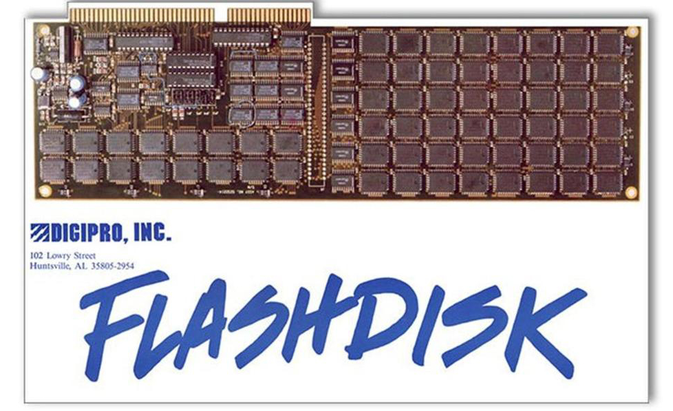
Digipro Flashdisk - the first NAND based SSD
The pioneer of the consumer segment can be called the Transcend IDE Flash Module, released in 2003, which connected via the 44-pin Parallel ATA interface and had a volume of 128 or 512 megabytes. The product was positioned as a fast and failsafe drive for working in extreme conditions. The low-profile module was only 2 centimeters above the connector, so it could be connected directly without using a loop.
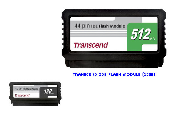
Transcend IDE Flash Module opens up the retail SSD market
And the first SATA SSD appeared just a year later: Adtron Corporation introduced the 2.5-inch Flashpack drive, but its market value, depending on the modification, reached $ 11,200. Samsung managed to change the situation in terms of pricing policy, offering buyers a device with a simple name Flash SSD with a capacity of 32 gigabytes "for only 700 dollars"! And let it still be difficult to call it truly massive, enthusiasts who are ready to fork out for the performance gain of the top PC, this option came to taste.
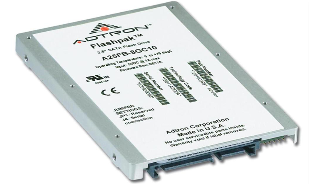
Adtron Flashpack - the prototype of modern SSD
Reducing the cost and increasing the attractiveness of SSD for the average consumer is largely made possible by the emergence of multi-bit memory cells. Initially, the architecture of flash matrices assumed the possibility of recording only one bit of information in each cell, that is, a floating gate could store only two charge levels (this type of memory was called SLC - Single-Level Cell). The next step was the creation of an MLC (Multi-Level Cell) capable of storing 2 bits (four charge levels) per cell. The 8-level (3 bits) TLC flash memory (triple-level cell), also called the 3bit MLC, turned out to be even more capacious and cheaper in production. As of 2015, its cost fell to 40 cents per gigabyte.
Like NOR and NAND, each of these solutions has its own niche. After all, if SLC provides the maximum speed of access to the stored information and is extremely fault tolerant, then TLC is characterized by budget and a higher storage density. In the cons of the latter, you can write a much smaller working resource. As a result, SLC has become widespread in the corporate segment, TLC has become an absolute monopolist in retail, and products based on MLC are focused primarily on those who value reliability and want to squeeze everything out of their car.
Further development of the SSD was carried out by improving the interfaces of the microcircuits. At the time when there was a question about the introduction of uniform standards, a consortium of technology companies that included Intel, Sony, SanDisk, Micron Technology, Numonyx, Phison Electronics Corporation, SK Hynix, Spansion and STMicroelectronics developed the Open NAND Flash Interface Specification (ONFI), the first version which was presented in spring 2006. The capacity of ONFI 1.0 was only 50 MB / s and was unable to unleash the full potential of even SATA II - only its 4th revision, released in 2014, was able to step over the bar set by SATA III, demonstrating a data transfer rate of 800 MB / with and providing a noticeable performance boost.
An equally important role was played by the improvement of read / write algorithms and caching. For example, creating WD Blue SSD drives, we focused on improving performance by implementing nCache 2.0 technology, which uses part of the available memory in SLC mode and forces random read to be used in real-world load scenarios.

WD Blue SSD 1 TB - the flagship of the line of the first generation of solid-state drives from Western Digital
Direct copying of data from the SLC buffer to TLC, implemented at the chip level bypassing the controller, made it possible to use the more economical four-channel Marvell 88SS1074 model without any loss in performance. By the way, the latter supports error correction based on LDPC codes, due to which the WD Blue SSD can boast a rewriting resource of up to 400 TBW, which is more than 50% higher compared to other solutions in this price category. Thus, having introduced the listed innovations, we managed to create a truly competitive product based on TLC-memory, combining high speed and reliability at a relatively low price.
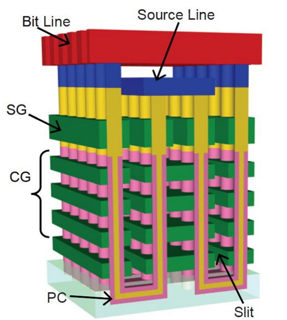
While all of the above has improved the performance and fault tolerance of drives, the potential of a two-dimensional NAND has been limited. When the capabilities of the 15-nanometer process technology were almost exhausted, and further improvement of the software part ceased to provide any noticeable increase in key indicators, the 3D NAND flash memory came to replace the planar chips. Its architecture is characterized by a vertical layout: conductive and insulating layers are sprayed onto the crystal in layers. In the resulting “puff” channels are formed, on the walls of which the structures of insulators and floating gates are applied - as a result, we get columns of ring-shaped field-effect transistors. This approach allows to significantly increase the density of chips, and thus increase the memory capacity.

3D NAND Layout
In itself, the invention can not be called know-how - for example, Samsung has been producing three-dimensional chips since 2013. But, as you know, the story moves in a spiral: just as flash drives appeared ten years after the creation of NAND because of the high cost of the latter, the first 3D chips turned out to be too expensive and, therefore, unsuitable for the consumer market. That is why the main efforts of the Toshiba and SanDisk alliance, which was already a division of Western Digital at that time, were aimed at developing a fundamentally different approach that would optimize production, making the chips more accessible.
Researches were crowned with success - the result of the painstaking work of engineers was the emergence of BiCS (Bit Cost Scalable) 3D NAND. Compared with the solution from Samsung, which supports only 48 layers in each chip, the BiCS technology allows to increase the packing density by 1.4 times and increase the number of layers to 64. The architecture has also undergone changes: U-shaped lines took the place of linear lines. Their main feature is that the source lines along with switching transistors are located in the upper part of the crystal, which almost completely eliminates the appearance of errors during read / write operations due to high temperature exposure.
BiCS Architecture
What does this mean in practice? Since BiCS 3D NAND is created on 40-nm process technology, and the need for the use of photolithography in the deep ultraviolet is completely absent, there is no need to upgrade the existing production facilities. Given the higher density of data storage, the cost of production in comparison with planar chips practically does not change, allowing you to create high-capacity drives. In addition, the new design improves the energy efficiency of chips by 25% and increases their reliability by eliminating the likelihood of thermal damage.
All of the above made it possible to create next-generation WD SSD Blue solid-state drives based on 64-layer chips. Compared to its predecessors, the disks are characterized by high speed (read speed reaches 560 MB / s, recording - 540 MB / s), MTBF up to 1.75 million hours and rewriting resource up to 500 TBW. In other words, even with a load of up to 80 gigabytes per day, the drives will run for 7 years, which is an absolute record in the average price category. In addition, due to the increase in recording density, the updated lineup has been supplemented with a two-byte flagship - an impressive amount and excellent performance make this model an ideal solution for professionals and enthusiasts.
Already, it can be argued that the cheapening of 3D NAND will make its use ubiquitous. A further arms race will shift towards an increase in the density of three-dimensional crystals and the development of original architectural solutions, which will make it possible to create truly affordable and economical products. It is possible that in such segments as the production of laptops, classic HDDs will be completely squeezed out of the market by solid state drives. The trend is already visible: according to DRAMeXchange forecasts (a division of TrendForce analytical agency), this year the share of laptops equipped exclusively with SSD will exceed 56% of all devices sold, and in the future this figure will only increase. However, the development prospects of the industry is a topic for a separate material, which we will definitely prepare for Habr's readers. Stay tuned for blog updates!
Pioneers of SSD - fast, expensive, not for everyone
Strictly speaking, SSD appeared long before the invention of flash memory. After all, what is, in fact, Solid State Drive? This is an information storage device that does not contain any mechanical components. Thus, the very first SSD in the world can be called the creation of the corporation Dataram with the proud name Bulk Core, presented in 1976. Steel chassis dimensions of 19 by 15.75 inches contained 8 strips of volatile RAM-memory, each of which had a volume of 256 kilobytes. A device the size of a good UPS (and, due to the presence of backup batteries, an appropriate weight) cost from the start $ 9,700. The devices have found application in industry and knowledge-intensive industries, however, due to the high cost and unreliability (the risk of data loss was still extremely high), they did not become widespread.
Dataram Bulk Core - the very first SSD
')
However, after only 6 years, Axlon attempted to conquer the consumer segment by entering the market with an external RAM Disk, designed specifically for the Apple II personal computers released in 1982. The novelty carried onboard 320 kilobytes of RAM, had dimensions comparable to modern compact NAS and was equipped with rechargeable batteries, providing 3 hours of autonomous work in case of power outages.
The Axlon RAM Disk brochure encourages your Apple II to bleed.
You can guess how popular this solution was by looking at the prices: at the start of sales, the device cost $ 1,400, while the Apple II itself in a modification with 4 kilobytes of RAM at that time would have cost you $ 1,298. Let the built-in permanent memory this PC also had 4 kilobytes, the ability to connect a cassette recorder, and subsequently 5.25-inch drives more than compensated for this shortcoming. At the same time, the exorbitant price tag and the risk of losing all information made the RAM Disk unattractive for the end user, especially since most users simply didn’t need additional read / write speed.
The invention of flash memory is a new era in the development of SSD
All of the above devices were unprofitable due to the high cost, unreliable due to the need for a constant power source and unnecessarily cumbersome due to design features. In other words, solid state drives of the past were deprived of all the advantages of modern models, which explains their fiasco. To create a truly revolutionary solution, a fundamentally new technology was needed, which appeared only in the mid-80s with the invention of flash memory.
Semiconductor memory devices existed before: the first EPROM was created by Dov Froman in 1971, but such chips were not suitable for the role of even a removable drive. The fact is that the procedure of erasing information was carried out by direct irradiation of the matrix of transistors with an ultraviolet mercury lamp, for which the case even had a small window made of quartz glass, located directly above the chip. More advanced EEPROMs were already electrically erasable ROMs; however, to realize this possibility, a second transistor controlling recording and erasing modes had to be introduced into a standard cell. Because of this, the layout area of the matrix components (and, therefore, the chip itself) increased markedly, and as a result, we had to sacrifice the compactness of the devices.
Therefore, the main scientific research was conducted in the field of chip design with a more dense arrangement of erase chains. And they were crowned with success in 1984, when Fujio Masuoka, who worked at Toshiba, presented a prototype of non-volatile flash memory at the International Electron Devices Meeting conference held at the Institute of Electrical and Electronics Engineers (IEEE).
Fujio Masuoka, inventor of flash memory
The name itself was invented by his colleague, Shoji Ariidzumi, who compared the process of erasing data with a flash of lightning. Unlike the EEPROM, the flash memory was based on MOS transistors with an additional floating gate located between the p-layer and the control gate, which made it possible to create truly miniature chips.
Intel's NOR (Not-Or) technology chips, which were launched in 1988, became the first commercial flash memory samples. The matrices of this type were a two-dimensional array in which each memory cell was at the intersection of a row and a column (the corresponding conductors were connected to different gates of the transistor, and the source was connected to a common substrate). However, in 1989, Toshiba introduced the NAND flash memory. The array had a similar structure, but in each of its nodes, instead of a single cell, there were now several series-connected ones. In addition, two MOS transistors were used in each line — a control, located between the bit line and a column of cells, and a grounding transistor.
The higher density of the layout helped to increase the capacity of the chip, but at the same time the read / write algorithm became more complicated, which caused the speed of information exchange. In this regard, the new architecture could not completely supplant the NOR, which has found application in the creation of embedded ROMs, whereas NAND was used in the manufacture of portable drives (USB flash drives, SD cards). By the way, the production of the latter became possible only in 2000, when the cost of flash memory was sufficiently reduced and such devices could pay off, and the first “swallow” was IBM's DiskOneKey model, which was only 8 megabytes. Not much, but let's not forget that a miniature device the size of a keychain successfully replaced eight 3.5-inch floppy disks.
Flash drive IBM DiskOneKey
Since the release of flash chips is a technologically complex and knowledge-intensive process, there are only a few companies specializing in their production, among which should be highlighted SanDisk. She has more than 200 patents, licenses for the use of which were later acquired by such well-known players like Intel, Hitachi, Samsung and Sony. Among the main achievements of the company, the introduction of the CompactFlash standard (1994), the development of the MultiMedia Card (1997) and the Secure Digital Memory Card (SD) format created with Toshiba in 2000 are worth mentioning. Not surprisingly, when Toshiba headed for the US market, it was SanDisk that was chosen as the strategic partner for founding the joint venture FlashVision LLC (launched in 2001) based on the production capacity of the subsidiary of the Japanese giant Dominion Semiconductor. In October 2015, SanDisk was acquired by Western Digital. By joining forces with one of the pioneers of Flash technology and gaining access to all key developments and innovations, today we have the opportunity to create truly modern, competitive and reliable consumer-class solutions.
Flash SSD for everyone
However, back to the subject of discussion - SSD. The ancestor of modern solid-state drives based on flash memory was released by Digipro in 1988: it carried 16 megabytes on board and cost $ 5,000. A year later, M-Systems introduced the concept of the device, more or less resembling modern ones. It had a format of 3.5 inches and could hold from 16 to 896 megabytes of information. The serial model was released only in 1995 and was called FFD-350 (Fast Flash Disk). Because of the high price, reaching several tens of thousands of dollars, it found application in industries such as the military-industrial complex and the aviation industry, for the retail record-breaker in speed and volume was unsuitable.
Digipro Flashdisk - the first NAND based SSD
The pioneer of the consumer segment can be called the Transcend IDE Flash Module, released in 2003, which connected via the 44-pin Parallel ATA interface and had a volume of 128 or 512 megabytes. The product was positioned as a fast and failsafe drive for working in extreme conditions. The low-profile module was only 2 centimeters above the connector, so it could be connected directly without using a loop.
Transcend IDE Flash Module opens up the retail SSD market
And the first SATA SSD appeared just a year later: Adtron Corporation introduced the 2.5-inch Flashpack drive, but its market value, depending on the modification, reached $ 11,200. Samsung managed to change the situation in terms of pricing policy, offering buyers a device with a simple name Flash SSD with a capacity of 32 gigabytes "for only 700 dollars"! And let it still be difficult to call it truly massive, enthusiasts who are ready to fork out for the performance gain of the top PC, this option came to taste.
Adtron Flashpack - the prototype of modern SSD
Reducing the cost and increasing the attractiveness of SSD for the average consumer is largely made possible by the emergence of multi-bit memory cells. Initially, the architecture of flash matrices assumed the possibility of recording only one bit of information in each cell, that is, a floating gate could store only two charge levels (this type of memory was called SLC - Single-Level Cell). The next step was the creation of an MLC (Multi-Level Cell) capable of storing 2 bits (four charge levels) per cell. The 8-level (3 bits) TLC flash memory (triple-level cell), also called the 3bit MLC, turned out to be even more capacious and cheaper in production. As of 2015, its cost fell to 40 cents per gigabyte.
Like NOR and NAND, each of these solutions has its own niche. After all, if SLC provides the maximum speed of access to the stored information and is extremely fault tolerant, then TLC is characterized by budget and a higher storage density. In the cons of the latter, you can write a much smaller working resource. As a result, SLC has become widespread in the corporate segment, TLC has become an absolute monopolist in retail, and products based on MLC are focused primarily on those who value reliability and want to squeeze everything out of their car.
Further development of the SSD was carried out by improving the interfaces of the microcircuits. At the time when there was a question about the introduction of uniform standards, a consortium of technology companies that included Intel, Sony, SanDisk, Micron Technology, Numonyx, Phison Electronics Corporation, SK Hynix, Spansion and STMicroelectronics developed the Open NAND Flash Interface Specification (ONFI), the first version which was presented in spring 2006. The capacity of ONFI 1.0 was only 50 MB / s and was unable to unleash the full potential of even SATA II - only its 4th revision, released in 2014, was able to step over the bar set by SATA III, demonstrating a data transfer rate of 800 MB / with and providing a noticeable performance boost.
An equally important role was played by the improvement of read / write algorithms and caching. For example, creating WD Blue SSD drives, we focused on improving performance by implementing nCache 2.0 technology, which uses part of the available memory in SLC mode and forces random read to be used in real-world load scenarios.
WD Blue SSD 1 TB - the flagship of the line of the first generation of solid-state drives from Western Digital
Direct copying of data from the SLC buffer to TLC, implemented at the chip level bypassing the controller, made it possible to use the more economical four-channel Marvell 88SS1074 model without any loss in performance. By the way, the latter supports error correction based on LDPC codes, due to which the WD Blue SSD can boast a rewriting resource of up to 400 TBW, which is more than 50% higher compared to other solutions in this price category. Thus, having introduced the listed innovations, we managed to create a truly competitive product based on TLC-memory, combining high speed and reliability at a relatively low price.
While all of the above has improved the performance and fault tolerance of drives, the potential of a two-dimensional NAND has been limited. When the capabilities of the 15-nanometer process technology were almost exhausted, and further improvement of the software part ceased to provide any noticeable increase in key indicators, the 3D NAND flash memory came to replace the planar chips. Its architecture is characterized by a vertical layout: conductive and insulating layers are sprayed onto the crystal in layers. In the resulting “puff” channels are formed, on the walls of which the structures of insulators and floating gates are applied - as a result, we get columns of ring-shaped field-effect transistors. This approach allows to significantly increase the density of chips, and thus increase the memory capacity.
3D NAND Layout
In itself, the invention can not be called know-how - for example, Samsung has been producing three-dimensional chips since 2013. But, as you know, the story moves in a spiral: just as flash drives appeared ten years after the creation of NAND because of the high cost of the latter, the first 3D chips turned out to be too expensive and, therefore, unsuitable for the consumer market. That is why the main efforts of the Toshiba and SanDisk alliance, which was already a division of Western Digital at that time, were aimed at developing a fundamentally different approach that would optimize production, making the chips more accessible.
Researches were crowned with success - the result of the painstaking work of engineers was the emergence of BiCS (Bit Cost Scalable) 3D NAND. Compared with the solution from Samsung, which supports only 48 layers in each chip, the BiCS technology allows to increase the packing density by 1.4 times and increase the number of layers to 64. The architecture has also undergone changes: U-shaped lines took the place of linear lines. Their main feature is that the source lines along with switching transistors are located in the upper part of the crystal, which almost completely eliminates the appearance of errors during read / write operations due to high temperature exposure.
BiCS Architecture
What does this mean in practice? Since BiCS 3D NAND is created on 40-nm process technology, and the need for the use of photolithography in the deep ultraviolet is completely absent, there is no need to upgrade the existing production facilities. Given the higher density of data storage, the cost of production in comparison with planar chips practically does not change, allowing you to create high-capacity drives. In addition, the new design improves the energy efficiency of chips by 25% and increases their reliability by eliminating the likelihood of thermal damage.
All of the above made it possible to create next-generation WD SSD Blue solid-state drives based on 64-layer chips. Compared to its predecessors, the disks are characterized by high speed (read speed reaches 560 MB / s, recording - 540 MB / s), MTBF up to 1.75 million hours and rewriting resource up to 500 TBW. In other words, even with a load of up to 80 gigabytes per day, the drives will run for 7 years, which is an absolute record in the average price category. In addition, due to the increase in recording density, the updated lineup has been supplemented with a two-byte flagship - an impressive amount and excellent performance make this model an ideal solution for professionals and enthusiasts.
Instead of conclusion
Already, it can be argued that the cheapening of 3D NAND will make its use ubiquitous. A further arms race will shift towards an increase in the density of three-dimensional crystals and the development of original architectural solutions, which will make it possible to create truly affordable and economical products. It is possible that in such segments as the production of laptops, classic HDDs will be completely squeezed out of the market by solid state drives. The trend is already visible: according to DRAMeXchange forecasts (a division of TrendForce analytical agency), this year the share of laptops equipped exclusively with SSD will exceed 56% of all devices sold, and in the future this figure will only increase. However, the development prospects of the industry is a topic for a separate material, which we will definitely prepare for Habr's readers. Stay tuned for blog updates!
Source: https://habr.com/ru/post/344062/
All Articles