Developer Tacts

If you have experience creating software and you want to get acquainted with the design of digital logic circuits (digital design), then one of the first things you need to understand is the concept of ticks. It annoys many software engineers who are starting HDL design. Without ticks, they can turn HDL into a programming language with $display , if and for loops, as in any other language. But at the same time, the cycles that beginners ignore are often one of the fundamental elements in the design of any digital logic circuits.
This problem manifests itself most clearly when considering the first schemes created by novice HDL developers. I recently spoke with some of them. Newbies have posted their questions on the forums I read. When I analyzed what they were doing, the hair stood on end from what he saw.
For example, one of the students asked to explain why no one in the network was interested in his HDL implementation of AES . I will not embarrass him, give a link to the project or the name of its creator. Instead, I will call him a student . (No, I'm not a professor .) So, this student created Verilog, a scheme in which AES encryption is performed for more than one round, but each round, with combinatorial logic without clock cycles . I do not remember which AES he applied, 128, 192 or 256, but AES requires 10 to 14 rounds. In the simulator, his encryption engine worked perfectly, while he only used one clock to encrypt / decrypt his data. The student was proud of his work, but he could not understand why those who watched it told him that he was thinking like a software engineer, not a hardware engineer.
Figure 1. Software sequentially

Now I have the opportunity to advise software engineers like that student. Many of them treat HDL as another language for writing applications . Having a programming experience, they take the basics from any software programming language — how to declare variables, how to make an “if” expression, a choice statement, how to write loops, etc. — and then write the code as a computer program in which everything is executed sequentially while completely ignoring the realities of designing digital logic circuits, where everything happens in parallel.
Sometimes these programmers find a simulator like Verilator , iverilog or EDA playground . Then they use a bunch of $display commands in their logic, treating them as if they were serial printf , forcing the code to work without using ticks . Then their schemes "work" in the simulator using only combinatorial logic.
And then these students describe their schemes to me and explain that they are “without measures.”
You know what?
The fact is that no digital logic circuit can work “without clock cycles”. There are always physical processes that create input data. All these data must be valid at the start - at the moment that forms the first "tick" of the clock generator in the circuit. Similarly, some time later, from the input data you need to get the output. The moment when all the output data is valid for a given set of input data forms the next “tick” in the “tactless” scheme. Perhaps the first “tick” is when the last switch on the board is configured, and the last “tick” is when the eyes read the result. It doesn’t matter: tact exists.
As a result, if someone claims that there are “no ticks” in his scheme, then this means that either he uses a simulator in some unnatural way, or his scheme has some kind of external clock that defines the input data and reads the output - and then it turns out that in fact there are bars.
If you are trying to understand the need for clockwork when working on a digital logic circuit, or if you know someone who puzzles over this concept, then this article is for you.
Let's discuss the tact and the importance of building and designing your logic around it for now.
Lesson # 1: Hardware architecture is a parallel architecture.
The first and probably the most difficult part of studying hardware design is to realize that the entire hardware architecture is parallel. Nothing is performed sequentially, as one instruction after another (see Figure 1) on a computer. In fact, everything happens at once, as in Figure 2.
Figure 2. Hardware logic running in parallel

It changes a lot .
Figure 3. Program Cycle

The first thing that needs to change is the developer himself. Learn to think in parallel .
A good example illustrating this difference is the hardware cycle.
In software, a cycle consists of a series of instructions, as in Figure 3. They create a set of initial conditions. Then logic is applied in the loop. To define this logic, a loop variable is used, which is often incremented. Until this variable reaches the interrupt state, the processor will cycle through instructions and logic. The more times the loop is run, the longer the program runs.
HDL-based hardware cycles do not work at all. The synthesis tool (synthesis tool) HDL uses a description of the cycle to create multiple copies of logic, all of which are executed in parallel. There is no need to synthesize the logic used to create the loop — for example, the index, incrementing this index, comparing the index with the final state, etc. — so it is usually removed. Moreover, since the synthesis tool creates physical connections and logical blocks, the number of loop passes cannot be changed after the completion of the synthesis.
The resulting structure is shown in Figure 4. It is very different from the structure of the program cycle in Figure 3.
Figure 4. HDL-generated cycle

From this there are a number of consequences. For example, loop iterations do not necessarily depend on the output of previous iterations, as in software. As a result, it is difficult to drive a cycle of logic on all the data in the set, getting the answer in the next clock cycle.
But ... now we are back to the concept of a cycle.
The loop is the basis of any FPGA scheme. Everything revolves around him. All development of your logic should begin with tact. This is not a minor thing, tact primarily forms the structure of your thinking about the design of digital logic circuits.
Why tact is important
First you need to understand that all operations that you design in a digital logic circuit are performed by the hardware for some time. Moreover, different operations last in different ways. The transition from one edge of the chip to the other takes time.
This thought is depicted on the graph. Let's put the input data for our algorithm on top, the logic in the middle, and the output data at the bottom. The time axis is postponed from top to bottom, from one measure to another.
Figure 5. Logic execution takes time, three operations
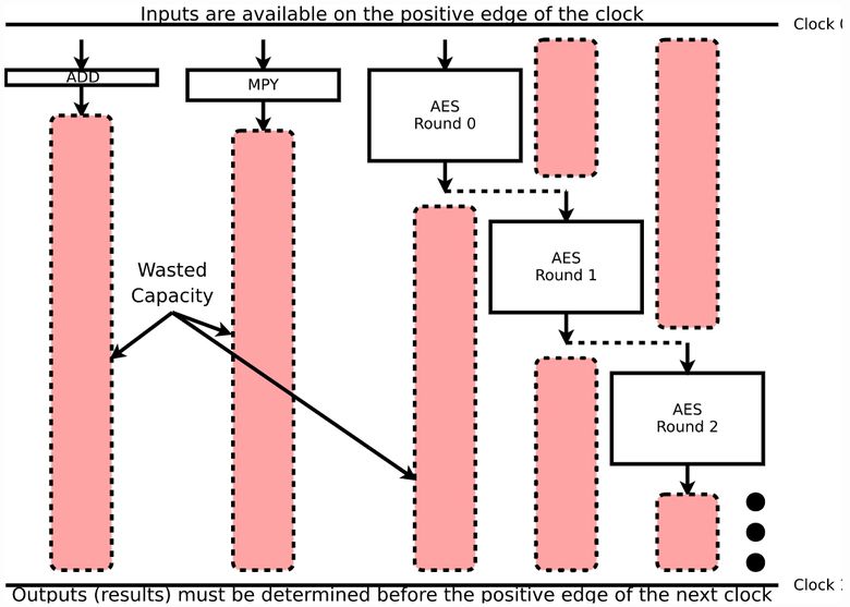
Figure 5 shows several operations (addition, multiplication) and several rounds of using AES, although for our example these could be rounds of any other algorithm. The vertical size of the blocks characterizes the duration of each operation. In addition, operations that depend on other operations follow each other. That is, if you want to perform many rounds of AES use within a tact, then keep in mind that the second round will not start until the first round is completed. Therefore, the introduction of such logic will increase the duration between tick ticks and slow down the total clock frequency.
Look at the pink blocks.
They reflect the loss of activity of your hardware circuit (hardware circuit) - the time that could be spent on performing some operations. But since you decide to wait for the end of a clock or wait to process the input data first, you cannot do anything. For example, on this graph, multiplication lasts no more than one round of AES, as well as addition. However, you cannot do anything with the results of these two operations while AES calculations are being performed, because you need to wait for the next clock cycle to get their next input. That is, pink blocks are idle time of the electronic circuit. And in this case, it is increased due to the fact that the AES rounds postpone the next beat. So this scheme will not be able to use all the capabilities of the equipment.
If we only needed an AES application pipeline, so that one round could be computed in each cycle, then the scheme could work faster, spending less time waiting.
Figure 6. Splitting operations to speed clocks
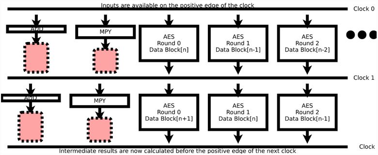
After splitting the operation into smaller operations, each of which can be performed between tick ticks, the loss of activity is greatly reduced. And instead of encrypting only one block of data at a time, we can turn the encryption algorithm into a pipeline. The resulting logic will not encrypt a single block faster than in Figure 5, but if you keep the pipeline full, this will increase the AES encryption speed by 10-14 times.
This is a consequence of better architecture.
Is it possible to do even better? Yes! If you are familiar with AES, then you know that each round consists of discrete steps. They can also be scattered, even more increasing the speed of the tact, until the execution of the AES-round logic takes less time than the multiplication. This will increase the number of additions and multiplications that you can perform, so decomposing the encryption engine into microconveyors will allow even more data to pass per cycle.
Not bad.
Figure 6 also shows a couple of other things.
First, we will consider the arrows as delays in routing (routing delays). The graph is not large, it is just an illustration for an abstract discussion. Each part of the logic should receive the result of the previous part of the logic. This means that even if some part of the logic does not take time to execute - as if the order of the wires just changed - then switching the logic from one end of the chip to the other will still take time. Therefore, even if you simplify your operations as much as possible, there will still be delays in moving data.
Secondly, you may have noticed that no arrow starts from the beginning of the measure. And no one comes to the next measure. This is done to illustrate the concept of setup and hold timing. Triggers are structures that hold and synchronize your data in tact. They need time before the start of the cycle, so that the data become permanent and defined. Although many believe that the beat begins instantly, in fact it is not. In different parts of the chip, it starts at different times. And this also requires a buffer between operations.
What conclusions can be drawn from this lesson?
- Performing logic takes time.
- The more logic, the more time is needed.
- The speed of a clock is limited by the amount of time it takes to execute the logic between clock ticks (plus routing delays, setup and hold times, uncertainty at the start of a clock, etc.).
The more logic in the clock, the lower the clock frequency. - The speed of the fastest operation will be limited by the speed of the tact needed to perform the slowest operation.
For example, the above addition operation. She could have done faster than multiplication and any single round of AES, but she had to wait for the rest of the logic in the scheme to be executed. - There is a hardware clock speed limit. It takes some time even for operations that do not require logic.
It turns out that with a balanced architecture, a more or less equal amount of logic needs to be located in cycles throughout the entire circuit.
How much logic to put in cycles?
Now you know that you need to work with bars. How do you modify or build your circuit in the light of this information? The correct answer is: you limit the amount of logic in clock cycles. But how much to limit and how to understand it?
One way to determine the optimal amount of logic in a clock is to set an average of the speed of the clock, and then build a circuit using a set of tools that your hardware understands. Every time the circuit does not meet the timing requirements, you will have to go back and break the circuit components or slow down the clock frequency. You need to be able to use your design tools to find the longest path.
Having done this, you will learn a number of heuristic rules, which you will then use to calculate the amount of logic in ticks applied to the equipment with which you work.
For example, I want to build a circuit with a clock frequency of 100 MHz with details of the Xilinx 7 series. These circuits then usually operate at 80 MHz and on Spartan-6 or 50 MHz and on iCE40 - although these are not strict combinations. On one chip, it will go fine, the other chip will turn out to be excessively powerful, on the third there will be problems with the timing check.
Here are some sample heuristic rules related to clocks. Since this is a heuristic, it is hardly applicable for all types of schemes:
1 . Usually, I can perform a 32-bit addition with multiplexing 4–8 elements within a clock cycle.
If you use faster clocks, for example 200 MHz, then you may need to separate the addition from the multiplexer. The longest ZipCPU path begins with the ALU output and ends with the ALU input. It sounds easy. Even corresponds to the above described heuristics. The problem that ZipCPU is struggling with at higher speeds is to route the output back to the ALU.
Let's take a look at the route: after ALU, the logical path first goes through a four-way multiplexer to decide which output to write back — from the ALU, the memory, or the division operation. The recorded result is then transferred to the bypass circuit to determine if it should be immediately transferred to the ALU as one of the two inputs. Only at the end of this multiplexer and traversal is the ALU operation and multiplexer finally performed. That is, at each stage a logical path can pass through the ALU. But thanks to the ZipCPU design, any clocks inserted in the logical path will proportionally slow down the execution of the ZipCPU. This means that the longest path will most certainly remain the longest ZipCPU path for a while.
If I was interested in running ZipCPU at a higher speed, then this would be the first logical path that I would try to break and optimize.
2. 16 × 16-bit multiplication takes only one clock. Sometimes on some hardware I can implement 32 × 32-bit multiplications in one clock cycle. And on the other equipment will have to break into pieces. So if I ever need a signed (signed) 32 × 32-bit multiplication, I will use the pipelined routine I have done for such cases. It contains several multiplication options, which allows me to choose the appropriate options for the current equipment.
Your hardware may also initially support 18 × 18-bit multiplications. Some FPGAs support multiplication and accumulation within one optimized hardware clock cycle. Examine your equipment to find out what features are available to you.
3. Any block access to RAM (block RAM access) takes one clock cycle. Try not to tweak the index during this tact. Also avoid any output operations at this time.
Although I argue that this is a good rule, I had to successfully break both its parts without (serious) consequences when operating at 100 MHz on the Xilinx 7 device (iCE40 has this problem).
For example, ZipCPU reads from its registers, adds an immediate operand to the result, and then selects whether the result should be a register plus a constant, PC plus a constant, or a condition code register plus a constant — all in one measure.
Another example: for a long time, Wishbone Scope determined the address to read from its buffer based on whether it was reading from memory during the current clock cycle. Breaking this dependency required adding one more clock cycle, so the current version no longer violates this rule.
These rules are nothing more than heuristics, which I use to determine how much logic fits in tacts. It depends on the equipment and the speed of the clock, so you may not be suitable. I recommend to develop their heuristics.
Next steps
Perhaps the best advice that I can give to FPGA beginner developers in the end is to study HDL, while practicing in parallel on real equipment, and not on simulators alone. Tools related to real hardware components will allow you to check the code and the necessary timings. In addition, it is good to develop circuits for fast clocks, but in the hardware design this world has not come together with a wedge.
Remember, hardware architecture is parallel in nature. It all starts with tact.
')
Source: https://habr.com/ru/post/339688/
All Articles