Count to three: four
Testing the viability of the idea: single-digit calculator
This is the fourth article, to the extent it is ready to be continued. Table of contents:
- We count to three: time (ternary multiplexer and adders)
- We count to three: two (memory)
- We count to three: three (counters)
- We count to three: four (one-digit computer and a three-team command system)
This is what the main piece of hardware looks like, which will be discussed today (more jumpers to the god of jumpers!):

The near future: a system of commands three-digit computer
As I said, my goal is to build, albeit a primitive, but tangible, programmable piece of hardware that works on ternary logic. So far, I am inclined to the following system of commands proposed here :
')
- each instruction will be a fixed length (5 trit)
- two tritas for the instruction identifier, three tritas (one triad) for its parameter
NN (-4) - expansion for the future (addition / subtraction with carry / borrow, skip the next command depending on the flag flag and the transfer flag, etc.)
NO (-3) - transfer control to ttt (in the future, you can switch segments through the R13 register)
NP (-2) - execute OPB ttt (universal binary command) on R1 and R2 (two other triads specifying the command are taken from R3 and R4) and set the flag of the sign
ON (-1) - execute OPA ttt (universal unary command) on R1 (write the result to the same R1) and set the flag of the sign
OO (0) - copy registers (see below)
OP (+1) - write the triad in the register R1
PN (+2) - write the triad in the register R2
PO (+3) - write the triad in the register R3
PP (+4) - write the triad in the register R4
Copy registers:
OONNN - copy R1 to R13
OONNO - copy R1 to R12
OONNP - copy R1 to R11
OONON - copy R1 to R10
OONOO - copy R1 to R9
OONOP - copy R1 to R8
OOPON - copy R1 to R7
OOPOO - copy R1 to R6
OOPOP - copy R1 to R5
OOONN - copy R1 to R4
OOONO - copy R1 to R3
OOONP - copy R1 to R2
OOOON - decrement R1 and set the flag flag
OOOOO - check R1 and set the sign flag
OOOOP - increment R1 and set the flag flag
OOOPN - copy R2 to R1
OOOPO - copy R3 to R1
OOOPP - copy r4 to r1
OOPNN - copy R5 to R1
OOPNO - copy R6 to R1
OOPNP - copy R7 to R1
OOPON - copy R8 to R1
OOPOO - copy R9 to R1
OOPOP - copy R10 to R1
OOPPN - copy R11 to R1
OOPPO - copy R12 to R1
OOPPP - copy R13 to R1
Please note that copying is performed only from / to the R1 register. Copying between other registers will have to be done in two teams, but on the other hand, the three parameters of the copy command of the OO allow me to address as many as 13 registers.
The instruction memory will be executed by three-position switches. Since the immediate parameter of the instruction is three-digit, the memory of commands will be addressed only in three matches, which gives 27 instructions, which is not enough. Therefore, there will be several segments of instruction memory, and the R13 register will be used to switch between segments, which gives a six-digit address bus, and the actual amount of instruction memory will be limited only by how much I get tired of soldering this memory.
One segment of the memory of teams will be recruited from fifteen of these scarves:

Each of these shawls carries 9 three-position switches, for clarity (especially in the photo), the commands are illuminated by two-color LEDs.
But before rushing into the rations of gigantic quantities (several hundred) of trimux, let's first try to make some much simpler calculator just to confirm that something can be built on this principle.
Case of the present: single-digit computer
So, simplify to the maximum. Our computer will have a total of nine teams, each of which is given by senior I and junior three J :
Ij
NN - copy R1 to R4
NO - copy R1 to R3
NP - copy R1 to R2
ON - decrement R1 and set the flag flag
OO - check R1 and set the flag flag
OP - increment R1 and set the flag flag
PN - copy R2 to R1
PO - copy R3 to R1
PP - copy r4 to r1
Nine teams are able to address a maximum of four memory registers, so that the memory will be four single-length registers and a flag flag. There will be no memory of commands in the calculator at all, which means that the pointer of the current command (counter) is not needed.
We collect registers
I will assemble the piece of iron and test each of its parts separately. Firstly, with such a number and density of wires, the probability of installation error is very high, and secondly, our eastern partners often sell not very high-quality jumpers :)
So, we will have four identical memory cells with memorization by level, we discussed them in detail in the second article:

It is difficult and irrational to bring access to all cells out, so they will be addressed through a one-to-four multiplexer. Of course, this is just a stripped-down version of a 1-to-9 multiplexer. As a result, the scheme of our memory is as follows:
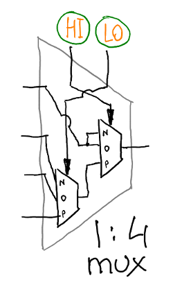
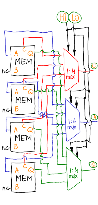
That is, the register memory is a piece of hardware, which takes two addresses to the input, and the output provides the legs C, A, Q of the corresponding memory cell. Here is a test of access to registers:
We address the right registers at the right moment.
All copying of registers will occur through an intermediate buffer. That is, first the contents of the register are copied to the buffer, and then the buffer is copied to the final register. My single-digit computer will be clocked with a ternary saw, the negative level will be copied to the buffer, and positively back from the buffer to memory.
This scheme allows you to address the desired memory register at the right time, depending on the instruction number IJ and the signal of the ternary saw CLK .
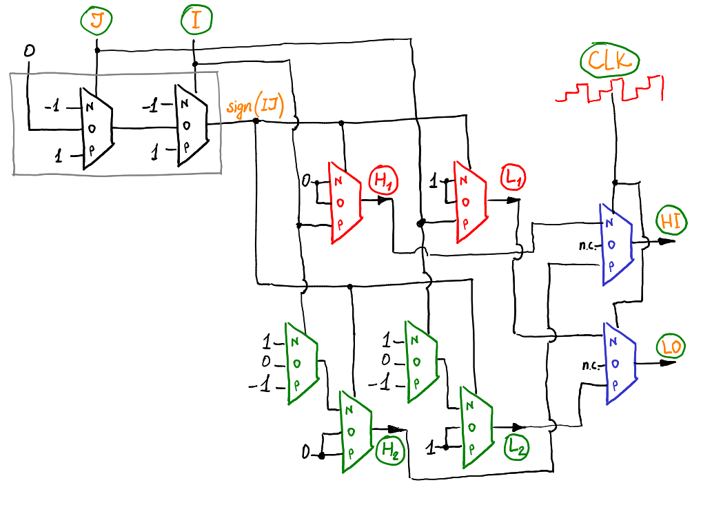
Red multiplexers generate the address of the cell from which to copy, green multiplexers give the address of the cell that is being written to. The blue multiplexers switch between them depending on the CLK signal.
Here is a video testing the operation of the memory addressing scheme:
Directly copying
Since the generation of the necessary memory addresses occurs on its own using the above scheme, in order not to overload the scheme, we can forget about the fact that we have four registers and imagine that there is only one register + buffer in memory.
Copying from register to buffer and back can be done extremely primitively:
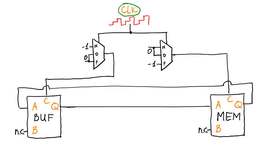
On the negative signal CLK on the leg C of the buffer will come -1, and on the leg of C memory will be 0, which means that the buffer will remember what it is served on leg A. On the positive signal CLK everything is exactly the opposite, copy the contents of the buffer back in memory.
Now it remains to remember that we have not only copy commands, but also commands to increase / decrease the register R1 by one. The final scheme of our computer looks like this:
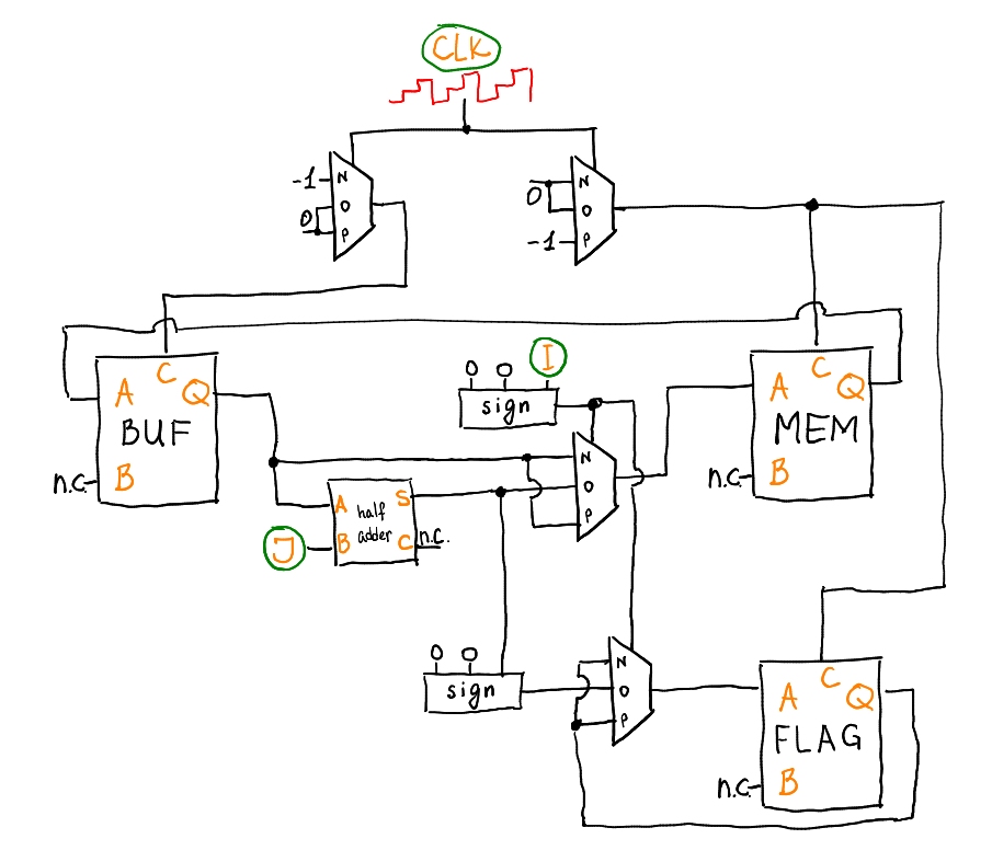
When the higher trit command is non-zero, the output of the Q buffer is fed directly to the input A of the memory. When it is zero, the output Q of the buffer is fed into memory through a half-adder (see the first -half scheme for a half-adder). Similarly, the setting of the sign flag occurs.
Well, this is what the piece of iron looks like:
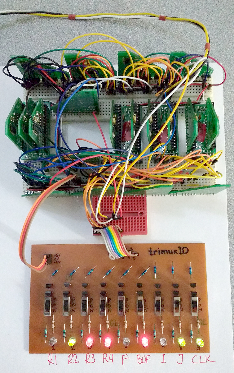
But the video of her testing:
Testing each brick separately is very useful, here are all the dead bridges that were found in the process of assembling only this piece of iron (hello to our eastern partners!)

Summarize
In principle, how to assemble the final three-digit calculator is quite clear, you just have to get up the courage and do it, and, of course, not on a breadboard, since, according to rough estimates, I will need hundreds of three or four trimux for it.
If it is rough, then the ALU of a three-rait computer will contain three times the last scheme (one for each trit). This, of course, does not end, since the ALU will contain a separate scheme for each team. Total you need to develop the remainder of the ALU, add more registers, add a command counter, memory of instructions, and directly the instruction decoder circuit. Nothing too heavy.
I will be glad to hear new ideas and comments!
Source: https://habr.com/ru/post/337606/
All Articles