SDAccel - check data transfer
In the previous article “SDAccel - first acquaintance” I tried to describe the basics of using OpenCL on Xilinx FPGAs. Now it is time to share the results of experiments on data transfer on the ADM-PCIe-KU3 module. Data transfer in both directions is checked. The source code of the programs is posted on GitHub: https://github.com/dsmv/sdaccel
Equipment
All experiments were performed on Alpha-Data module ADM-PCIe_KU3.

The central element is the FPGA Xilinx Kintex UltraScale KU060
Two SODIMM DDR3-1600 modules are connected to the FPGA; The memory width is 72 bits, this makes it possible to use a memory controller with error correction.
It is possible to connect two QSFP modules. Each QSFP module is four bidirectional lines with a transmission rate of up to 10 Gbit / s. This makes it possible to use 1G, 10G, 40G Ethernet, including the implementation of Low-Latency Network Card. There is also an interesting feature - entering the second label from the GPS receiver. But in this paper, all this is not used.
NIMBIX server
The NIMBIX server provides various computing services, including the SDAccel development environment and, more importantly, the execution of the program on the selected hardware module.
Calculator model
I want to remind you what the OpenCL system is.
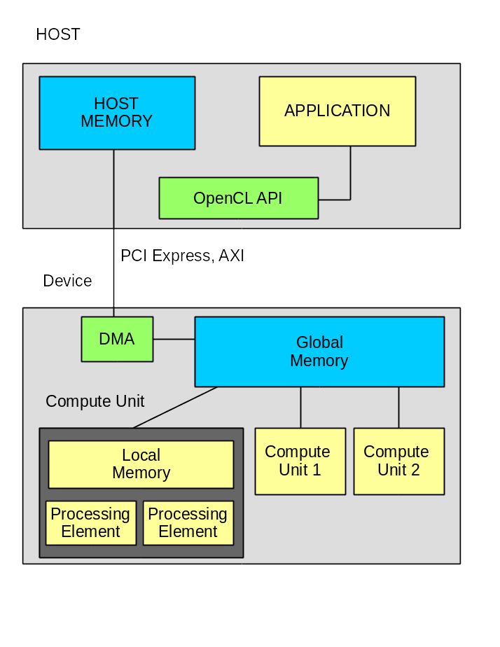
The system consists of HOST computer and computer, which are interconnected by bus. In this case, it is PCI Express v3.0 x8;
Application software consists of two parts:
- Program HOST computer.
- One or more functions to work on the computer.
Data exchange takes place only through global memory, in this case it is two SODIMM modules.
The application software requires infrastructure that someone must provide. In this case, the company Xilinx. The infrastructure includes:
- opencl library - implementation of OpenCL standard functions.
- module driver - provides interaction with the module.
- DSA package. This is the basis for developing your own firmware FPGA.
The DSA package contains basic firmware, which includes controllers for PCI Express, dynamic memory, and possibly for other nodes. The basic firmware contains an element called OpenCL Region. It is within this element that all the functions of the OpenCL kernels will be implemented. Firmware uploads into OpenCL Regions are done via PCI Express using Partial Reconfiguration technology. It should be noted that Xilinx has greatly advanced in download speed. If in previous versions the download took a few minutes, then what is now about 5 seconds. And in version 2017.2 it is announced that it is possible not to reload the firmware at all.
Currently, there are two packages available for the ADM-PCIe-KU3 as part of the SDAccel package:
- xilinx: adm-pcie-ku3: 2ddr: 3.3
- xilinx: adm-pcie-ku3: 2ddr-xpr: 4.0
Both packages have support for two memory controllers and PCI Express v3.0 x8; Note the suffix -xpr. This is quite an important distinction. Option without xpr fixes the position of DDR controllers and PCI Express. The version with xpr captures only the position of PCI Express, and the DDR controllers are involved in tracing OpenCL application functions. This difference leads to differences in results. A variant without xpr is divorced faster, and a variant with xpr can get a more optimal trace. For this project, it turned out 1 hour 11 minutes for the option without xpr and 1 hour 32 minutes for the option xpr. Logs here .
By the way, each DSA package includes its own driver.
Program CHECK_TRANSFER
The program is designed to test the continuous transmission of data in three modes:
- From FPGA to SODIM and to computer
- From computer to SODIMM and to FPGA
- Simultaneous transmission in two directions
In my opinion, checking the speed of work without checking the data does not make much sense. Therefore, using OpenCL, I implemented a FPGA node for the test sequence generator and a test sequence for the test sequence node.
The OpenCL standard provides for the exchange between a device and a computer only through the device’s global memory. This is usually SODIMM dynamic memory. And here a very interesting question arises about the possibility of transferring data with speed limits. On the ADM-PCIe-KU3 module, two SODIM DDR3-1600 are applied. The exchange rate for one SODIMM is about 10 GB / s. The exchange rate on the bus PCI Express v3.0 x8 - about 5 GB / s (so far it turned out much less). Those. It is possible to write into memory one block coming from PCI Express and simultaneously read the second block for processing inside the FPGA. What to do if you still need to return the result? PCI Express provides bidirectional streaming at high speed. But the memory has one bus, and the speed will be divided between reading and writing. This is where the second SODIMM is needed. We have the opportunity to specify in which module the buffer will be placed for processing.
operating system
SDAccel can only work under some Linux systems. In the list of available systems CentOS 6.8, CentOS 7.3, Ubuntu 16.04, RedHat 6.8, RedHat 7.3; The first experiments I started on CentOs 6.7; Then I tried to use Ubuntu 16.04, but it didn’t work there. At the moment I am using CentOS 7.3 and am very pleased with this system. However, when setting up SDAccel there are a number of subtleties. The main problem is that the default network interface name is “enp6s0”. This name does not understand the Xilinx license server. He needs the usual “eth0”.
Setting up here: https://github.com/dsmv/sdaccel/wiki/note_04---Install-CentOS-7-and-SDAccel-2017.1
Qt 5.9.1 is installed but not working. It requires a newer gcc and git compiler. This is also solved, the details here: https://github.com/dsmv/sdaccel/wiki/note_05---Install-Qt-5.9.1-and-Git-2.9.3
Development systems
For development I use two systems:
- SDAccel 2017.1 - for the development of kernel and small test programs HOST
- Qt 5.9.1 - for developing more complex programs. Qt is used only for developing HOST programs.
Project organization on GitHub
The dsmv / sdaccel repository is designed to develop examples for SDAccel. At the moment there is only one program check_transfer. The project uses a number of GitHub features:
- README.md - the first file that is visible to the visitor.
- WiKi - program description
- Development Notes - notes on development
- Issues - task list
- Projects - project management
- And also there is documentation on the program formed by Doxygen
The main directories of the program
- useful - useful scripts to customize the system
- qt - directory for Qt sources
- sdx_wsp / check_transfer - SDAccel working directory
In this project, the sources for Qt and SDAssel are the same, although they are in different directories. However, it is assumed that Qt will develop much more complex programs.
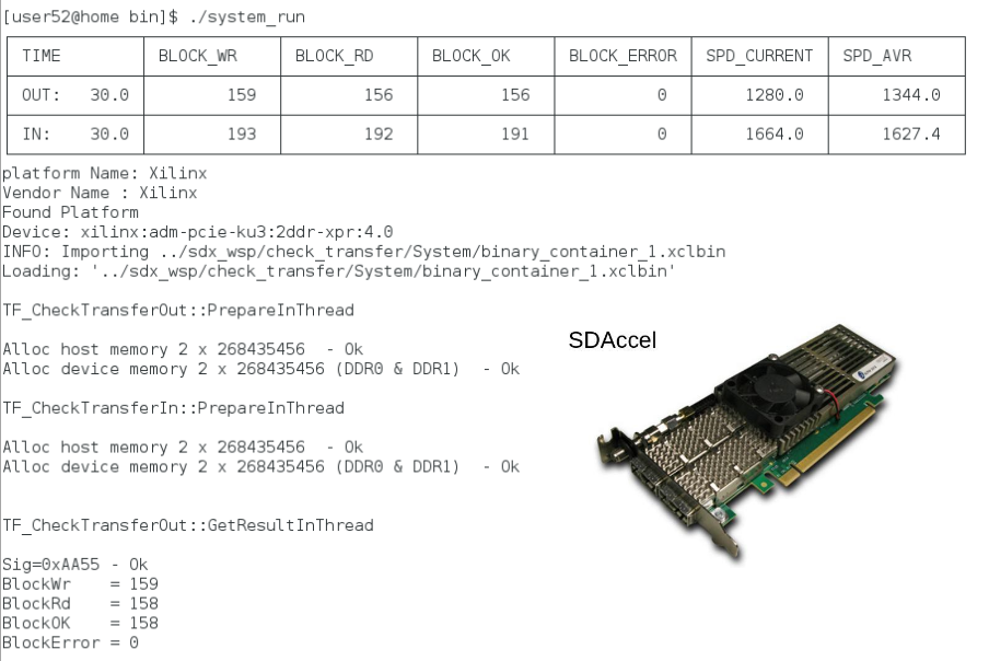
Two output modes
(Click on image to enlarge)
The figure shows the appearance of the terminal while the program is running. Pay attention to the table. This is a table with the current status of the test. While working, it is very interesting to know what actually happens. Moreover, there is a mode without time limit. The table helps a lot. Unfortunately, there are problems. SDAccel is based on Eclipse. I did not manage to learn how to run the program from the environment in an external terminal. And in the built-in terminal the table does not work. I had to make a run mode without a table. By the way, the Nsight Eclipse Edition system for programming NVIDIA devices is also not able to run programs in an external terminal. Or maybe I do not know something?
Megabytes or mebabytes?
I belong to those people who know for sure that 1 kilobyte is 1024 bytes (and also assume that at 1 kilometer 1024 meters). But it is already illegal. To avoid confusion, the program can measure in both modes and the current mode is displayed in the log.
Let's look at some pieces of program code.
Kernel gen_cnt
The kernel code gen_cnt () is very simple. The function fills an array of a given size with a test data block.
__kernel __attribute__ ((reqd_work_group_size(1,1,1))) void gen_cnt( __global ulong8 *pOut, __global ulong8 *pStatus, const uint size ) { uint blockWr; ulong8 temp1; ulong8 checkStatus; ulong8 addConst; checkStatus = pStatus[0]; temp1 = pStatus[1]; addConst = pStatus[2]; blockWr = checkStatus.s0 >> 32; __attribute__((xcl_pipeline_loop)) for ( int ii=0; ii<size; ii++) { pOut[ii] = temp1; temp1.s0 +=addConst.s0; temp1.s1 +=addConst.s1; temp1.s2 +=addConst.s2; temp1.s3 +=addConst.s3; temp1.s4 +=addConst.s4; temp1.s5 +=addConst.s5; temp1.s6 +=addConst.s6; temp1.s7 +=addConst.s7; } blockWr++; checkStatus.s0 = ((ulong)blockWr)<<32 | 0xAA56; pStatus[0] = checkStatus; pStatus[1] = temp1; } The variable temp1 is of type ulong8. This is the standard OpenCL type which is a vector of eight 64-bit numbers. You can refer to the elements of the vector by the names s0..s7 or so temp1.s [ii]. It is quite convenient. The width of the vector is 512 bits. This corresponds to the width of the internal bus for the SODIMM controller. One of the elements of optimization is the exchange with only 512 bit data with memory. According to the pStatus pointer, a block with status information is located, the current value and constants are read from it. For each 64-bit field, its own constant is used. This allows you to make not only a simple counter, but also something more complicated. Although so far the program makes only a simple counter. At the end of the function, the current data value and the number of filled blocks are recorded.
check_cnt_m2a and check_read_input
To implement the check, I wrote two functions, one check_read_input - reads data from the dynamic memory and writes them to the pipe. The second, check_cnt_m2a, reads the data from the pipe and checks it. Probably in this case, the division into two kernels and their connection through the pipe is redundant. But it was interesting for me to test this technology.
Code here
HOST program structure
The program is based on the use of virtual classes TF_Test and TF_TestThread ; Based on these classes, two testing classes have been developed.
- TF_CheckTransferOut - check transfer from device to computer
- TF_CheckTransferIn - check transfer from computer to device
The base class TF_Test contains functions:
| Title | Purpose |
|---|---|
| Prepare () | Training |
| Start () | Launch |
| Stop () | Stop |
| StepTable () | Table display step |
| isComplete () | Test completed |
| GetResult () | Output |
The main () function creates one instance of each class and starts execution.
Each testing class creates its own flow of execution, in which it is exchanged with the module. The main function calls Prepare () for each class. Inside this function, a stream is created, memory is allocated and all the preparation is done. After both classes are ready, a start is called, which causes the main testing cycle to start. When you press Ctrl-C or at the end of a specified test time, Stop () is called. Classes stop their work and using the isComplete () function inform main () about it. After stopping, GetResult () is called to get the result. During the test, the main () function calls a StepTable every 100 ms to update the table. This allows you to update status information without interfering with the data exchange.
This approach turned out to be very convenient for building test programs. Here, all tests are built on the same template. As a result, they can be run in parallel, or one by one. This program easily organizes the mode of both a single run of one of the tests and a simultaneous start.
Modes of execution of the OpenCL program
The SDAccel system provides three program execution modes:
- Emulation-CPU - everything runs on a HOST processor
- Emulation-HW - OpenCL functions are performed on the Vivado simulator
- System - work on real hardware.
In more detail - in the previous article .
It is interesting to compare the speed of work in three environments. The comparison is very revealing:
| Emulation CPU | Emulation-hw | System |
|---|---|---|
| 200 MB / s | 0.1 MB / s | 2000 MB / s |
I rounded the numbers to see the order better. Actually, the speed difference between Emulation-CPU and Emulation-HW shows that in the development of FPGA firmware it is necessary to switch to C / C ++ or something similar. Winning four orders of magnitude is a lot, it covers all the drawbacks of C ++. It should be noted that the development of VHDL / Verilog will not disappear, and these languages will most likely have to be used to achieve maximum performance. The possibility of creating an OpenCL kernel on VHDL / Verilog looks very promising; this will allow combining high speed of development and limiting characteristics of the FPGA. But this is a topic for a separate study and a separate article.
Trace result
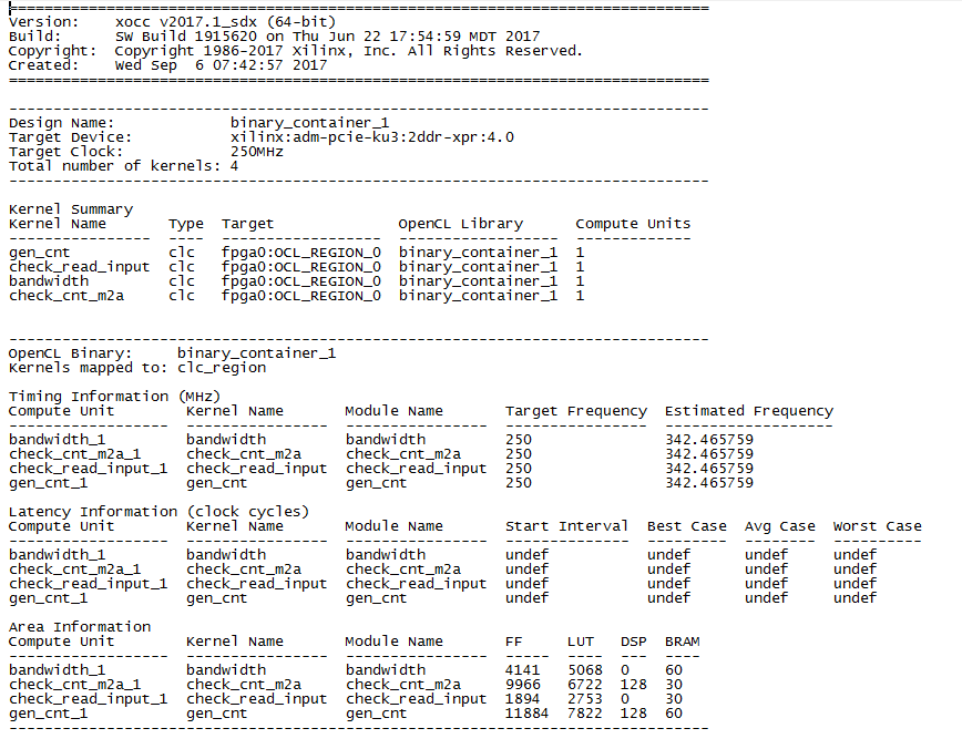
That's what happened. Note the number of DSPs for gen_cnt. To implement eight 64-bit counters, 128 DSP blocks were required. This is 16 blocks per counter. Most likely this is the result of the work of the optimizer on the disclosure of the cycle.
Differences in optimization methods for FPGA and GPU
To achieve maximum results, different optimization methods should be applied. GPU has a fixed structure. If, conditionally speaking, one processor element of a GPU can perform one operation, then in order to perform 100 operations in parallel, 100 processor elements must be used. But in FPGA it is not the only option. Yes, we can write one kernel and place several copies in the FPGA. But this leads to a lot of overhead. Xilinx recommends using no more than 16 kernel, or rather memory ports. But inside one element there are no restrictions on parallelization. Actually the gen_cnt example shows this. There immediately in the code eight 64-bit adders are recorded. In addition, the optimizer worked and launched a cycle. For a GPU, this example should be written differently, for example, make one kernel to get a 64-bit sample and run eight instances at once.
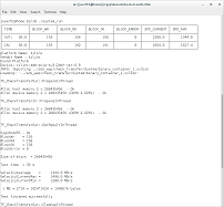
What Emulation-HW can show
This mode can show what is happening on the memory access bus. The picture shows the process of reading data from memory function check_read_input ().
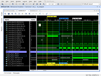
(Click to enlarge)
First of all, you can see how long the data is coming. The delay from the first request until the first data 512 ns. Secondly, it is clear that the reading is in blocks of 16 words (512 bits in size). When developing on VHDL, I would use a larger block size. But apparently the controller is able to combine the blocks and this does not lead to a slowdown. In the third it is clear that there are gaps in data acquisition. They are also explicable. The frequency of OpenCL 250 MHz, the memory bus frequency for SODIMM DDR3-1600 is 200 MHz. The gaps correspond exactly to the transition from the 200 MHz bus to the 250 MHz bus.
results
The results are interesting, but I expected to achieve higher speeds.
Single tests
| Computer | Enter [MiB / s] | Conclusion [MiB / s] |
|---|---|---|
| Intel Core-i5, PCIe v2.0 x8 | 2048 | 1837 |
| Intel Core-i7, PCIe v3.0 x8 | 2889 | 2953 |
Bidirectional test
| Computer | Enter [MiB / s] | Conclusion [MiB / s] |
|---|---|---|
| Intel Core-i5, PCIe v2.0 x8 | 1609 | 1307 |
| Intel Core-i7, PCIe v3.0 x8 | 2048 | 2057 |
For comparison, on our module with a similar FPGA the record input speed was 5500 MiB / s, although for several reasons it had to be reduced to 5000. So there are opportunities for increasing the exchange rate.
What's next
Work will continue.
- SDAccel 2017.2 exploration
- Implementation of the convolution node based on the FPFFTK library by Alexander Kapitanov ( capitanov )
- Develop your own DSA packages, including those with support for 10G Ethernet
- And most importantly - the development of its own module, the name already exists - DSP135P
PS I want to thank Vladimir Karakozov for his help in developing the testing program template.
')
Source: https://habr.com/ru/post/337568/
All Articles