Asynchronous circuit study in ModelSim
Read the article FPGA / Asynchronous decoder from ajrec .
I first read and understood nothing, and then I read it again and again did not understand anything. In fact, I have already read all the ajrec articles about asynchronous circuits and I have to state that I understand little of what this is all about (although I think that I have design experience in FPGA).
')
In the comments to the articles, the author basically gets disadvantages, people laugh and do not seem to understand as I do.
Honestly, I always look with curiosity on projects that are “not like everyone else.” I believe that only such projects have a chance to either sink deep or fly high. If you do something the same way as hundreds of other developers, then you go the beaten track, it is easy and comfortable here. Not everyone can take a step aside and go on their own path.
I tried to understand the design of the asynchronous decoder and at least make a temporary simulation of the code in ModelSim. Further about what came of it.
Frankly speaking, the article “ Asynchronous decoder ” and “ Petrify's self-timed synthesis system: problems and their solutions ” is not good in my head. I am thoroughly "spoiled by the synchronous design technique."
In addition, the article has oddities that cut the eye. Here, for example, quote:
Output signals:
q1 - switches if r1 = 1 and r2 = 1;
q2 - switches if r1 = 1 and r2 = 0;
q3 - switches if r1 = 0 and r2 = 1;
q4 - switches if r1 = 0 and r2 = 0.
I probably find fault with myself, but I can hardly imagine a programmer who writes the numbering of signals starting with one and that q4 switches when r1 = 0 and r2 = 0. In my head everything is strictly according to the pattern: {0, 0} - corresponds to the signal q0. {0, 1} - corresponds to the signal q1. {1, 0} - corresponds to the signal q2 and {1, 1} - corresponds to the signal q3. But this, of course, little things that are irrelevant.
The main claim on my part: the author does not test his hypotheses / studies / projects in the FPGA or in any other way. He writes: "I do not have the opportunity to test the circuit in a real embodiment." Well, how is that?
Actually, this prompted me to try to simulate the logic of the decoder described by ajrec . Temporary simulation is a fairly good model that will show the behavior of the circuit in a real FPGA. True ... there is a nuance - I do not have complete confidence that ModelSim will be able to reliably simulate asynchronous circuits: the ModelSim simulator is intended primarily for the “traditional” synchronous design.
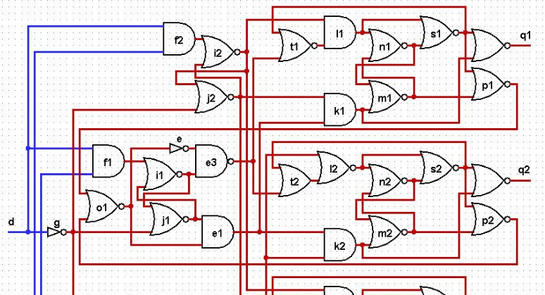
So. The source code from the article FPGA / Asynchronous decoder we do not know what language and looks like this:
e=NOT(o1); e1=AND(o1,j1); e2=AND(o2,h1); e3=NAND(e,i1);
e4=OR(o2,h1); f1=AND(d,r1); f2=AND(d,r2); g=NOT(d);
h1=NOR(g,r1); h2=NOR(g,r2); i1=NOR(f1,j1); i2=NOR(f2,j2);
j1=NOR(g,i1); j2=NOR(g,i2); k1=AND(e1,j2); k2=AND(e1,h2);
k3=AND(e2,j2); k4=AND(e2,h2); l1=AND(t1,i2); l2=NOR(t2,h2);
l3=AND(t3,i2); l4=NOR(t4,h2); m1=NOR(k1,n1); m2=NOR(k2,n2);
m3=NOR(k3,n3); m4=NOR(k4,n4); n1=NOR(l1,m1); n2=NOR(l2,m2);
n3=NOR(l3,m3); n4=NOR(l4,m4); o1=NOR(p1,p2); o2=NOR(p3,p4);
p1=NOR(m1,s1); p2=NOR(m2,s2); p3=NOR(m3,s3); p4=NOR(m4,s4);
s1=NOR(n1,l1); s2=NOR(n2,l2); s3=NOR(n3,l3); s4=NOR(n4,l4);
t1=NOR(e3,s1); t2=OR(e3,s2); t3=NOR(e4,s3); t4=OR(e4,s4);
q1=NOR(s1,k1); q2=NOR(s2,k2); q3=NOR(s3,k3); q4=NOR(s4,k4).
Further in the article there is an equivalent circuit of this thing and it is said that generally the signals m1, m2, m3, m4 must also be reset to the initial state before starting work. Well, I’ll rewrite it all to Verilog like this:
module test( input wire d, input wire r1, input wire r2, input wire set0, output wire q1, output wire q2, output wire q3, output wire q4, output wire [3:0]qq ); wire e, e1, e2, e3, e4; wire f1, f2; wire g; wire i1, i2; wire j1, j2; wire h1, h2; wire k1, k2, k3, k4; wire l1, l2, l3, l4; wire m1, m2, m3, m4; wire n1, n2, n3, n4; wire o1, o2; wire p1, p2, p3, p4; wire s1, s2, s3, s4; wire t1, t2, t3, t4; function NOT; input s; begin NOT=~s; end endfunction function AND; input s1,s2; begin AND=s1&s2; end endfunction function NAND; input s1,s2; begin NAND=~(s1&s2); end endfunction function OR; input s1,s2; begin OR=s1|s2; end endfunction function NOR; input s1,s2; begin NOR=~(s1|s2); end endfunction assign e=NOT(o1); assign e1=AND(o1,j1); assign e2=AND(o2,h1); assign e3=NAND(e,i1); assign e4=OR(o2,h1); assign f1=AND(d,r1); assign f2=AND(d,r2); assign g=NOT(d); assign h1=NOR(g,r1); assign h2=NOR(g,r2); assign i1=NOR(f1,j1); assign i2=NOR(f2,j2); assign j1=NOR(g,i1); assign j2=NOR(g,i2); assign k1=AND(e1,j2); assign k2=AND(e1,h2); assign k3=AND(e2,j2); assign k4=AND(e2,h2); assign l1=AND(t1,i2); assign l2=NOR(t2,h2); assign l3=AND(t3,i2); assign l4=NOR(t4,h2); assign m1=NAND( set0, OR(k1,n1)); /* NOR(k1,n1); */ assign m2=NAND( set0, OR(k2,n2)); /* NOR(k2,n2); */ assign m3=NAND( set0, OR(k3,n3)); /* NOR(k3,n3); */ assign m4=NAND( set0, OR(k4,n4)); /* NOR(k4,n4); */ assign n1=NOR(l1,m1); assign n2=NOR(l2,m2); assign n3=NOR(l3,m3); assign n4=NOR(l4,m4); assign o1=NOR(p1,p2); assign o2=NOR(p3,p4); assign p1=NOR(m1,s1); assign p2=NOR(m2,s2); assign p3=NOR(m3,s3); assign p4=NOR(m4,s4); assign s1=NOR(n1,l1); assign s2=NOR(n2,l2); assign s3=NOR(n3,l3); assign s4=NOR(n4,l4); assign t1=NOR(e3,s1); assign t2=OR(e3,s2); assign t3=NOR(e4,s3); assign t4=OR(e4,s4); assign q1=NOR(s1,k1); assign q2=NOR(s2,k2); assign q3=NOR(s3,k3); assign q4=NOR(s4,k4); assign qq = 1 << {r2,r1}; endmodule I tried to make minimal changes to the source code in order not to accidentally break logic, which I do not understand. Therefore, I defined the Verilog functions AND, OR, NOR, NAND to do what they should do. The assignment of a signal value in Verilog is done through assign. If you need someone, here is a brief description of the language Verilog .
Thus, in the test module there are input signals of the decoded address r1 and r2, as well as a reset signal set0 and a signal d - a command for the operation of decoding the address (in the author’s terminology). The output signals are q1, q2, q3 and q4.
In addition, I added a gag, four-bit output qq, which is calculated by a traditional decoder, like this: assign qq = 1 << {r2, r1};
The test module was inserted into the Intel Quartus Prime Lite Edition v16.1 project for the FPGA IC Cyclone IV E.
The project was compiled. First, in the project settings Assignments => Settings => EDA Tools Settings => Simulation, you need to select the Tool Name => ModelSim-Altera. Then, after compilation, a simulation / modelsim folder will be created in which there will be the * .sdo and * .vo modules that are needed for the temporary simulation.
Now you need a testbench. I wrote it in a simple way:
`timescale 1ns / 1ns module tb(); reg r1_; reg r2_; reg d_; reg set_; wire q1_,q2_,q3_,q4_; wire [3:0]qq_; test test_inst( .d(d_), .r1(r1_), .r2(r2_), .set0(set_), .q1(q1_), .q2(q2_), .q3(q3_), .q4(q4_), .qq(qq_) ); initial begin $dumpfile("out.vcd"); $dumpvars(0,tb); //reset m1-m4 signals using "set_" r1_=0; r2_=0; d_=0; set_=0; #100; set_=1; #100; //check addr 00 r1_=0; r2_=0; #100; d_=1; #100; d_=0; #200; //check addr 01 r1_=1; r2_=0; #100; d_=1; #100; d_=0; #200; //check addr 10 r1_=0; r2_=1; #100; d_=1; #100; d_=0; #200; //check addr 11 r1_=1; r2_=1; #100; d_=1; #100; d_=0; #200; //-------------------- //check addr 00 r1_=0; r2_=0; d_=1; #100; d_=0; #200; //check addr 01 r1_=1; r2_=0; d_=1; #100; d_=0; #200; //check addr 10 r1_=0; r2_=1; d_=1; #100; d_=0; #200; //check addr 11 r1_=1; r2_=1; d_=1; #100; d_=0; #200; end endmodule Here, the address signals r1 and r2 are alternately set to all four possible values of 2'b00, 2'b01, 2'b10 and 2'b11, while this signal d is generated, which activates the decoding.
This all happens twice, the first four decryption activation signals d occur at steady-state signals r1 and r2, and in the second group of signals d comes simultaneously with signals r1 and r2. Honestly, I do not know how it really should be according to the intention of the author. That is why I consider such an extreme case, the arrival of the activation signal d at the moment of establishing the signals r1 and r2.
Now I run ModelSim-Altera (or now Intel). I create a project and workshop space. I add two existing files to it: a testbench tb.v and a compiled quarter project async_test.vo:
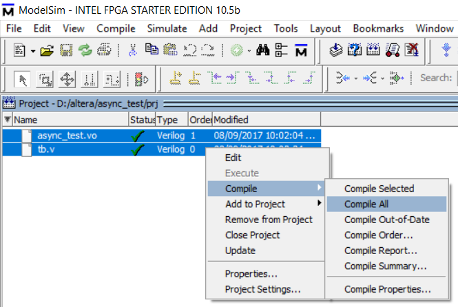
They now need to be compiled using ModelSim. Right mouse button and choose from the menu Compile All. It is necessary that there appear green check marks near each file. Sometimes there is a strangeness and ModelSim finds syntax errors where the quartet does not see them. This is so, by the way.
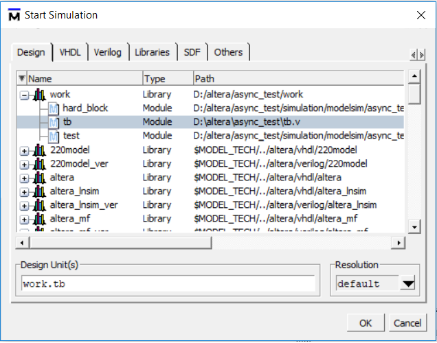
Now you can start the simulation through the ModelSim menu, Simulate-> Start Simulation ...
This is where the dialog box appears:
1) select the top module and now it is a testbench
2) add libraries altera
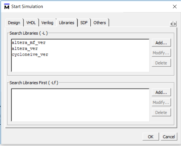
3) add the compiled SDF file, from which all temporary parameters will go

After successfully loading all the files and modules necessary for the simulation, we need to add the signals of interest to the time diagrams window.
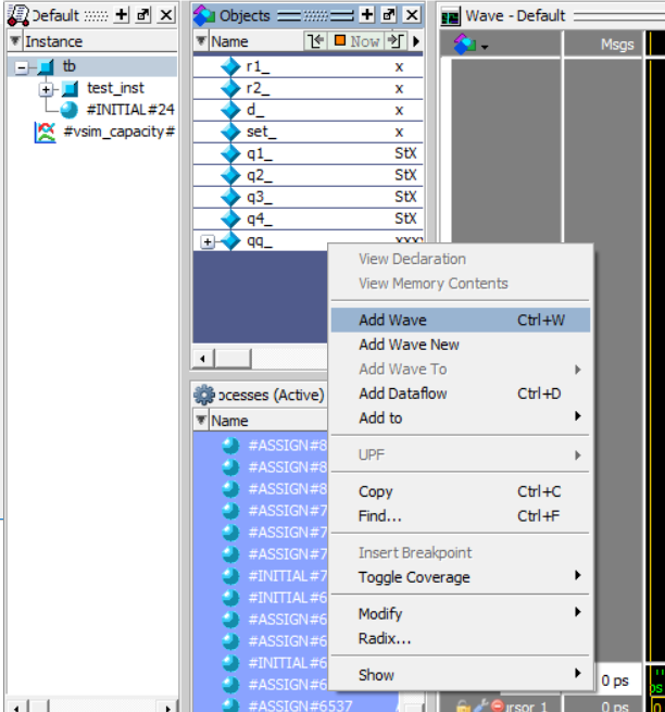
Click OK and then Simulate => Run => Run-all
So it happened - it worked!
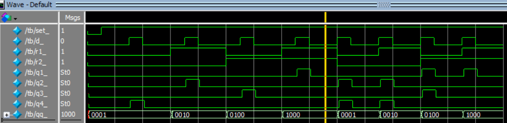
What I see:
First, the project seems to almost work and decodes addresses, as promised - only for the first group of four pulses d. Somehow the outputs of the decoder are confused, for {r2, r1} = 2'b01 q2 is ignited. But I already spoke about this oddity above. To be honest, I was very surprised that this generally works under some conditions.
The second group of 4 d pulses does not work correctly. This is the moment when the signal d arrives simultaneously with the changing r1 and r2.
Here I would like to more accurately understand the role of the signal d. In synchronous logic, I know there is a clock frequency that snaps data from one register to another through combinational functions. In this case, the developer is obliged to provide the so-called time parameters tsu and thold. Here is the first available picture on a topic from Google:
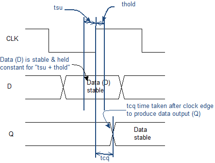
The signal latched in the register must be stable for some time tsu (setup time) up to the clock edge and some time after the thold clock edge (hold time). If this condition is not met, then the synchronous scheme does not work or does not work reliably (that is, it actually does not work).
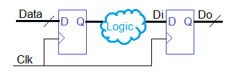
What is a stable signal? There is a register in which the input data is stored. Next comes the logic function, which from the input data (it can be several bits) calculates the next value, which is stored in the next register. So the logic function must calculate the result in a time less than the duration of the clock frequency period. Not only have time to calculate. Since there are several discharges, the result must still be in time to run along the conductors each to its latching register.
Now, going back to the asynchronous circuit and the d signal, I understand that the second group of four pulses d in this asynchronous circuit during simulation apparently does not work correctly for exactly the same reason that the synchronous circuit may not work either. Namely, not maintained tsu. The d signal comes when the r1 and r2 signals have not yet arrived or are not stable.
It seems to me that the author of the asynchronous scheme cannot avoid temporal analysis. Be sure to take care of the stability of the signals r1 and r2 before the arrival of d. It needs to be somehow controlled and taken into account. Honestly, the pulse itself d is somewhat reminiscent of a clock frequency clock. The signal d has a duration, so it means that this duration is provided by something, some kind of generator? It turns out that the asynchronous circuit still needs time-setting circuits, those that determine the duration and position of signal d? In general, the origin of this signal d is not very clear ...
I wanted to draw attention to a few more points in my simulation. Even when the circuit is working (the first 4 pulses d on the simulation), the output signals q1, q2, q3, q4 are shifted relative to the signal d and each is shifted by a different time. The most interesting is that the width of the pulses q1, q2, q3 and q4 is always greater than the width of the pulse d and they are all different in width. I do not know how the author is going to combine such schemes with one another. If we assume that the output signal q1 for the subsequent circuits becomes the signal d, then it turns out that through the chain of circuits the signal d becomes wider and wider - but this is already my fantasy. I repeat, I do not really understand how such schemes will be assembled into large ones.
Another thought does not leave me.
It seems to me that the traditional decoder is like the one I have above assign qq = 1 << {r2, r1}; It takes much less space in the chip in terms of the number of transistors than the asynchronous circuit described by the author. And the number of transistors in ASIC directly affects the performance, because it turns out a large area of the chip is occupied and longer paths between the elements, more power consumption. It is necessary to think about this, how to evaluate it and how to calculate it.
Sometimes I myself have strange “breakthrough” ideas on how to make electronics faster or use a “different principle” of work. Moore's law is somehow not very working, and to increase the speed of electronics, new ideas are required. In the case of microprocessors, this may be some fundamentally different architecture (hmm ... I have it). Or you need fresh technologies and ideas about the device basic elements of chips.
I once did experiments on the implementation of the scheme on the Double-Edge-Trigger. The idea was to use both clock edges for normal synchronous logic. I thought that using a DET trigger would allow the chip to have a working frequency of two times less for the same computing speed, which means that at least the power consumption will decrease. I stimulated my project and even launched it in FPGA - it worked. Details about this project here .
Then I tried to estimate the required number of transistors and came to a disappointing conclusion: it seems that the circuit with DET triggers will require much more than usual transistors in a chip.
Asynchronous logic, as an idea, is interesting. But, unfortunately, requires deep study. To real use is still too far and not obvious. And it is necessary to check the result even in FPGA, even in the simulation - it is not difficult and not expensive. It seems that ModelSim copes with the simulation of asynchronous circuits.
Simulation is free! Try gentlemen!
Source: https://habr.com/ru/post/335386/
All Articles