Asynchronous decoder
As promised in the previous article, this article will focus on the representation of operations on addresses in an asynchronous form. As an example, I will describe the address decryption operation. Immediately I want to prevent the insinuations that I encountered after the publication of the previous article. It's about a fully and asynchronous device. And please do not refer to the abstract of the Uzbek University. Supposedly an asynchronous decoder can be obtained from synchronous using simple manipulations. At the same time a question to those who claim that the asynchronous processor was made 20 years ago. How did you manage this without an asynchronous decoder?
So, about the asynchronous descrambler. After reflection, I came to the conclusion that the only sane way for the synthesis of an asynchronous decoder is a phased doubling of the address using the add-on scheme over two decoders that is half the size of the address. Prove that there is no alternative way, I do not undertake. But I can say that the alternative path (if there is one) is much more expensive in terms of the number of added new signals.
In view of the foregoing, the discussion in this article will deal with a two-digit decoder. How to double the width of an asynchronous decoder, the topic of the next article.
')
So, we will describe the initial behavior of a two-bit asynchronous decoder. Oddly enough, it is not difficult to do in the language of STG, and the point here is not even a small bit.

Input Signals:
d - signal - command for address decryption operation;
r1, r2 - signals of bits of the register of the address.
Output signals:
q1 - switches if r1 = 1 and r2 = 1;
q2 - switches if r1 = 1 and r2 = 0;
q3 - switches if r1 = 0 and r2 = 1;
q4 - switches if r1 = 0 and r2 = 0.
The stepwise execution of the decryption operation is as follows:
0. When the signal d is 0, the external control circuit (MSC) randomly switches the signals r1 and r2. The decoder circuit (SD) does not track changes in the signals r1 and r2.
1. The MAS produces a d + signal, a command for the decryption operation. At this point, the MAS sets the signals r1 and r2 to a specific value. The MAS ensures that until the end of the decryption operation, the signals r1 and r2 will not change their value.
2. Depending on the value of the signals r1 and r2, the LED produces one of the signals: either q1 +, or q2 +, or q3 +, or q4 +.
3. The MAS produces a d- signal.
4. The LED produces one of the signals in accordance with clause 2: either q1-, or q2-, or q3-, or q4-. This signal is the signal for the end of the decryption operation. After that, the MAS can again change the signals r1 and r2 in an arbitrary manner.
A bit of discussion about how the two-bit asynchronous decoder circuit was synthesized. In fact, it consists of two, occurring in parallel, “level choices” (for each of the signals r1 and r2). Read more about the “level selection” here. Then alternative branches in two parallel processes are synchronized in pairs. The result is four alternative branches. In the above graph of the adjusted final behavior, only four alternative branches are visible. But this is a tribute to the STG language. It is not convenient to describe on it actually occurring processes. All the above “choices by level” and “synchronization of alternative branches” are encrypted in this behavior.

You can add that the synthesized behavior is not the result of some insights. This is the result of a targeted application of the methodology presented here. For each new signal, there is a rationale for adding it.
As a result, according to the presented graph of the final behavior, you can obtain logical functions for each signal:
; ; ; ;
; ; ; ;
; ; ; ;
; ; ; ;
; ; ; ;
; ; ; ;
; ; ; ;
; ; ; ;
; ; ; ;
; ; ; ;
; ; ; ;
; ; ; .
As you can see, all the equations are placed in the basis of 2-NOT, 2-OR-NOT.
But actually the SI itself is a two-bit asynchronous decoder circuit.
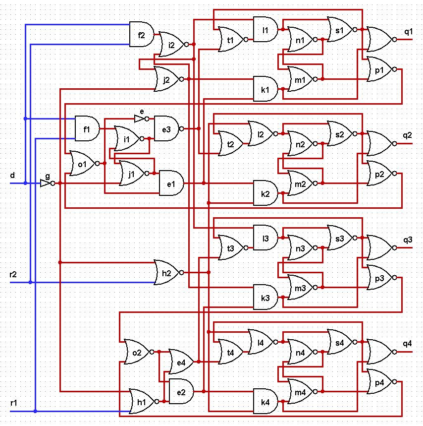
I do not have the opportunity to test the circuit in real embodiment. But if someone is interested in this, I will only welcome it. To make the initial setting, the input signal d must be set to 0. The internal signals m1, m2, m3, m4 must be set to 1. In order not to leave the two-input basis, this can be done for each of the elements m1, m2, m3, m4 as follows .
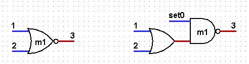
The element on the left is converted to the subschema on the right. The input signals r1, r2 can be set arbitrarily.
So, about the asynchronous descrambler. After reflection, I came to the conclusion that the only sane way for the synthesis of an asynchronous decoder is a phased doubling of the address using the add-on scheme over two decoders that is half the size of the address. Prove that there is no alternative way, I do not undertake. But I can say that the alternative path (if there is one) is much more expensive in terms of the number of added new signals.
In view of the foregoing, the discussion in this article will deal with a two-digit decoder. How to double the width of an asynchronous decoder, the topic of the next article.
')
So, we will describe the initial behavior of a two-bit asynchronous decoder. Oddly enough, it is not difficult to do in the language of STG, and the point here is not even a small bit.
Input Signals:
d - signal - command for address decryption operation;
r1, r2 - signals of bits of the register of the address.
Output signals:
q1 - switches if r1 = 1 and r2 = 1;
q2 - switches if r1 = 1 and r2 = 0;
q3 - switches if r1 = 0 and r2 = 1;
q4 - switches if r1 = 0 and r2 = 0.
The stepwise execution of the decryption operation is as follows:
0. When the signal d is 0, the external control circuit (MSC) randomly switches the signals r1 and r2. The decoder circuit (SD) does not track changes in the signals r1 and r2.
1. The MAS produces a d + signal, a command for the decryption operation. At this point, the MAS sets the signals r1 and r2 to a specific value. The MAS ensures that until the end of the decryption operation, the signals r1 and r2 will not change their value.
2. Depending on the value of the signals r1 and r2, the LED produces one of the signals: either q1 +, or q2 +, or q3 +, or q4 +.
3. The MAS produces a d- signal.
4. The LED produces one of the signals in accordance with clause 2: either q1-, or q2-, or q3-, or q4-. This signal is the signal for the end of the decryption operation. After that, the MAS can again change the signals r1 and r2 in an arbitrary manner.
A bit of discussion about how the two-bit asynchronous decoder circuit was synthesized. In fact, it consists of two, occurring in parallel, “level choices” (for each of the signals r1 and r2). Read more about the “level selection” here. Then alternative branches in two parallel processes are synchronized in pairs. The result is four alternative branches. In the above graph of the adjusted final behavior, only four alternative branches are visible. But this is a tribute to the STG language. It is not convenient to describe on it actually occurring processes. All the above “choices by level” and “synchronization of alternative branches” are encrypted in this behavior.
You can add that the synthesized behavior is not the result of some insights. This is the result of a targeted application of the methodology presented here. For each new signal, there is a rationale for adding it.
As a result, according to the presented graph of the final behavior, you can obtain logical functions for each signal:
; ; ; ;
; ; ; ;
; ; ; ;
; ; ; ;
; ; ; ;
; ; ; ;
; ; ; ;
; ; ; ;
; ; ; ;
; ; ; ;
; ; ; ;
; ; ; .
As you can see, all the equations are placed in the basis of 2-NOT, 2-OR-NOT.
But actually the SI itself is a two-bit asynchronous decoder circuit.
I do not have the opportunity to test the circuit in real embodiment. But if someone is interested in this, I will only welcome it. To make the initial setting, the input signal d must be set to 0. The internal signals m1, m2, m3, m4 must be set to 1. In order not to leave the two-input basis, this can be done for each of the elements m1, m2, m3, m4 as follows .
The element on the left is converted to the subschema on the right. The input signals r1, r2 can be set arbitrarily.
Source: https://habr.com/ru/post/335178/
All Articles