Is an asynchronous processor possible?
The quote from the comments to the previous article: “Unfortunately, the data, addresses and any operations on them are not suitable for graph representation. If you figure out how to do it, there will be a revolution. And without data, addresses, and arithmetic, the best that can be made asynchronous (using the graph method) is the Turing machine. But not a processor, for example. Therefore, the subject and abandoned, for 20 years as. "In the competence of the author can not be doubted, after all the doctor of science. But I'm trying to make a revolution.
As can be seen from the quotation, the problem consists of two parts: operations on data and operations on addresses. I will deal with addresses in the next article, and now - the data.
For example, I will try to make a register discharge circuit that performs two operations. Why two? Because two, three operations or ten - there is no fundamental difference. From an increase in the number of operations, only the amount of calculations increases during the synthesis of the circuit. The main thing that such operations were more than one. As operations I will choose copying from the buffer and addition with the contents of another register.
')
So, I will try to draw the behavior of the discharge of such a register. As I understand, the problem of describing the behavior of an object (information carrier) is that it interacts with other objects (information carriers). And these related objects can change their values arbitrarily (relative to the object being described). If there are 2, 3 or more related objects, then describing all possible changes to such objects in the STG language is meaningless. But there is a way out. It is enough to enter three new types of events in the STG:
f? - from this point on, the value of the signal f is not defined,
f / - from this point on the value of the signal f is determined, and it is equal to 1,
f \ - from this point on, the value of the signal f is determined, and it is 0.
The sequence of event types for a single signal is as follows:
after "+" - "-" or "?",
after "-" - "+" or "?",
after the "?" - "/" or "\",
after "/" - "?" or "-",
after "\" - "?" or "+".
Using new types of events you can describe the behavior of the register register.
Input Signals:
a - command for the operation of adding the value of the second register;
c - command for copying from buffer;
r0 is the value of the corresponding digit of the second register;
b is the value of the corresponding buffer level;
y0 is the transfer signal from the low-order digit during the addition operation;
n0 is the signal to refuse transfer from the low-order digit during the addition operation.
Output signals:
r - the value of the discharge register described;
t is the completion signal of the addition operation;
t0 - signal to complete the copy operation;
y is the signal for transfer to the high order during the addition operation;
n is the signal of failure to transfer to the high order during the addition operation.
The process of executing commands in steps looks like this:
Copy:
1. The external control circuit (MAS) produces a signal c +. At this point, the signal b is set in one of the states (0 or 1).
2. A register discharge circuit (CPP) generates a t0 + signal for a VUS.
3. VUS produces a signal c-.
4. If necessary, the CPP changes the value of the signal r to the opposite.
5. CPP generates a signal to complete the operation t0-. After that, the MAS can change the value of the signal b.
Addition:
1. MAS produces a + signal. At this point, the signal r0 is set in one of the states (0 or 1).
2. If this is possible without using information about the transfer from the low-order bit, the CPP produces a y + or n + signal for the high-order bit.
3. SRP waits from the lower order signal y0 + or n0 +.
4. produces a y + or n + signal for the most significant digit, if it has not yet been formed.
5. CPP generates a t + signal for the MAS.
6. MAS, collecting signals t + from all digits, produces a signal a-.
7. CPP produces a y- or n- signal for the most significant digit.
8. CPP waits for the signal y0- or n0- from the lower order.
9. If necessary, the CPP changes the value of the signal r to the opposite.
10. CPP generates a signal to complete the operation t-. After that, the MAS can change the value of the signal r0.
The interaction with the low order is carried out indirectly through the MAS. The introduction of a direct response signal for the lower order would allow paralleling the interaction with the MAS and with adjacent discharges. But for this article I decided to choose the original task easier.
It would seem that the task has been compiled; it is possible to proceed to the synthesis of the scheme. But not everything is so simple. None of the known methods is able to synthesize the SI scheme for this type of behavior (even if it adapts new types of events). Moreover, in my opinion, none of the methods will be able to cram this task into a more or less acceptable element base.
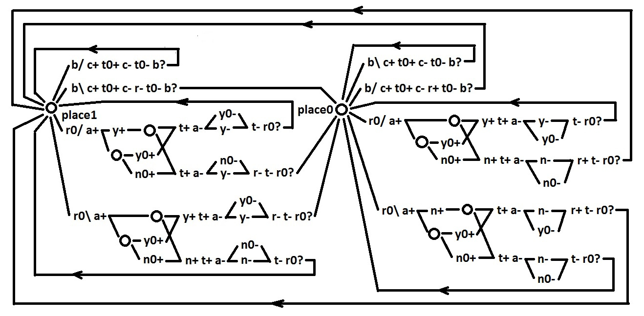
But, fortunately there is my method, which allows to solve these problems. I will not give here the process of updating the original task. I will show only the final result. For convenience, I will show it in four separate pictures.
Copy when r = 1.

Copy when r = 0.

Addition when r = 1.

Addition when r = 0.

And now the logical functions.

As you can see, the scheme was synthesized in basis 2-NOT, 2-OR-I did not set the task of limiting the loads on the outputs of the elements. But if each element output is limited to two loads, then the circuit will increase by 2–3 percent (in my estimation). But if you limit the inputs of the circuit to two loads, then this task is more complicated. Here I expect an increase in the scheme of interest by 25.
As can be seen from the quotation, the problem consists of two parts: operations on data and operations on addresses. I will deal with addresses in the next article, and now - the data.
For example, I will try to make a register discharge circuit that performs two operations. Why two? Because two, three operations or ten - there is no fundamental difference. From an increase in the number of operations, only the amount of calculations increases during the synthesis of the circuit. The main thing that such operations were more than one. As operations I will choose copying from the buffer and addition with the contents of another register.
')
So, I will try to draw the behavior of the discharge of such a register. As I understand, the problem of describing the behavior of an object (information carrier) is that it interacts with other objects (information carriers). And these related objects can change their values arbitrarily (relative to the object being described). If there are 2, 3 or more related objects, then describing all possible changes to such objects in the STG language is meaningless. But there is a way out. It is enough to enter three new types of events in the STG:
f? - from this point on, the value of the signal f is not defined,
f / - from this point on the value of the signal f is determined, and it is equal to 1,
f \ - from this point on, the value of the signal f is determined, and it is 0.
The sequence of event types for a single signal is as follows:
after "+" - "-" or "?",
after "-" - "+" or "?",
after the "?" - "/" or "\",
after "/" - "?" or "-",
after "\" - "?" or "+".
Using new types of events you can describe the behavior of the register register.
Input Signals:
a - command for the operation of adding the value of the second register;
c - command for copying from buffer;
r0 is the value of the corresponding digit of the second register;
b is the value of the corresponding buffer level;
y0 is the transfer signal from the low-order digit during the addition operation;
n0 is the signal to refuse transfer from the low-order digit during the addition operation.
Output signals:
r - the value of the discharge register described;
t is the completion signal of the addition operation;
t0 - signal to complete the copy operation;
y is the signal for transfer to the high order during the addition operation;
n is the signal of failure to transfer to the high order during the addition operation.
The process of executing commands in steps looks like this:
Copy:
1. The external control circuit (MAS) produces a signal c +. At this point, the signal b is set in one of the states (0 or 1).
2. A register discharge circuit (CPP) generates a t0 + signal for a VUS.
3. VUS produces a signal c-.
4. If necessary, the CPP changes the value of the signal r to the opposite.
5. CPP generates a signal to complete the operation t0-. After that, the MAS can change the value of the signal b.
Addition:
1. MAS produces a + signal. At this point, the signal r0 is set in one of the states (0 or 1).
2. If this is possible without using information about the transfer from the low-order bit, the CPP produces a y + or n + signal for the high-order bit.
3. SRP waits from the lower order signal y0 + or n0 +.
4. produces a y + or n + signal for the most significant digit, if it has not yet been formed.
5. CPP generates a t + signal for the MAS.
6. MAS, collecting signals t + from all digits, produces a signal a-.
7. CPP produces a y- or n- signal for the most significant digit.
8. CPP waits for the signal y0- or n0- from the lower order.
9. If necessary, the CPP changes the value of the signal r to the opposite.
10. CPP generates a signal to complete the operation t-. After that, the MAS can change the value of the signal r0.
The interaction with the low order is carried out indirectly through the MAS. The introduction of a direct response signal for the lower order would allow paralleling the interaction with the MAS and with adjacent discharges. But for this article I decided to choose the original task easier.
It would seem that the task has been compiled; it is possible to proceed to the synthesis of the scheme. But not everything is so simple. None of the known methods is able to synthesize the SI scheme for this type of behavior (even if it adapts new types of events). Moreover, in my opinion, none of the methods will be able to cram this task into a more or less acceptable element base.
But, fortunately there is my method, which allows to solve these problems. I will not give here the process of updating the original task. I will show only the final result. For convenience, I will show it in four separate pictures.
Copy when r = 1.
Copy when r = 0.
Addition when r = 1.
Addition when r = 0.
And now the logical functions.
As you can see, the scheme was synthesized in basis 2-NOT, 2-OR-I did not set the task of limiting the loads on the outputs of the elements. But if each element output is limited to two loads, then the circuit will increase by 2–3 percent (in my estimation). But if you limit the inputs of the circuit to two loads, then this task is more complicated. Here I expect an increase in the scheme of interest by 25.
Source: https://habr.com/ru/post/334030/
All Articles