Hybrid Memory Cube (HMC): what it is and how to connect it to FPGA

In the photo: The SKARAB platform for digital data processing from the MeerKAT telescope. Due to the HMC technology, each of the 64 telescope antennas can transmit data to the platform at a speed of 40 Gbps
Waiting for the new DDR5 SDRAM memory standard, which will appear next year, we are exploring alternative technologies. In this article, we examine the HMC memory (Hybrid Memory Cube), which provides a 15-fold increase in performance with 70% savings in power consumption per bit compared to DDR3 DRAM.
While DDR4 and DDR5 represent an evolution of the standard, HMC is a revolutionary technology that can change the market not only in the field of specialized high-performance computing, but also in consumer electronics, such as tablets and graphics cards, where form factor is important. energy efficiency and throughput.
HMC Architecture and Device
HMC - short for Hybrid Memory Cube - is a hybrid memory cube. Physically, the chip consists of several layers connected by silicon transitional ones using the TSV technology. The upper layers are DRAM-memory crystals, the lower layer is the controller that controls the transfer of data.
')
The internal structure of the HMC chip:
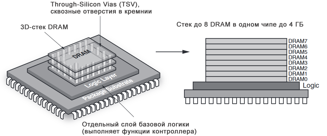
HMC is used where speed is needed, as well as a small number of chips for the required amount of memory. HMC chips can be combined into a consistent chain - up to 8 pieces. Chips are available in capacities of 2 and 4 GB. Data is transmitted via serial interfaces at a speed of 15 Gbit / s per line; total lines can be from 32 to 64. Thus, the theoretical bandwidth can reach 240 Gbit / s, but it is limited by the bandwidth of a DRAM chip at 160 Gbit / s.
The table below shows the consumption per bit of data:
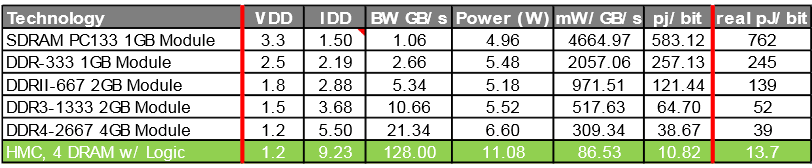
HMC Comparison Chart, DDR4 (first generation, 4 + 1 memory configuration)
In addition to the HMC, there are several similar directions from other development companies.
- Bandwidth Engine (BE) from MoSys - a chip designed to replace QDR-memory, works like SRAM. Uses serial transceivers at speeds up to 16 Gbps. The purpose of this type of memory is a low latency buffer for storing packet headers or look-up tables instead of storing whole packets.
- Ternary Content Addressable Memory (TCAM) - a special high-speed memory, used in routers and network switches, has a high price. High performance achieved due to high power consumption. Data transfer is carried out in parallel.
- High Bandwidth Memory (HBM) is a type of memory developed by Samsung. It is not available in the form of chips: if the user wants to use this memory, he must contact the company to make a silicon substrate for him and integrate it into the user's chip. This memory is similar to DDR and does not use serial transceivers for data transmission.
HMC connection examples
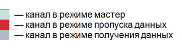
Physically, data is transmitted to the HMC sequentially over a SerDes interface at a speed of 15 Gbit / s. Soon there will be chips with a speed of 30 Gbit / s. 16 lines are combined into one logical channel. The channel can operate both in the full-channel mode and in the half-channel (8 lines are used). Usually HMCs are available with 2 or 4 channels. Each channel can be both master and intermediate. Intermediate modes are used when it is necessary to combine several chips in a chain. The processor must configure each HMC chip.
An example of combining HMC chips in a chain:

An example of combining HMC chips with a star, with the possibility of multi-host mode:

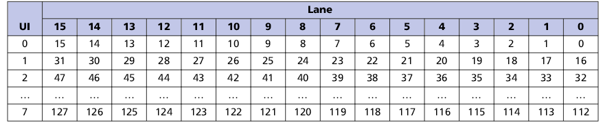
Transmission of data over a logical channel
Channel transfer structure:

Commands and data are transmitted in both directions using a packet protocol. Packages are made up of groups of 128 bits long, called FLIT. They are transmitted sequentially through the physical lines and then collected at the receiving side.
Three levels of package service:
- The physical layer provides reception, transmission, serialization and deserialization of data.
- The link layer provides low-level packet tracking.
- The transport layer determines the fields, packet headers, checks the integrity of the packets and the communication channel.
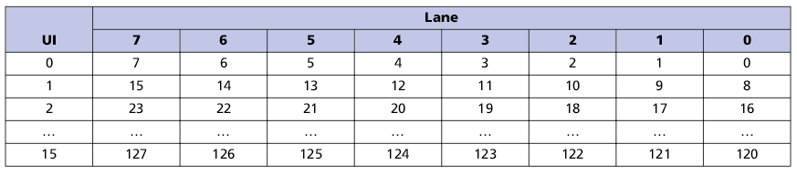
Organization of 128 bit FLIT transmission via physical lines in various modes:
1. Distribution of FLIT-package along the lines in full configuration (16 lines)
2. Distribution of FLIT-package lines in half configuration (8 lines)
Memory addressing
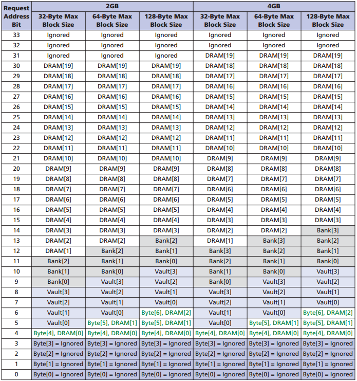
The packet header contains 34 address bits, including a bank, a DRAM address. The current configuration allows you to address a maximum of 4 GB for a single chip, with the upper 2 bits being ignored, they are reserved for the future. Reading and writing data occurs with 16-byte granulation. The block size can be set to 16, 32, 64, 128 bytes.
HMC Addressing:
More details on these commands can be found in the HMC specification on the Micron website.
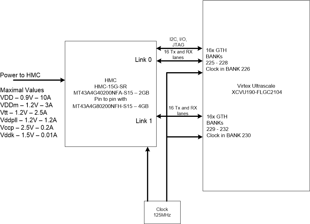
Typical HMC connection to Xilinx Virtex Ultrascale FPGA and power requirements
Memory is connected to the FPGA via GTX transceivers. You can use from 8 transceivers and up to 16 within one channel. There may be 4 such channels. To properly connect to FPGA transceivers, you need to follow a few rules:
- Transceivers within the channel must go in a row, it is not allowed to jump over the transceivers.
- For SSI (Stacked Silicon Interconnect) devices, the transceivers must be in the same SLR
- FPGA banks must go in a row, not allowed to jump through the banks
Typical connection to FPGA, two channels in full mode:
For a deeper study of this topic, you can go to the website of the consortium of developers of technology HMC - hybridmemorycube.org , where the latest HMC version 2.1 specification is published.
Source: https://habr.com/ru/post/333556/
All Articles