Multicore DSP TMS320C6678. Core memory organization
We continue a series of articles devoted to multi-core digital signal processors TMS320C6678. This article will discuss the kernel memory subsystem. The processor's memory architecture is one of the key points that directly affect its performance. Knowledge of the features of the organization of the memory architecture allows the developer to more efficiently use DSP resources. Modern processors have a rather complicated memory architecture, including several levels and cache controllers. In the case of DSP, working with memory is complicated by the freedom to choose the amount of cache memory at different levels, and for multicore processors there is a problem of synchronizing the cache of different cores.
TMS320C66x processors have a hierarchical 3-level memory architecture. The hierarchical memory architecture allows you to combine high speed memory and a large amount of available memory. In its development, the memory manufacturing technology lags somewhat behind processor technology. The clock frequency of the processor cores is increasing; requirements for the volume of internal and external memory are growing. At the same time, it is a difficult task to provide a processor with large-capacity memory operating at the core frequency. To solve this problem, hierarchical memory architectures in which memory is divided into several levels have been widely developed. A small memory works at the core frequency and represents the L1 level. Memory level L2 operates at a lower frequency, but has a larger volume. And so on. To speed up memory at lower levels (slow memory), fast memory can be partially or fully configured as cache memory.
The memory architecture of TMS320C66xx processors includes:
L1 and L2 memory can be fully or partially configured as a cache memory, speeding up work with slower L2 and L3 memory. The memory architecture plays one of the most important roles in overall processor performance, because it limits the bandwidth of the data feed channels to the actuators. Further details are considered on the components of the TMS320C66x processor memory architecture.
')
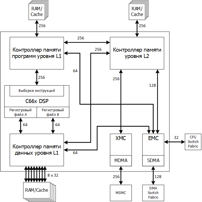
Figure 1 - CorePac core memory subsystem of the TMS320C66xx processor
The term CorePac stands for the single core of the TMS320C66x multi-core processor. The kernel is built in accordance with the structure presented in the following figure 1. It includes computing resources — 66 — discussed in the previous article and the following components related to the memory subsystem:
Below are the main aspects of the functioning of these devices.
Before embarking on the memory architecture of the TMS320C66x processor, it is advisable to get acquainted with the basic principles of the functioning of the cache.
The caching of programs and data has the main purpose of accelerating the work of a fast kernel with a slow large memory. Closest to the core operating at the core frequency is the L1 level memory, which has a small volume. Next comes the L2 memory of a larger volume, working, as a rule, twice as slowly. Then there can be a memory of the level L3, L4 and so on, having an even greater volume, but working even more slowly. This may be shared multi-core system memory or external memory chips.
The effectiveness of the use of the cache is based on two facts - the localization of programs and data in time and in memory space (temporal and spatial locality) [1]. Localization in time means repeated use of the same programs or data. Localization in memory space means that codes / data are used by groups. These two facts allow, when accessing a slow memory, to read from it the requested codes / data together with the neighboring groups of codes / data, to copy them into a faster memory, expecting that the future codes / data will already be present in the fast memory.
Groups of neighboring codes / data that are simultaneously copied to the cache are called cache line. Obviously, the larger the cache line size, the greater the efficiency of the cache in the spatial localization of codes / data, however, this complicates the cache architecture and leads to a reduction in the number of cache lines, that is, less uses the temporary code / data localization. The L1P cache line size is 32 bytes. Interestingly, codes executed from external memory in the TMS320C66x processor are always cached in L1P.
The simplest scheme for organizing caching is the direct-mapped cache. All main memory is divided into fragments, the size of each of which is equal to the size of the cache. Accordingly, the cache at a time can contain only one fragment of the main memory, or non-intersecting parts of several different fragments. Codes / data located in the main memory in different fragments, but in the lines corresponding to each other can not be simultaneously in the cache. There is a conflict conflict caching (conflict miss), which leads to the inefficiency of the cache. The main type of cache miss for this caching mechanism is a miss due to lack of cache capacity (capacity miss). Another inevitable cache inefficiency mode is initial caching (compulsory miss). This is a cache miss when you first access the main memory.
To get away from the problem of a lack of cache space in direct mapping caching mechanisms, so-called associative caches are used. We can assume that in them the direct mapping caching mechanism is simply duplicated (becomes two-variant - 2 way), expands 4 times (four-way - 4-way) and so on. Accordingly, the placement of codes / data from different fragments and intersecting by addresses becomes possible, and the more such intersecting codes / data can be simultaneously cached, the more options (paths - way) are supported. This architecture is more powerful than a cache with direct mapping, but at the cost of greater complexity and cost. All cache lines with overlapping addresses, that is, belonging to different paths, is called a set or a series of cache lines (Set). When one of the cache lines needs to be replaced, the path that has not been used for a long time is selected, compared to the others. This is followed by the LRU bit, which is part of the cache line. The structure of the cache opens the table.
The read-allocate cache cache is a type of cache in which the contents of the cache change only when the read fails, that is, when new data / codes are requested from the main memory and they are copied to the cache at the same time. When a write fails (when the kernel writes to a memory cell not mapped to the cache), the record goes directly to the main memory through a special write buffer (as part of the memory controller).
Caching with a delayed return of codes / data from the cache to the main memory (write back cache) means that when a record hits (write hit), the data / codes are not written to the main memory, but written only to the cache with a mark that the cache line is dirty (Dirty), that is, it must be copied to the main memory in the future.
When working with the cache on the DSP TMS320C66xx, the following aspects should be kept in mind. L2 memory is always cached in L1, you just need to configure L1 as a cache. When caching external memory, you must additionally specify what and where to cache. At the same time, codes from external memory in L1P are always cached. External memory is divided into 16 MB segments, and their cacheability is controlled by special MAR control registers.
Those fragments of memory that are allocated for the cache are not listed in the MEMORY section in the cmd-file.
When working with a cache, the problem of synchronization of the cache and the main memory (cache coherence) inevitably arises. Coherence (synchronization) cache means aligning the contents of the cache and the main memory. The problem of cache coherence always occurs when there is a shared memory resource, this memory is cacheable and the memory contents change. If the cache and main memory have different contents, that is, they are not synchronized, then one of the devices accessing the memory may access incorrect data.
The C66x processor provides automatic synchronization of data access by the core and EDMA / IDMA. When the DMA reads L2 SRAM, the data is read from the L1D cache and does not change in L2 SRAM. When DMA writes to L2 SRAM, data is written to both L2 SRAM and L1D. Automatic synchronization is based on the snooping mechanism. When accessed by the DMA, the caching of the codes / data in memory is automatically checked.
Manual synchronization (using special CSL commands) is necessary in the following cases:
A typical use of memory is the following situation. From the peripheral device 1, DMA writes the data to the array in the L2 memory for processing. Also through DMA, the processed data is output from L2 memory through peripheral device 2. To separate processing, data input and data output, two pairs of ping-pong buffers are used. When using only L2 memory with caching in L1, synchronization is performed automatically in the manner described above.
When 2 pairs of ping-pong buffers are placed in external memory and pass through 2 levels of cache — L2 and L1 — then manual synchronization is required. Before entering the next array into the input buffer via DMA channels, all L1D and L2 cache lines referring to this array must be declared invalidate. The array will be re-cached, causing the first access cache to overhead. Similarly, before the output array is sent through the DMA mechanism to the peripheral device, you must synchronize the L1D and L2 memory with the external memory - write back.
The performance of the cache memory is essential for the success of the entire processor. From this point of view, debugging tools for cache visualization are of particular importance. The cache visualization feature is supported by the code development environment for Texas Instruments Code Composer Studio processors in the processor's memory display window. It is necessary to additionally enable the function of memory analysis when displaying a window.
Program memory of the L1 (L1P) level is intended only for storing program codes. The memory capacity varies from device to device and is 32 KB for the TMS320C6678 processor. L1P memory can be partially configured as a cache. In this case, the cache size can be 0, 4, 8, 16 or 32 KB. The remaining memory is configured as normal RAM. Under the cache are allocated high addresses L1P. On power-up, the L1P memory is configured either completely as RAM, or with a maximum cache size (depending on the specific device).
L1P memory itself cannot be cached in other areas. L1P memory is written only via EDMA or IDMA channels. That is, writing to L1P memory is not available for a developer who wants to write something into it from the computational core during program execution.
Usually, when accessing L1P as RAM, the number of sleep cycles is 0, however, the maximum number of sleep cycles when working with L1P can reach 3. L1P memory management in cache mode is performed through a set of registers. Changing the size of the cache and other parameters can be carried out during the execution of the program.
We describe in more detail the operation of L1P in cache mode. In cache mode, L1P memory is a direct-mapped cache memory. This caching mechanism is the simplest and can most often lead to write cache conflicts from different sectors of the main memory. Obviously, it is believed that such a mechanism for program memory is sufficient, since program codes are characterized by the greatest degree of localization in memory space as compared with data.
Fix mode cache L1P (freeze mode) allows you to fix a snippet of code in the cache. Read hits are performed in the usual way, and cache misses do not change the contents of the cache and do not invalidate the codes in the cache. The L1P fix is useful when executing interrupts. Due to switching the processor state for a short time, there is no sense in “spoiling” the contents of the cache.
You can use global and block synchronization to synchronize L1P cache and main memory. Global implies the synchronization of the entire cache volume and is performed on significant events for the entire system, such as a task change, a change in the cache operation mode and others. Synchronization implies declaring the contents of the cache as invalidation and is performed by setting the bits in the control registers. In this case, the cache is not copied to the main memory, because the program cache is not modified by the kernel.
Block synchronization implies that in the cache control register, the starting address and the length of the code block are specified, which must be declared invalid.
Synchronization cache takes some time. Therefore, after synchronization initialization, it is advisable to wait for the end of synchronization. The end of synchronization is indicated by a flag in the control register. Accordingly, we need a code that analyzes this flag, and this code should not be located in a memory area dependent on the cache.
The L1P cache runs at the core frequency, and in the case of hits the cache there is no downtime, and the commands are executed in one clock cycle (in the pipeline). However, in the case of a cache miss, the situation is more complicated. L1P cache accesses L2 memory to fetch commands. The time to read a command is longer, but how much longer depends on the specific state of the pipeline and turns out to be difficult to predict. Often, pipeline downtime due to cache misses is hidden (does not affect the program execution process) due to the downtime of the command pipeline itself. On the TMS320C66x, the command pipeline is organized in such a way that its downtime overlaps with downtime due to cache misses, which makes it possible to get away from overstating the execution of the command execution process. Here, the idle time of the command pipeline is understood to mean that the sampling package in most cases contains more than one execution package, and the selection of commands is performed less frequently than their execution. The initial stages of the pipeline do not read the next command — idle until the subsequent stages of the pipeline run the current packages. Thus, there is additional time to access the memory level L2 and further, which allows partially or completely hide the L1P cache misses. This technology is referred to as pipelined handling of cache misses (L1P miss pipeline).
At C66x, an execution packet can be formed from two sampling packets.
However, it is obvious that for well-optimized codes, when the sampling packets almost coincide with the execution packets, this approach loses its effectiveness, and cache misses can significantly delay the execution of programs. Estimated values of execution delays due to cache misses for various pipeline status options can be found in the processor documentation.
Low power mode is used to reduce overall processor consumption in cases where it is of interest. L1P memory can be translated into a low consumption mode statically (static power-down), which implies setting the control bit of the low consumption mode; setting up an interrupt that wakes L1P and executing the IDLE command. Also, the memory can go into this mode dynamically (dynamic power-down), which means automatic transition when the program is executed from the SPLOOP buffer. Also, the L1P cache switches to low power mode (feature-oriented power-down) when the cache is inactive (disabled). That is, if L1P is configured as a cache, but not activated, then it is in a low power mode.
Reading L1P memory can be done by the kernel, DMA and IDMA. All commands include 2 protection bits - the user execution bit and the performance bit in the administrator mode. When reading kernel commands, they are always analyzed for the resolution of their execution in the current mode. If they are prohibited, an exception occurs (in the case of a read by the kernel) or an interrupt (in the case of a DMA / IDMA read). In addition, access to the L1P memory registers is also controlled by the L1P controller and causes an exception in the case of reading or writing a protected register.
DMA / IDMA read / write access is also monitored for resolution. You can configure different access rights to different pages of memory. L1P is built from 16 pages of memory protection.
The internal memory of the L1 data is up to 128 KB, depending on the processor model, and for the TMS320C6678 it is 32 KB of RAM. Part or all of the L1D can be configured as a cache.
L1D cache is a two-variant associative cache with read caching and delayed return caching (2-way set-associative, read-allocate, write back cache). The meanings of the listed concepts were explained above.
When enabled, L1D is initialized either completely as RAM or with a maximum cache size. Further configuration of the L1D is implemented through control registers.
The cache works as follows. The 32-bit address placed on the address bus has the structure illustrated in the figure.

Figure 2 - Address structure when accessing the cache
The offset field is an address within a single cache line. It is ignored by the cache controller, since the string is either in the cache or not entirely. A 64 byte line size corresponds to a 6 bit offset field. To establish the fact that there is a line in the cache, this field is not needed.
The set field specifies the set of rows to be accessed. The length of the set field depends on the size of the cache and lies within 5-14 bits.
The Tag field finally defines the address of the line being accessed, taking into account the required path (way).
The data cache, unlike program memory, can be changed by the processor core. Therefore, the return of changed data from the cache to the main memory (write back) occurs either by a kernel command, or simply automatically when replacing the cache line with a new line from the main memory. The size of the L1D cache may change dynamically.
In the commit mode, the L1D cache operates normally in the case of read and write hits and in the case of write miss. Only the LRU bit does not change when it misses. In case of a miss reading, the cache update does not occur. Cache sync commands continue to work as usual. The transition to the cache fixing mode and back is done by writing to the registers and can be done dynamically and quickly enough. In addition, L1D and L1P are often transferred to the commit mode at the same time. For this, in the control registers the bits are set sequentially.
Software synchronization L1D-cache is based on the implementation of three commands:
Synchronization can be global and block, similar to L1P memory. Unlike L1P, declaring the contents of L1D memory as invalid can lead to data loss (since it can be changed by the kernel), so in practice it is better to use either a block write write-invalidate operation or L2 cache synchronization commands.
In order for the L1D cache to be synchronized with L2 memory, modified by DMA, the L1D cache controller is able to process synchronization commands from L2. L2 generates read / write synchronization commands (snoop-read and snoop-write) only in response to the corresponding DMA controller activity. The snoop-read command comes from L2 when L2 understands that the requested DMA line is in the cache and is marked as modified (Dirty). L1D outputs this string to L2. The snoop-write command is formed when L2 realizes that the string generated by the DMA is written to the L1D cache. It does not matter if the string changed in L1D or not, it is overwritten by the new value.
To reduce the number of L1D accesses from the L2 side for the purpose of synchronization, L2 stores its own (shadow) copy of the L1D cache memory tags. This copy is updated each time L1D accesses L2 and is used for L2 to access it, and not L1D itself, in order to find out the state of certain cache lines. If a copy of the tags tells L2 that the replacement in L1D should be done, only then there is an appeal to L1D itself.
Let's take a closer look at the memory structure of the L1D. There are 8 banks of memory. Each bank has a width of one word - 4 bytes. Banks - single-port, that is, to one bank is possible only one appeal per clock. Two simultaneous calls to the same bank in different areas of the memory space cause a simple one clock cycle. If two calls go to the same word in the same bank, then there may be no downtime if these are two readings of any bytes in the word; if these are two records of different bytes in the word. If access comes from the core and DMA, then it will still be simple - one of the devices will be idle depending on the priority setting. If reads and writes are addressed to the same word in one bank, it will be easy, even if the bytes are different. L1D RAM and cache use the same memory structure.
L1D memory may be two accesses per clock. If there are no misses or no memory bank conflicts, then the call is executed in one clock cycle. In the case of L1D slip, data is extracted from L2, and if they are not present in L2, then from L3. If in one clock cycle there are 2 accesses to a single cache line that is not in the cache, then a miss results in only one clock cycle. Similarly, if two accesses to the same cache line occur sequentially, then it will be simple only for the first slip.
When replacing the old cache line with the new content is returned to the main memory through a special buffer (victim buffer). So that the replacement of rows does not cause additional downtime, old data is copied to the buffer, and reading of new data continues, and old data is returned to main memory in the background. Subsequent cache misses, however, must wait for the data return process to complete. If the misses do not conflict with each other, they are realized by pipeline and additional downtime does not occur. This concerns cache misses when reading. Misses of recording can cause downtime only under certain circumstances. Data that requires writing to L2 forms a queue in the write buffer (L1D write buffer).
L1D implements a memory architecture in which cache entry misses cause a lower level (L2) memory direct access without placing this data in the cache. A write buffer is used for this purpose. This buffer has a size of 128 bits and is 4-port, providing the ability to carry up to 4 separate data records in L2 simultaneously. Write misses cause downtime only if the write buffer is full. Also, the full write buffer may indirectly increase the idle time for a read miss. The point is that read slips are not serviced until the write buffer is completely free. This is necessary, since data can be read from the same address that is being written to, and the record must be completed before reading begins, otherwise incorrect data may be read.
Memory L2 operates at a frequency two times smaller than the frequency L1. It processes requests from the write buffer on its own frequency. In addition, possible conflicts between memory banks should be considered. You should try to have data from different memory banks in the write buffer to read them simultaneously and reduce possible downtime.Two subsequent miss records are combined into one and are executed simultaneously under certain conditions, in particular, the data must be located within adjacent 128 bits, both calls must go to L2 RAM (not the cache) and a number of others. These conditions occur when a large sequence of records in memory or when writing a small amount of data in a given structure in memory. The described mechanism reduces processor idle time during write failures and improves the overall performance of the L2 memory. It is essential for programs with a large number of cache entry errors.
As well as for L1P memory, to reduce total downtime for cache misses, pipelining of read misses is organized.
L1D- L1P. L1D , (idle mode). IDLE , ( ) . , L1D, L1P L2 DMA (PDC) «» , DMA . . .
To protect L1D memory, L1D memory accesses are checked for access in user / administrator mode and whether access to this memory area is allowed for this mode. If a call is made to unresolved addresses, an exception occurs. All hits from the side of the master devices (first of all, DSP and IDMA) are checked and the type of exclusion differs for internal and external calls. In addition to data access, cache synchronization operations are also subject to verification. Manual synchronization of the cache is allowed for both the administrator and user modes, however, in the user mode, the global declaring of data is invalidated and the cache size cannot be changed. Memory protection management is implemented using a set of registers.
L2 64 — 4096 TMS320C6678 512 . L2 1 256 . L2 , 4 . 128- . L2 L1D, L1P IDMA .
L2 . .
L2 cache is a 4-way associative cache. Unlike L1 Cache, L2 Cache is a cache with read and write caching. The memory address includes 3 fields - offset (offset), set (set) and tag (tag). The offset addresses a specific byte within a single cache line. L2-cache lines are 128-byte, so 7 bits are allocated on the offset field. The Set field sets the line number. The Tag field indicates which variant (Way) the given string belongs to and indicates the set of attributes, for example, valid data or not, and so on.
L1. L2- . L1- L2 - , L2- . DSP. XMC.
L2 . , , .
The resizing of the L2 cache can be made on the fly by programmatically writing the required flags to the control registers. In this case, you must be careful with the synchronization of the cache. The CorePac Core Guide provides the required sequence of actions.
The commit cache mode is supported, similar to L1 memory.
It is also possible to force software synchronization L2 cache. Similar to L1, it can be global and block. Some synchronization commands affect simultaneously the operation of L1 memory.
, . (MAR). . , . , . MAR . , [2].
L1P L1D L2, L2 ( ), L2 MAR- . , « » – L2 L1D ( ). DSP , . L1P , , MAR-.
L1 L2. L2 L1D-. L2 L1P, ( ) - L2 L1.
L1 L2 – snoop-. Snoop-read – – L2, DMA L2 , L1D , L1 L2 , . L2 L1D- , ( , LRU ). Snoop-write – – L2 L2 DMA , L1D-. , , . 256 L2 L1D. .
L2- «» , L1D ( L1P) .
L1 L3 ( L2 ) – victim writebacks – L2 , L2-, , L2-.
XMC L2- MAR.
L2 memory is placed in reduced consumption mode statically or dynamically. Dynamically - for short periods of time. Statically - for a longer time when the processor (CorePac core) is in standby mode. A static transition to low consumption mode occurs with the transition of the entire kernel to sleep mode. If during sleep DMA accesses L1PD or L2 memory, then all three memory controllers wake up, and after processing the request, the DMA lower consumption controller (PDC) puts them to sleep again.
L2 . L2 Retenion Until Access – RTA. «» , . , L2 , .
L2, L1, , . . [2].
DMA – IDMA – , L1P, L1D L2, (CFG). 2 . – L1 L2-. IDMA L1 L2- , . – IDMA CFG-. IDMA .
IDMA 2 . 0 (channel 0) – CFG. 1 (channel 1) . IDMA DMA- DSP- . [2].
EMC CorePac . , , .
EMC 2 – CFG DMA «» — Slave DMA – SDMA. SDMA , , DMA ( ), SRIO , . , , .
XMC 4 :
CorePac MSM.
( ) MSM RAM EMIF CorePac.
MPAX. , .
The TMS320C66x processor supports regular 32-bit internal memory addressing. This length of the address allows you to access the 4 GB address space. At the same time, modern multi-core data processing systems require large amounts of addressable memory. To expand the possibilities of working with large amounts of memory, the processor is able to expand the internal 32-bit CorePac addresses to 36-bit. 36-bit addressing allows you to address up to 64 GB of memory.
32- 16 , , , MSM. .
XMC . MPAX, XMC .
MPAX . 16 MPAX 3.

3 — MPAX
BADDR SEGSZ . 4 4 . . 36- , , , ( ) . , , .
[2]. , , , , .
:
Literature:
Content
- Introduction
- Cache Principles
- Local memory of L1P programs
- L1D local data memory
- Local memory L2
- Internal Direct Memory Access Controller - IDMA
- External Memory Access Controller
- Memory expansion controller
Introduction
TMS320C66x processors have a hierarchical 3-level memory architecture. The hierarchical memory architecture allows you to combine high speed memory and a large amount of available memory. In its development, the memory manufacturing technology lags somewhat behind processor technology. The clock frequency of the processor cores is increasing; requirements for the volume of internal and external memory are growing. At the same time, it is a difficult task to provide a processor with large-capacity memory operating at the core frequency. To solve this problem, hierarchical memory architectures in which memory is divided into several levels have been widely developed. A small memory works at the core frequency and represents the L1 level. Memory level L2 operates at a lower frequency, but has a larger volume. And so on. To speed up memory at lower levels (slow memory), fast memory can be partially or fully configured as cache memory.
The memory architecture of TMS320C66xx processors includes:
- L1P internal local program memory and L1D data memory operating at core frequency;
- L2 internal local memory shared by programs and data;
- MSM (Multicore Shared Memory) internal shared memory for all cores, which can be configured as L2 or L3 memory;
- interface external memory level L3.
L1 and L2 memory can be fully or partially configured as a cache memory, speeding up work with slower L2 and L3 memory. The memory architecture plays one of the most important roles in overall processor performance, because it limits the bandwidth of the data feed channels to the actuators. Further details are considered on the components of the TMS320C66x processor memory architecture.
')
Figure 1 - CorePac core memory subsystem of the TMS320C66xx processor
The term CorePac stands for the single core of the TMS320C66x multi-core processor. The kernel is built in accordance with the structure presented in the following figure 1. It includes computing resources — 66 — discussed in the previous article and the following components related to the memory subsystem:
- L1 (L1P) program memory controller;
- data memory controller L1 (L1D);
- memory controller level L2 (L2);
- Internal Direct Memory Access (IDMA) controller
- external memory access controller (EMC);
- memory expansion controller (XMC);
Below are the main aspects of the functioning of these devices.
Cache Principles
Before embarking on the memory architecture of the TMS320C66x processor, it is advisable to get acquainted with the basic principles of the functioning of the cache.
The caching of programs and data has the main purpose of accelerating the work of a fast kernel with a slow large memory. Closest to the core operating at the core frequency is the L1 level memory, which has a small volume. Next comes the L2 memory of a larger volume, working, as a rule, twice as slowly. Then there can be a memory of the level L3, L4 and so on, having an even greater volume, but working even more slowly. This may be shared multi-core system memory or external memory chips.
The effectiveness of the use of the cache is based on two facts - the localization of programs and data in time and in memory space (temporal and spatial locality) [1]. Localization in time means repeated use of the same programs or data. Localization in memory space means that codes / data are used by groups. These two facts allow, when accessing a slow memory, to read from it the requested codes / data together with the neighboring groups of codes / data, to copy them into a faster memory, expecting that the future codes / data will already be present in the fast memory.
Groups of neighboring codes / data that are simultaneously copied to the cache are called cache line. Obviously, the larger the cache line size, the greater the efficiency of the cache in the spatial localization of codes / data, however, this complicates the cache architecture and leads to a reduction in the number of cache lines, that is, less uses the temporary code / data localization. The L1P cache line size is 32 bytes. Interestingly, codes executed from external memory in the TMS320C66x processor are always cached in L1P.
The simplest scheme for organizing caching is the direct-mapped cache. All main memory is divided into fragments, the size of each of which is equal to the size of the cache. Accordingly, the cache at a time can contain only one fragment of the main memory, or non-intersecting parts of several different fragments. Codes / data located in the main memory in different fragments, but in the lines corresponding to each other can not be simultaneously in the cache. There is a conflict conflict caching (conflict miss), which leads to the inefficiency of the cache. The main type of cache miss for this caching mechanism is a miss due to lack of cache capacity (capacity miss). Another inevitable cache inefficiency mode is initial caching (compulsory miss). This is a cache miss when you first access the main memory.
To get away from the problem of a lack of cache space in direct mapping caching mechanisms, so-called associative caches are used. We can assume that in them the direct mapping caching mechanism is simply duplicated (becomes two-variant - 2 way), expands 4 times (four-way - 4-way) and so on. Accordingly, the placement of codes / data from different fragments and intersecting by addresses becomes possible, and the more such intersecting codes / data can be simultaneously cached, the more options (paths - way) are supported. This architecture is more powerful than a cache with direct mapping, but at the cost of greater complexity and cost. All cache lines with overlapping addresses, that is, belonging to different paths, is called a set or a series of cache lines (Set). When one of the cache lines needs to be replaced, the path that has not been used for a long time is selected, compared to the others. This is followed by the LRU bit, which is part of the cache line. The structure of the cache opens the table.
| way1 | way2 | |
|---|---|---|
| set1 | line0 | line0 |
| set2 | line1 | line1 |
| set3 | line2 | line2 |
The read-allocate cache cache is a type of cache in which the contents of the cache change only when the read fails, that is, when new data / codes are requested from the main memory and they are copied to the cache at the same time. When a write fails (when the kernel writes to a memory cell not mapped to the cache), the record goes directly to the main memory through a special write buffer (as part of the memory controller).
Caching with a delayed return of codes / data from the cache to the main memory (write back cache) means that when a record hits (write hit), the data / codes are not written to the main memory, but written only to the cache with a mark that the cache line is dirty (Dirty), that is, it must be copied to the main memory in the future.
When working with the cache on the DSP TMS320C66xx, the following aspects should be kept in mind. L2 memory is always cached in L1, you just need to configure L1 as a cache. When caching external memory, you must additionally specify what and where to cache. At the same time, codes from external memory in L1P are always cached. External memory is divided into 16 MB segments, and their cacheability is controlled by special MAR control registers.
Those fragments of memory that are allocated for the cache are not listed in the MEMORY section in the cmd-file.
When working with a cache, the problem of synchronization of the cache and the main memory (cache coherence) inevitably arises. Coherence (synchronization) cache means aligning the contents of the cache and the main memory. The problem of cache coherence always occurs when there is a shared memory resource, this memory is cacheable and the memory contents change. If the cache and main memory have different contents, that is, they are not synchronized, then one of the devices accessing the memory may access incorrect data.
The C66x processor provides automatic synchronization of data access by the core and EDMA / IDMA. When the DMA reads L2 SRAM, the data is read from the L1D cache and does not change in L2 SRAM. When DMA writes to L2 SRAM, data is written to both L2 SRAM and L1D. Automatic synchronization is based on the snooping mechanism. When accessed by the DMA, the caching of the codes / data in memory is automatically checked.
Manual synchronization (using special CSL commands) is necessary in the following cases:
- data or code is written to external memory via DMA or from another external source, which is then read by the CPU;
- The CPU writes data to external memory, from where they are then taken by a DMA or other device;
- DMA writes codes in L2 SRAM, which are then executed by the CPU;
- the kernel writes code in L2 SRAM or external memory, and then it executes them.
A typical use of memory is the following situation. From the peripheral device 1, DMA writes the data to the array in the L2 memory for processing. Also through DMA, the processed data is output from L2 memory through peripheral device 2. To separate processing, data input and data output, two pairs of ping-pong buffers are used. When using only L2 memory with caching in L1, synchronization is performed automatically in the manner described above.
When 2 pairs of ping-pong buffers are placed in external memory and pass through 2 levels of cache — L2 and L1 — then manual synchronization is required. Before entering the next array into the input buffer via DMA channels, all L1D and L2 cache lines referring to this array must be declared invalidate. The array will be re-cached, causing the first access cache to overhead. Similarly, before the output array is sent through the DMA mechanism to the peripheral device, you must synchronize the L1D and L2 memory with the external memory - write back.
The performance of the cache memory is essential for the success of the entire processor. From this point of view, debugging tools for cache visualization are of particular importance. The cache visualization feature is supported by the code development environment for Texas Instruments Code Composer Studio processors in the processor's memory display window. It is necessary to additionally enable the function of memory analysis when displaying a window.
Local memory of L1P programs
Program memory of the L1 (L1P) level is intended only for storing program codes. The memory capacity varies from device to device and is 32 KB for the TMS320C6678 processor. L1P memory can be partially configured as a cache. In this case, the cache size can be 0, 4, 8, 16 or 32 KB. The remaining memory is configured as normal RAM. Under the cache are allocated high addresses L1P. On power-up, the L1P memory is configured either completely as RAM, or with a maximum cache size (depending on the specific device).
L1P memory itself cannot be cached in other areas. L1P memory is written only via EDMA or IDMA channels. That is, writing to L1P memory is not available for a developer who wants to write something into it from the computational core during program execution.
Usually, when accessing L1P as RAM, the number of sleep cycles is 0, however, the maximum number of sleep cycles when working with L1P can reach 3. L1P memory management in cache mode is performed through a set of registers. Changing the size of the cache and other parameters can be carried out during the execution of the program.
We describe in more detail the operation of L1P in cache mode. In cache mode, L1P memory is a direct-mapped cache memory. This caching mechanism is the simplest and can most often lead to write cache conflicts from different sectors of the main memory. Obviously, it is believed that such a mechanism for program memory is sufficient, since program codes are characterized by the greatest degree of localization in memory space as compared with data.
Fix mode cache L1P (freeze mode) allows you to fix a snippet of code in the cache. Read hits are performed in the usual way, and cache misses do not change the contents of the cache and do not invalidate the codes in the cache. The L1P fix is useful when executing interrupts. Due to switching the processor state for a short time, there is no sense in “spoiling” the contents of the cache.
You can use global and block synchronization to synchronize L1P cache and main memory. Global implies the synchronization of the entire cache volume and is performed on significant events for the entire system, such as a task change, a change in the cache operation mode and others. Synchronization implies declaring the contents of the cache as invalidation and is performed by setting the bits in the control registers. In this case, the cache is not copied to the main memory, because the program cache is not modified by the kernel.
Block synchronization implies that in the cache control register, the starting address and the length of the code block are specified, which must be declared invalid.
Synchronization cache takes some time. Therefore, after synchronization initialization, it is advisable to wait for the end of synchronization. The end of synchronization is indicated by a flag in the control register. Accordingly, we need a code that analyzes this flag, and this code should not be located in a memory area dependent on the cache.
The L1P cache runs at the core frequency, and in the case of hits the cache there is no downtime, and the commands are executed in one clock cycle (in the pipeline). However, in the case of a cache miss, the situation is more complicated. L1P cache accesses L2 memory to fetch commands. The time to read a command is longer, but how much longer depends on the specific state of the pipeline and turns out to be difficult to predict. Often, pipeline downtime due to cache misses is hidden (does not affect the program execution process) due to the downtime of the command pipeline itself. On the TMS320C66x, the command pipeline is organized in such a way that its downtime overlaps with downtime due to cache misses, which makes it possible to get away from overstating the execution of the command execution process. Here, the idle time of the command pipeline is understood to mean that the sampling package in most cases contains more than one execution package, and the selection of commands is performed less frequently than their execution. The initial stages of the pipeline do not read the next command — idle until the subsequent stages of the pipeline run the current packages. Thus, there is additional time to access the memory level L2 and further, which allows partially or completely hide the L1P cache misses. This technology is referred to as pipelined handling of cache misses (L1P miss pipeline).
At C66x, an execution packet can be formed from two sampling packets.
However, it is obvious that for well-optimized codes, when the sampling packets almost coincide with the execution packets, this approach loses its effectiveness, and cache misses can significantly delay the execution of programs. Estimated values of execution delays due to cache misses for various pipeline status options can be found in the processor documentation.
Low power mode is used to reduce overall processor consumption in cases where it is of interest. L1P memory can be translated into a low consumption mode statically (static power-down), which implies setting the control bit of the low consumption mode; setting up an interrupt that wakes L1P and executing the IDLE command. Also, the memory can go into this mode dynamically (dynamic power-down), which means automatic transition when the program is executed from the SPLOOP buffer. Also, the L1P cache switches to low power mode (feature-oriented power-down) when the cache is inactive (disabled). That is, if L1P is configured as a cache, but not activated, then it is in a low power mode.
Reading L1P memory can be done by the kernel, DMA and IDMA. All commands include 2 protection bits - the user execution bit and the performance bit in the administrator mode. When reading kernel commands, they are always analyzed for the resolution of their execution in the current mode. If they are prohibited, an exception occurs (in the case of a read by the kernel) or an interrupt (in the case of a DMA / IDMA read). In addition, access to the L1P memory registers is also controlled by the L1P controller and causes an exception in the case of reading or writing a protected register.
DMA / IDMA read / write access is also monitored for resolution. You can configure different access rights to different pages of memory. L1P is built from 16 pages of memory protection.
L1D local data memory
The internal memory of the L1 data is up to 128 KB, depending on the processor model, and for the TMS320C6678 it is 32 KB of RAM. Part or all of the L1D can be configured as a cache.
L1D cache is a two-variant associative cache with read caching and delayed return caching (2-way set-associative, read-allocate, write back cache). The meanings of the listed concepts were explained above.
When enabled, L1D is initialized either completely as RAM or with a maximum cache size. Further configuration of the L1D is implemented through control registers.
The cache works as follows. The 32-bit address placed on the address bus has the structure illustrated in the figure.
Figure 2 - Address structure when accessing the cache
The offset field is an address within a single cache line. It is ignored by the cache controller, since the string is either in the cache or not entirely. A 64 byte line size corresponds to a 6 bit offset field. To establish the fact that there is a line in the cache, this field is not needed.
The set field specifies the set of rows to be accessed. The length of the set field depends on the size of the cache and lies within 5-14 bits.
The Tag field finally defines the address of the line being accessed, taking into account the required path (way).
The data cache, unlike program memory, can be changed by the processor core. Therefore, the return of changed data from the cache to the main memory (write back) occurs either by a kernel command, or simply automatically when replacing the cache line with a new line from the main memory. The size of the L1D cache may change dynamically.
In the commit mode, the L1D cache operates normally in the case of read and write hits and in the case of write miss. Only the LRU bit does not change when it misses. In case of a miss reading, the cache update does not occur. Cache sync commands continue to work as usual. The transition to the cache fixing mode and back is done by writing to the registers and can be done dynamically and quickly enough. In addition, L1D and L1P are often transferred to the commit mode at the same time. For this, in the control registers the bits are set sequentially.
Software synchronization L1D-cache is based on the implementation of three commands:
- declaring data invalid;
- data return to main memory (writeback);
- both operations at the same time (writeback-invalidation).
Synchronization can be global and block, similar to L1P memory. Unlike L1P, declaring the contents of L1D memory as invalid can lead to data loss (since it can be changed by the kernel), so in practice it is better to use either a block write write-invalidate operation or L2 cache synchronization commands.
In order for the L1D cache to be synchronized with L2 memory, modified by DMA, the L1D cache controller is able to process synchronization commands from L2. L2 generates read / write synchronization commands (snoop-read and snoop-write) only in response to the corresponding DMA controller activity. The snoop-read command comes from L2 when L2 understands that the requested DMA line is in the cache and is marked as modified (Dirty). L1D outputs this string to L2. The snoop-write command is formed when L2 realizes that the string generated by the DMA is written to the L1D cache. It does not matter if the string changed in L1D or not, it is overwritten by the new value.
To reduce the number of L1D accesses from the L2 side for the purpose of synchronization, L2 stores its own (shadow) copy of the L1D cache memory tags. This copy is updated each time L1D accesses L2 and is used for L2 to access it, and not L1D itself, in order to find out the state of certain cache lines. If a copy of the tags tells L2 that the replacement in L1D should be done, only then there is an appeal to L1D itself.
Let's take a closer look at the memory structure of the L1D. There are 8 banks of memory. Each bank has a width of one word - 4 bytes. Banks - single-port, that is, to one bank is possible only one appeal per clock. Two simultaneous calls to the same bank in different areas of the memory space cause a simple one clock cycle. If two calls go to the same word in the same bank, then there may be no downtime if these are two readings of any bytes in the word; if these are two records of different bytes in the word. If access comes from the core and DMA, then it will still be simple - one of the devices will be idle depending on the priority setting. If reads and writes are addressed to the same word in one bank, it will be easy, even if the bytes are different. L1D RAM and cache use the same memory structure.
L1D memory may be two accesses per clock. If there are no misses or no memory bank conflicts, then the call is executed in one clock cycle. In the case of L1D slip, data is extracted from L2, and if they are not present in L2, then from L3. If in one clock cycle there are 2 accesses to a single cache line that is not in the cache, then a miss results in only one clock cycle. Similarly, if two accesses to the same cache line occur sequentially, then it will be simple only for the first slip.
When replacing the old cache line with the new content is returned to the main memory through a special buffer (victim buffer). So that the replacement of rows does not cause additional downtime, old data is copied to the buffer, and reading of new data continues, and old data is returned to main memory in the background. Subsequent cache misses, however, must wait for the data return process to complete. If the misses do not conflict with each other, they are realized by pipeline and additional downtime does not occur. This concerns cache misses when reading. Misses of recording can cause downtime only under certain circumstances. Data that requires writing to L2 forms a queue in the write buffer (L1D write buffer).
L1D implements a memory architecture in which cache entry misses cause a lower level (L2) memory direct access without placing this data in the cache. A write buffer is used for this purpose. This buffer has a size of 128 bits and is 4-port, providing the ability to carry up to 4 separate data records in L2 simultaneously. Write misses cause downtime only if the write buffer is full. Also, the full write buffer may indirectly increase the idle time for a read miss. The point is that read slips are not serviced until the write buffer is completely free. This is necessary, since data can be read from the same address that is being written to, and the record must be completed before reading begins, otherwise incorrect data may be read.
Memory L2 operates at a frequency two times smaller than the frequency L1. It processes requests from the write buffer on its own frequency. In addition, possible conflicts between memory banks should be considered. You should try to have data from different memory banks in the write buffer to read them simultaneously and reduce possible downtime.Two subsequent miss records are combined into one and are executed simultaneously under certain conditions, in particular, the data must be located within adjacent 128 bits, both calls must go to L2 RAM (not the cache) and a number of others. These conditions occur when a large sequence of records in memory or when writing a small amount of data in a given structure in memory. The described mechanism reduces processor idle time during write failures and improves the overall performance of the L2 memory. It is essential for programs with a large number of cache entry errors.
As well as for L1P memory, to reduce total downtime for cache misses, pipelining of read misses is organized.
L1D- L1P. L1D , (idle mode). IDLE , ( ) . , L1D, L1P L2 DMA (PDC) «» , DMA . . .
To protect L1D memory, L1D memory accesses are checked for access in user / administrator mode and whether access to this memory area is allowed for this mode. If a call is made to unresolved addresses, an exception occurs. All hits from the side of the master devices (first of all, DSP and IDMA) are checked and the type of exclusion differs for internal and external calls. In addition to data access, cache synchronization operations are also subject to verification. Manual synchronization of the cache is allowed for both the administrator and user modes, however, in the user mode, the global declaring of data is invalidated and the cache size cannot be changed. Memory protection management is implemented using a set of registers.
Local memory L2
L2 64 — 4096 TMS320C6678 512 . L2 1 256 . L2 , 4 . 128- . L2 L1D, L1P IDMA .
L2 . .
L2 cache is a 4-way associative cache. Unlike L1 Cache, L2 Cache is a cache with read and write caching. The memory address includes 3 fields - offset (offset), set (set) and tag (tag). The offset addresses a specific byte within a single cache line. L2-cache lines are 128-byte, so 7 bits are allocated on the offset field. The Set field sets the line number. The Tag field indicates which variant (Way) the given string belongs to and indicates the set of attributes, for example, valid data or not, and so on.
L1. L2- . L1- L2 - , L2- . DSP. XMC.
L2 . , , .
The resizing of the L2 cache can be made on the fly by programmatically writing the required flags to the control registers. In this case, you must be careful with the synchronization of the cache. The CorePac Core Guide provides the required sequence of actions.
The commit cache mode is supported, similar to L1 memory.
It is also possible to force software synchronization L2 cache. Similar to L1, it can be global and block. Some synchronization commands affect simultaneously the operation of L1 memory.
, . (MAR). . , . , . MAR . , [2].
L1P L1D L2, L2 ( ), L2 MAR- . , « » – L2 L1D ( ). DSP , . L1P , , MAR-.
L1 L2. L2 L1D-. L2 L1P, ( ) - L2 L1.
L1 L2 – snoop-. Snoop-read – – L2, DMA L2 , L1D , L1 L2 , . L2 L1D- , ( , LRU ). Snoop-write – – L2 L2 DMA , L1D-. , , . 256 L2 L1D. .
L2- «» , L1D ( L1P) .
L1 L3 ( L2 ) – victim writebacks – L2 , L2-, , L2-.
XMC L2- MAR.
L2 memory is placed in reduced consumption mode statically or dynamically. Dynamically - for short periods of time. Statically - for a longer time when the processor (CorePac core) is in standby mode. A static transition to low consumption mode occurs with the transition of the entire kernel to sleep mode. If during sleep DMA accesses L1PD or L2 memory, then all three memory controllers wake up, and after processing the request, the DMA lower consumption controller (PDC) puts them to sleep again.
L2 . L2 Retenion Until Access – RTA. «» , . , L2 , .
L2, L1, , . . [2].
— IDMA
DMA – IDMA – , L1P, L1D L2, (CFG). 2 . – L1 L2-. IDMA L1 L2- , . – IDMA CFG-. IDMA .
IDMA 2 . 0 (channel 0) – CFG. 1 (channel 1) . IDMA DMA- DSP- . [2].
— EMC
EMC CorePac . , , .
EMC 2 – CFG DMA «» — Slave DMA – SDMA. SDMA , , DMA ( ), SRIO , . , , .
— XMC
XMC 4 :
- MSMC – MDMA- L2- MSM-;
- , CorePac;
- ;
- (prefetching).
CorePac MSM.
( ) MSM RAM EMIF CorePac.
MPAX. , .
The TMS320C66x processor supports regular 32-bit internal memory addressing. This length of the address allows you to access the 4 GB address space. At the same time, modern multi-core data processing systems require large amounts of addressable memory. To expand the possibilities of working with large amounts of memory, the processor is able to expand the internal 32-bit CorePac addresses to 36-bit. 36-bit addressing allows you to address up to 64 GB of memory.
32- 16 , , , MSM. .
XMC . MPAX, XMC .
MPAX . 16 MPAX 3.
3 — MPAX
BADDR SEGSZ . 4 4 . . 36- , , , ( ) . , , .
[2]. , , , , .
:
Literature:
- TMS320C66x DSP Cache. User Guide. SPRUGY8. Texas Instruments, 2010
- TMS320C66x DSP CorePac. User Guide. SPRUGW0B. USA. Texas Instruments, 2011
Source: https://habr.com/ru/post/331948/
All Articles