Multicore DSP TMS320C6678. Processor architecture overview
This article opens a series of publications devoted to multi-core digital signal processors TMS320C6678. This article provides a general overview of the processor architecture. The article reflects the lecture and practical material offered to students in the framework of refresher courses on the program "Multi-core processors of digital signal processing C66x company Texas Instruments", held in Ryazan State Radio Engineering University.
Digital signal processors TMS320C66xx are built according to the KeyStone architecture and are high-performance multi-core signal processors that work with both fixed and floating point. The KeyStone architecture is a multi-core system-on-a-chip manufacturing principle developed by Texas Instruments that allows efficient collaboration of a large number of DSP and RISC types, accelerators and peripheral devices, ensuring sufficient bandwidth of internal and external data transfer channels, which are based on hardware components: Multicore Navigator (data exchange controller for internal interfaces), TeraNet (internal data transfer bus), Multicore Shared Memory Controller (access controller for shared memory) ) And HyperLink (interface with external devices on-chip rate).
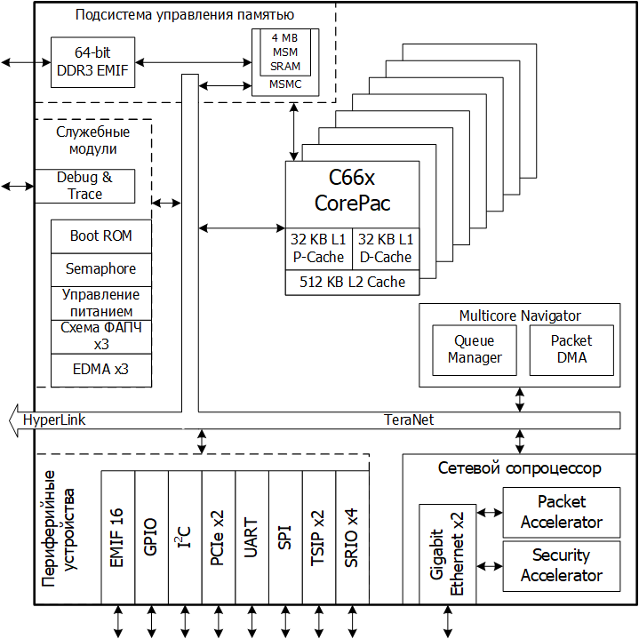
The architecture of the TMS320C6678 processor [2], the most high-performance processor in the TMS320C66xx family, is shown in Figure 1. The architecture can be broken down into the following main components:
')
Figure 1. The overall architecture of the processor TMS320C6678
The TMS320C6678 processor operates at a clock frequency of 1.25 GHz. The basis of the processor is a set of operating cores C66x CorePack, the number and composition of which depend on the specific processor model. The DSP TMS320C6678 includes 8 DSP-type cores. The kernel is the basic computational element and includes computational blocks, sets of registers, software, program memory and data. The memory that is part of the kernel is called local.
In addition to local memory, there is a memory shared by all cores — a shared multicore processor memory (Multicore Shared Memory - MSM). Shared memory is accessed through a memory subsystem (Memory Subsystem), which also includes an external EMIF memory interface for exchanging data between the processor and external memory chips.
The network coprocessor increases the efficiency of the processor as part of various telecommunication devices, realizing by hardware-standard data processing tasks for this area. The coprocessor is based on Packet Accelerator and Security Accelerator. The processor specification lists a set of protocols and standards supported by these accelerators.
Peripherals include:
Utility hardware modules include:
The internal transfer controller (Multicore Navigator) is a powerful and efficient hardware module that is responsible for arbitrating the transfer of data between various processor components. Multi-core systems on a chip TMS320C66xx are very complex devices and to organize the exchange of information between all components of such a device, you need a special hardware unit. Multicore Navigator allows cores, peripherals, and host devices not to take over the functions of controlling data exchange. When a processor component needs to send an array of data to another component, it simply tells the controller what to send and where. All functions on the transfer and synchronization of the sender and the recipient itself are taken over by the Multicore Navigator.
The basis of the multi-core processor TMS320C66xx in terms of high-speed data exchange between all the numerous components of the processor, as well as external modules, is the internal TeraNet bus.
The next article will look in detail at the architecture of the C66x operating core.
1. Multicore Programming Guide / SPRAB27B - August 2012;
2. TMS320C6678 Multicore Fixed and Floating Digital Signal Processor Data Manual / SPRS691C - February 2012.
Digital signal processors TMS320C66xx are built according to the KeyStone architecture and are high-performance multi-core signal processors that work with both fixed and floating point. The KeyStone architecture is a multi-core system-on-a-chip manufacturing principle developed by Texas Instruments that allows efficient collaboration of a large number of DSP and RISC types, accelerators and peripheral devices, ensuring sufficient bandwidth of internal and external data transfer channels, which are based on hardware components: Multicore Navigator (data exchange controller for internal interfaces), TeraNet (internal data transfer bus), Multicore Shared Memory Controller (access controller for shared memory) ) And HyperLink (interface with external devices on-chip rate).
The architecture of the TMS320C6678 processor [2], the most high-performance processor in the TMS320C66xx family, is shown in Figure 1. The architecture can be broken down into the following main components:
- a set of operating cores (CorePack);
- a subsystem for working with shared internal and external memory (Memory Subsystem);
- peripherals;
- network coprocessor (Network Coprocessor);
- Internal Shipping Controller (Multicore Navigator);
- service hardware modules and TeraNet internal bus.
')
Figure 1. The overall architecture of the processor TMS320C6678
The TMS320C6678 processor operates at a clock frequency of 1.25 GHz. The basis of the processor is a set of operating cores C66x CorePack, the number and composition of which depend on the specific processor model. The DSP TMS320C6678 includes 8 DSP-type cores. The kernel is the basic computational element and includes computational blocks, sets of registers, software, program memory and data. The memory that is part of the kernel is called local.
In addition to local memory, there is a memory shared by all cores — a shared multicore processor memory (Multicore Shared Memory - MSM). Shared memory is accessed through a memory subsystem (Memory Subsystem), which also includes an external EMIF memory interface for exchanging data between the processor and external memory chips.
The network coprocessor increases the efficiency of the processor as part of various telecommunication devices, realizing by hardware-standard data processing tasks for this area. The coprocessor is based on Packet Accelerator and Security Accelerator. The processor specification lists a set of protocols and standards supported by these accelerators.
Peripherals include:
- Serial RapidIO (SRIO) version 2.1 - provides data transfer rate up to 5 GBaud per line with the number of lines (channels) - up to 4;
- PCI Express (PCIe) version Gen2 - provides data transfer rate up to 5 GBaud per line with the number of lines (channels) - up to 2;
- HyperLink - an internal bus interface that allows you to switch processors built on the KeyStone architecture directly with each other and exchange at the on-chip speed; data transfer rate - up to 50 Gbaud;
- Gigabit Ethernet (GbE) provides transfer rates: 10/100/1000 Mbps and is supported by the hardware accelerator of network communications (network coprocessor);
- EMIF DDR3 - external memory interface type DDR3; has a 64-bit bus width providing addressable memory space of up to 8 GB;
- EMIF - general purpose external memory interface; has a bus width of 16 bits and can be used to connect 256MB NAND Flash or 16MB NOR Flash;
- TSIP (Telecom Serial Ports) - telecommunications serial port; provides transfer rates up to 8 Mbit / s per line with the number of lines up to 8;
- UART - universal asynchronous serial port;
- I2C - internal communication bus;
- GPIO - general-purpose input-output - 16 pins;
- SPI - Universal Serial Interface;
- Timers are used to generate periodic events.
Utility hardware modules include:
- debugging and tracing module (Debug and Trace) - allows debug tools access to internal resources of a running processor;
- boot ROM (boot ROM) - stores the boot program;
- hardware semaphore (semaphore) - is used for hardware support of the organization of joint access of parallel processes to common processor resources;
- power management module - implements dynamic control of the power modes of the processor components in order to minimize power consumption at the moments when the processor is not working at full power;
- PLL - forms the internal clock frequency of the processor from an external reference clock signal;
- Direct Memory Access Controller (EDMA) - manages the data transfer process by unloading the DSP cores and being an alternative to the Multicore Navigator.
The internal transfer controller (Multicore Navigator) is a powerful and efficient hardware module that is responsible for arbitrating the transfer of data between various processor components. Multi-core systems on a chip TMS320C66xx are very complex devices and to organize the exchange of information between all components of such a device, you need a special hardware unit. Multicore Navigator allows cores, peripherals, and host devices not to take over the functions of controlling data exchange. When a processor component needs to send an array of data to another component, it simply tells the controller what to send and where. All functions on the transfer and synchronization of the sender and the recipient itself are taken over by the Multicore Navigator.
The basis of the multi-core processor TMS320C66xx in terms of high-speed data exchange between all the numerous components of the processor, as well as external modules, is the internal TeraNet bus.
The next article will look in detail at the architecture of the C66x operating core.
1. Multicore Programming Guide / SPRAB27B - August 2012;
2. TMS320C6678 Multicore Fixed and Floating Digital Signal Processor Data Manual / SPRS691C - February 2012.
Source: https://habr.com/ru/post/331684/
All Articles