IBM introduced the world's first 5-nanometer chip
IBM, working together with Samsung and GlobalFoundries, introduced the world's first silicon chip, made on the 5-nm process technology. This chip was also the first to use horizontally-located rotary-gate transistors (GAAFET) and photolithography technology was used in the deep ultraviolet (EUV).
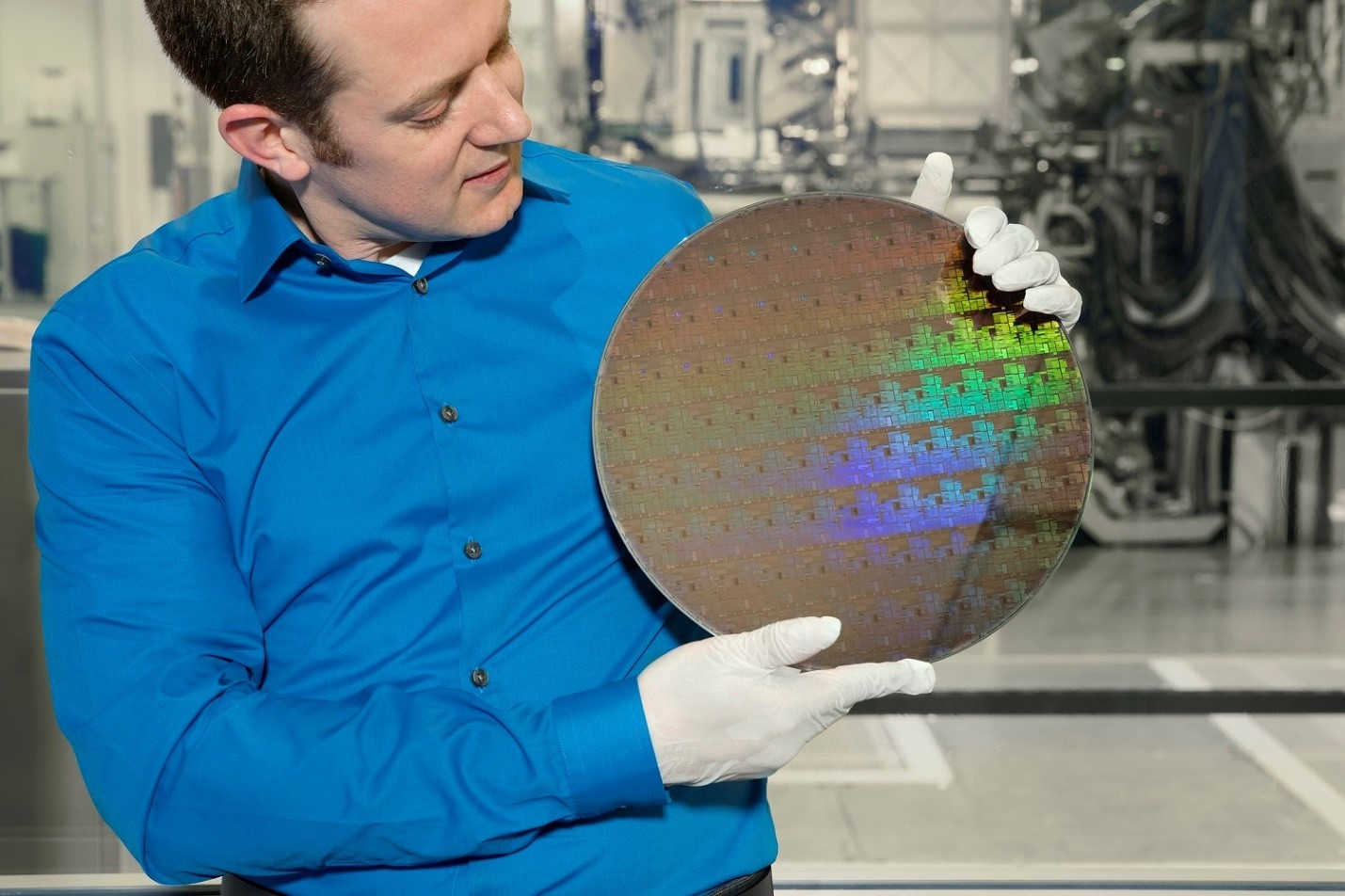 / photo IBM Research CC
GAAFET is a development of finFET technology based on transistors with a vertically located gate resembling a “fin”, which today is used to make most chips with technical processes of 22 nm or less. Scientists from IBM, Samsung and GloFo deployed the finFET architecture by 90 degrees, which made it possible to form a horizontal fin that acts as a nanowire stretched from the source to the drain.
')
IBM's GAAFET has three nano-sheets placed on top of each other and passing between the drain and the source. The shutter in this design is quite large, which guarantees the reliability of the architecture and its performance.
 / photo IBM Research CC
One of the main advantages of the 5-nm GAAFET from IBM is a significant reduction in the complexity of the formation of the pattern. Huiming Bu, the head of IBM Research, which develops silicon devices, notes that the new 5-nm chip was the first to use photolithography in the deep ultraviolet to apply semiconductor structures. EUV technology uses a shorter wavelength (13.5 nm) than in modern installations for immersion lithography (193 nm), which reduces the number of drawing steps.
IBM noted that they managed to fit 30 billion transistors into a chip of 50 square millimeters. For comparison, a similar-in-area chip manufactured using the 7-nm process only holds 20 billion transistors.
Also, company representatives said that compared to commercial 10-nm chips, the new 5-nm chips offer a 40% increase in performance with the same power consumption, or 75% reduction in power consumption while maintaining the speed of 10-nm devices.
The start date of the industrial production of new processors at IBM was not named.
IBM is an American company, one of the world's largest manufacturers and suppliers of hardware and software, as well as IT services and consulting services.
Samsung is a South Korean group of companies, founded in 1938. On the world market it is known as a manufacturer of high-tech components, telecommunications equipment, household appliances, audio and video devices. The main office of the company is located in Seoul.
GlobalFoundries is an American company that is the third largest contract manufacturer of semiconductor integrated circuits. It was founded in 2009 on the basis of the production unit of the company AMD.
PS Other materials from our blog:
/ photo IBM Research CCGAAFET is a development of finFET technology based on transistors with a vertically located gate resembling a “fin”, which today is used to make most chips with technical processes of 22 nm or less. Scientists from IBM, Samsung and GloFo deployed the finFET architecture by 90 degrees, which made it possible to form a horizontal fin that acts as a nanowire stretched from the source to the drain.
')
IBM's GAAFET has three nano-sheets placed on top of each other and passing between the drain and the source. The shutter in this design is quite large, which guarantees the reliability of the architecture and its performance.
/ photo IBM Research CCOne of the main advantages of the 5-nm GAAFET from IBM is a significant reduction in the complexity of the formation of the pattern. Huiming Bu, the head of IBM Research, which develops silicon devices, notes that the new 5-nm chip was the first to use photolithography in the deep ultraviolet to apply semiconductor structures. EUV technology uses a shorter wavelength (13.5 nm) than in modern installations for immersion lithography (193 nm), which reduces the number of drawing steps.
IBM noted that they managed to fit 30 billion transistors into a chip of 50 square millimeters. For comparison, a similar-in-area chip manufactured using the 7-nm process only holds 20 billion transistors.
Also, company representatives said that compared to commercial 10-nm chips, the new 5-nm chips offer a 40% increase in performance with the same power consumption, or 75% reduction in power consumption while maintaining the speed of 10-nm devices.
The start date of the industrial production of new processors at IBM was not named.
About IBM
IBM is an American company, one of the world's largest manufacturers and suppliers of hardware and software, as well as IT services and consulting services.
About Samsung
Samsung is a South Korean group of companies, founded in 1938. On the world market it is known as a manufacturer of high-tech components, telecommunications equipment, household appliances, audio and video devices. The main office of the company is located in Seoul.
About GlobalFoundries
GlobalFoundries is an American company that is the third largest contract manufacturer of semiconductor integrated circuits. It was founded in 2009 on the basis of the production unit of the company AMD.
PS Other materials from our blog:
- Cloud technology in construction
- KUBIT: the organization of integrated IT solutions using IaaS-cloud "IT-GRAD"
- Animal Behavioral Analysis: How the IaaS Cloud Helps Predict Earthquakes
- IaaS in the world of music: how the cloud becomes the standard for placing audio content
- Cloud technologies for solving problems in the construction business
- Game industry: how IaaS gave a new life to the popular game Angry Birds
Source: https://habr.com/ru/post/330304/
All Articles