Porting MIPSfpga to other cards and integrating peripherals into the system. Part 2
MIPSfpga microprocessor MIPS32 microAptiv described in Verilog language for educational purposes of the company Imagination, which has a cache memory and a memory management unit. The processor code is available to the user ( download instructions ) and can be used to simulate and implement a processor on an FPGA board.
This article is a continuation of the article on how to port MIPSfpga-plus to other boards , and it will describe how to integrate peripherals into the MIPSfpga-plus system using the example of 16 Digillent Pmod KYPD keyboard:
')
Connecting the keyboard to the processor will allow the user to communicate with him. In general, 16-button keypads come in different representations, but the implementation and operation principle is the same for them. Therefore, according to this example, similar keyboards can be integrated.
The integration of the built-in ADC board, as well as the display connections from the Nokia 5100 is described in the following part of my tutorial:
Porting MIPSfpga to other cards and integrating peripherals into the system. Part 3
Also, how to start working with MIPSfpga is written in the article .
MIPS architecture is one of the first computer architectures with reduced instruction set (RISC). It emerged as a result of research at Stanford University in 1981 and revolutionized the efficiency of computer architectures. The commercial use of MIPS architecture began in 1984 by MIPSfpga 2: Getting Started Imagination Technologies v1.3, March 1, 2016 MIPS Computer Systems, which in 2013 was acquired by Imagination Technologies.
MIPS processors were used in Silicon Graphics high-performance workstations that were manufactured in the 1980s and 1990s. The first commercially successful product was the MIPS R3000 processor, which had a five-stage pipeline. It was followed by the R4000, which added 64-bit commands, a superscalar R8000, a processor with an extraordinary execution of R10000 commands, and many other high-performance cores.
Over time, the MIPS architecture has evolved for applications in low-cost, low-power products, such as consumer electronics, networking equipment, and microcontrollers. The M4K family is based on the classic 32-bit architecture with a five-stage pipeline. In the M14K family, a set of 16-bit microMIPS instructions has been added, which allows reducing the size of programs for embedded applications, in which cost is very important. In the microAptiv family, the M14K instruction set is extended with additional digital signal processing instructions. The M14K core exists in two versions: microcontroller (UC) and microprocessor (UP). The microprocessor version contains cache memory and supports virtual memory, which provides the ability to run an operating system such as Linux or Android. Perhaps you are familiar with Microchip's popular PIC32 microcontroller line, which is based on the M4K architecture.
The processor uses a memory interface to communicate with peripheral devices. That is, this means that data is written and read from the connected peripherals in the same way as from a RAM block. The integration of peripherals into the processor is carried out by connecting to the AHB-Lite bus ( detailed documentation ). Try to understand the connection process in more detail.
First you need to have an idea of how the signals will pass through the AHB-Lite bus:
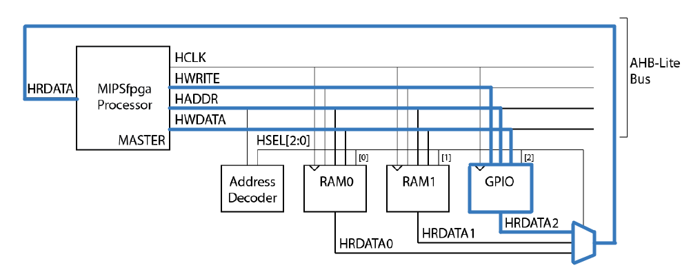
It is seen that the process of reading data from the periphery is carried out by the HRDATA signal, data is transmitted via HWRITE with an active high level on the write resolution signal, the choice of GPIO is performed by selecting the address on HADDR.
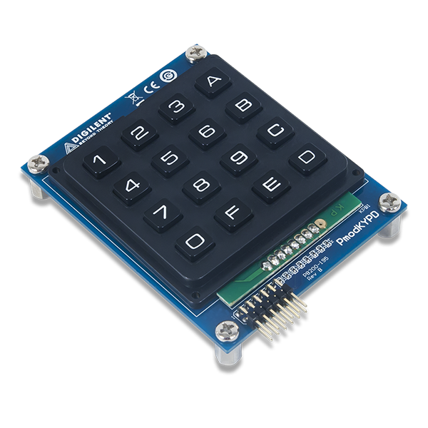
The first sensor that was connected is the 16-button pmod KYPD ( datasheet ).
In my case, the Pmod interface was used to connect the keyboard, but you can use any other pins of your board, but then you will need to register them in the file with * .xdc restrictions. To which pins to connect the keyboard is described below in the table.
Pinout and keyboard signals are described in the table:
Keyboard wiring is very simple:
The next step to integrate the keyboard to the AHB-lite bus is to write a module on Verilog.
The keyboard uses 4 rows and columns to create an array of 16 clock buttons.
The diagram shows that the rows are pulled up to the power supply with resistances at R = 10k, which means that by actuating the lines of the columns to a low logic level, a clock signal with a certain frequency is supplied. At the moment when the active signal at the input coincides with the column (col) on which the button is pressed, a low level will appear at the output of the row. To implement such a process, you need to write a decoder (an example of the implementation of the module is also described in this article ).

The module itself has the form:
The scheme of the module in Vivado will be:

In short, you need to add the decoder module to the Vivado project as follows: Add Sources → Add → create → → → Create File → (write the file name) → Ok → Ok → Ok → Yes. An empty Verilog file was created, after creating the file, you need to find it in the hierarchy of the MIPSfpga-plus system, write the decoder code and save it. A more detailed description of how to add a module to a project and just how to work with Vivado is described in my previous article:
Porting MIPSfpga to other cards and integrating peripherals into the system. Part 1
Now let's get down to connecting the inputs and outputs to the AHB-Lite bus and the physical outputs of our board.
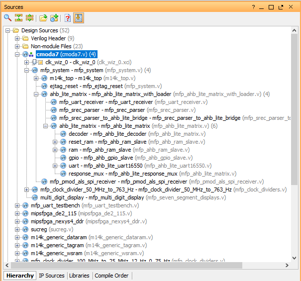
The mipsfpga_ahb hierarchy is:
For starters, in the Verilog Header directory, mfp_ahb_lite_matrix_config.vh, we will specify using the `define directive name of the peripheral we will connect. To do this, we will find a line with the identifier for adding an illumination sensor to the system (for more information about the sensor, see the previous article):
The line needs to be commented out, this will turn off all the lines related to the connection code of the light sensor to the AHB-Lite bus:
Let's write and uncomment the line for our periphery:
Open “mfp_system” and find the connection strings for the instance of the light sensor:
And next we add an instance of your decoder module:
The signals of the decoder module need to be connected to the bus instance mfp_ahb_lite_matrix_with_loader (where you can watch the required lines using the example of the integration of the illumination sensor using the module MFP_DEMO_LIGHT_SENSOR):
To connect the instances of the decoder module and bus, add a signal of the wire type:
After connecting our decoder module to the bus, go to “mfp_ahb_lite_matrix_with_loader” which is located in the hierarchy below the “mfp_system” module and add an input / output port:
Also add these signals to the instance “mfp_ahb_lite_matrix”:
We will do the same in “mfp_ahb_lite_matrix” which is located in the hierarchy below the “mfp_ahb_lite_matrix_with_loader” module and add an input / output port:
Also add these signals to the instance “mfp_ahb_gpio_slave”:
Let's go to the “mfp_ahb_gpio_slave” module, this is exactly the block (GPIO) in which we were so torn, we will add an input / output port:
Now we need to change the “mfp_ahb_gpio_slave” module so that it detects the I / O address with memory mapping (which we still define) and writes the data (HWDATA) into the register corresponding to the detected address:
To specify the address at which we will contact, open the header file "mfp_ahb_lite_matrix_config.vh" and add:
The GPIO module uses the lower bits of the address to determine which peripheral device should read or write information.
Let's go back through the hierarchy to the mfp_system module and add I / O ports:
It is worth noting that these are not exactly the ports that we connected to the bus. Go to the top module shell (I have "cmoda7") and add to the instance "mfp_system" line:
Thus, we added the module of our decoder to JA [7: 0] pins and connected the decoder to the processor via the AHB-Lite bus.
In our case, the JA I / O ports in the module shell and in the restriction file (I have “cmoda7.xdc”) will not need to be added because they have already been used for the light sensor. But in other cases, such actions will be required, because for understanding I will simply show these lines:
And if we recall in “mfp_ahb_lite_matrix_config.vh” we commented out the line:
thus, during the synthesis of the system, all the code written between
will be ignored, and there will be no port conflicts.
We can see the scheme of the created MIPSfpga-plus system with a built-in decoder for our keyboard, for this, open the tab RTL Analysys → Open Elaborated Design → Schematic. The entire system diagram is displayed here to check the correctness of the connected module of the decoder, it is advisable to go through the RTL Netlist and check all contacts.
Now you can generate a bitstream file (.bit) and load it into FPGA.
We write a simple program for the interaction of the keyboard and processor.
To download the code to the system, go to the folder downloaded mipsfpga plus → github → mipsfpga-plus → programs → 01_pmod_kypd open “mfp_memory_mapped_registers.h”
next, open main.c and write a couple of lines to demonstrate:
After in the folder we find the script that compiles the code:
Generate the motorola_s_record file:
Check to which COM port the USB UART converter is connected:
Modify the 12_upload_to_the_board_using_uart file:
where a is the number of the COM port to which the USB UART converter is connected. And load the program:
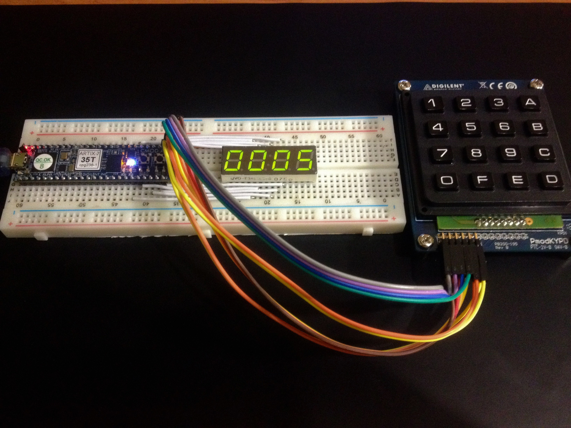
Result:
In the next part, I’ll tell you how to add to the MIPSfpga built-in cmoda7 OCA, and LCD display from Nokia 5100.
Porting MIPSfpga to other cards and integrating peripherals into the system. Part 3
This article is a continuation of the article on how to port MIPSfpga-plus to other boards , and it will describe how to integrate peripherals into the MIPSfpga-plus system using the example of 16 Digillent Pmod KYPD keyboard:
')
Connecting the keyboard to the processor will allow the user to communicate with him. In general, 16-button keypads come in different representations, but the implementation and operation principle is the same for them. Therefore, according to this example, similar keyboards can be integrated.
The integration of the built-in ADC board, as well as the display connections from the Nokia 5100 is described in the following part of my tutorial:
Porting MIPSfpga to other cards and integrating peripherals into the system. Part 3
Also, how to start working with MIPSfpga is written in the article .
MIPS architecture is one of the first computer architectures with reduced instruction set (RISC). It emerged as a result of research at Stanford University in 1981 and revolutionized the efficiency of computer architectures. The commercial use of MIPS architecture began in 1984 by MIPSfpga 2: Getting Started Imagination Technologies v1.3, March 1, 2016 MIPS Computer Systems, which in 2013 was acquired by Imagination Technologies.
MIPS processors were used in Silicon Graphics high-performance workstations that were manufactured in the 1980s and 1990s. The first commercially successful product was the MIPS R3000 processor, which had a five-stage pipeline. It was followed by the R4000, which added 64-bit commands, a superscalar R8000, a processor with an extraordinary execution of R10000 commands, and many other high-performance cores.
Over time, the MIPS architecture has evolved for applications in low-cost, low-power products, such as consumer electronics, networking equipment, and microcontrollers. The M4K family is based on the classic 32-bit architecture with a five-stage pipeline. In the M14K family, a set of 16-bit microMIPS instructions has been added, which allows reducing the size of programs for embedded applications, in which cost is very important. In the microAptiv family, the M14K instruction set is extended with additional digital signal processing instructions. The M14K core exists in two versions: microcontroller (UC) and microprocessor (UP). The microprocessor version contains cache memory and supports virtual memory, which provides the ability to run an operating system such as Linux or Android. Perhaps you are familiar with Microchip's popular PIC32 microcontroller line, which is based on the M4K architecture.
The processor uses a memory interface to communicate with peripheral devices. That is, this means that data is written and read from the connected peripherals in the same way as from a RAM block. The integration of peripherals into the processor is carried out by connecting to the AHB-Lite bus ( detailed documentation ). Try to understand the connection process in more detail.
First you need to have an idea of how the signals will pass through the AHB-Lite bus:
It is seen that the process of reading data from the periphery is carried out by the HRDATA signal, data is transmitted via HWRITE with an active high level on the write resolution signal, the choice of GPIO is performed by selecting the address on HADDR.
1. Keyboard connection Digilent Pmod KYPD
The first sensor that was connected is the 16-button pmod KYPD ( datasheet ).
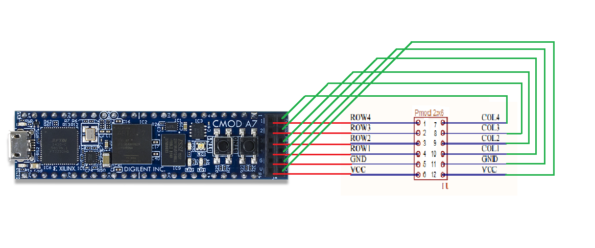
In my case, the Pmod interface was used to connect the keyboard, but you can use any other pins of your board, but then you will need to register them in the file with * .xdc restrictions. To which pins to connect the keyboard is described below in the table.
Pinout and keyboard signals are described in the table:
| Pin | Signal | Purpose | Pin | Signal | Purpose |
|---|---|---|---|---|---|
| one | Col4 | 4 column | 7 | ROW4 | 4 row |
| 2 | Col3 | 3 column | eight | ROW3 | 3 row |
| 3 | Col2 | 2 column | 9 | ROW2 | 2 row |
| four | Col1 | 1 column | ten | ROW1 | 1 row |
| five | GND | ground contact | eleven | GND | ground contact |
| 6 | GND | power contact | 12 | VCC | power contact |
Keyboard wiring is very simple:
The next step to integrate the keyboard to the AHB-lite bus is to write a module on Verilog.
The keyboard uses 4 rows and columns to create an array of 16 clock buttons.
The diagram shows that the rows are pulled up to the power supply with resistances at R = 10k, which means that by actuating the lines of the columns to a low logic level, a clock signal with a certain frequency is supplied. At the moment when the active signal at the input coincides with the column (col) on which the button is pressed, a low level will appear at the output of the row. To implement such a process, you need to write a decoder (an example of the implementation of the module is also described in this article ).
The module itself has the form:
module kypd_decoder( input i_clk, input i_rst_n, input [3:0] i_row, output reg [3:0] o_col, output reg [3:0] o_number ); reg [19:0] counter; reg [3:0] col; reg [3:0] row; // row col parameter ZERO = 8'b11100111, ONE = 8'b01110111, TWO = 8'b01111011, THREE = 8'b01111101, FOUR = 8'b10110111, FIVE = 8'b10111011, SIX = 8'b10111101, SEVEN = 8'b11010111, EIGHT = 8'b11011011, NINE = 8'b11011101, A = 8'b01111110, B = 8'b10111110, C = 8'b11011110, D = 8'b11101110, E = 8'b11101101, F = 8'b11101011; always @(posedge i_clk or negedge i_rst_n) if (i_rst_n == 0) counter <= 20'b0; else counter <= counter + 1'b1; always @(posedge i_clk or negedge i_rst_n) if (i_rst_n == 1'b0) begin o_col <= 4'b1110; col <= 4'b1110; row <= 4'b1111; end else if (!counter) begin o_col <= {o_col [0], o_col [3:1]}; col <= o_col; row <= i_row; end always @(posedge i_clk or negedge i_rst_n) if (i_rst_n == 0) o_number <= 4'b0; else case ({row, col}) ZERO: o_number <= 4'h0; ONE: o_number <= 4'h1; TWO: o_number <= 4'h2; THREE: o_number <= 4'h3; FOUR: o_number <= 4'h4; FIVE: o_number <= 4'h5; SIX: o_number <= 4'h6; SEVEN: o_number <= 4'h7; EIGHT: o_number <= 4'h8; NINE: o_number <= 4'h9; A: o_number <= 4'hA; B: o_number <= 4'hB; C: o_number <= 4'hC; D: o_number <= 4'hD; E: o_number <= 4'hE; F: o_number <= 4'hF; endcase endmodule The scheme of the module in Vivado will be:
In short, you need to add the decoder module to the Vivado project as follows: Add Sources → Add → create → → → Create File → (write the file name) → Ok → Ok → Ok → Yes. An empty Verilog file was created, after creating the file, you need to find it in the hierarchy of the MIPSfpga-plus system, write the decoder code and save it. A more detailed description of how to add a module to a project and just how to work with Vivado is described in my previous article:
Porting MIPSfpga to other cards and integrating peripherals into the system. Part 1
Now let's get down to connecting the inputs and outputs to the AHB-Lite bus and the physical outputs of our board.
The mipsfpga_ahb hierarchy is:
For starters, in the Verilog Header directory, mfp_ahb_lite_matrix_config.vh, we will specify using the `define directive name of the peripheral we will connect. To do this, we will find a line with the identifier for adding an illumination sensor to the system (for more information about the sensor, see the previous article):
The line needs to be commented out, this will turn off all the lines related to the connection code of the light sensor to the AHB-Lite bus:
//`define MFP_DEMO_LIGHT_SENSOR Let's write and uncomment the line for our periphery:
`define MFP_PMOD_KYPD Open “mfp_system” and find the connection strings for the instance of the light sensor:
`ifdef MFP_DEMO_LIGHT_SENSOR And next we add an instance of your decoder module:
`ifdef MFP_PMOD_KYPD kypd_decoder kypd_decoder ( .i_clk ( SI_ClkIn ), .i_rst_n ( KEY_0 ), .o_col ( KYPD_DATA [3:0] ), .i_row ( KYPD_DATA [7:4] ), .o_number ( KYPD_OUT ) ); `endif The signals of the decoder module need to be connected to the bus instance mfp_ahb_lite_matrix_with_loader (where you can watch the required lines using the example of the integration of the illumination sensor using the module MFP_DEMO_LIGHT_SENSOR):
`ifdef MFP_PMOD_KYPD .KYPD_OUT ( KYPD_OUT ), `endif To connect the instances of the decoder module and bus, add a signal of the wire type:
`ifdef MFP_PMOD_KYPD wire [3:0] KYPD_OUT; `endif After connecting our decoder module to the bus, go to “mfp_ahb_lite_matrix_with_loader” which is located in the hierarchy below the “mfp_system” module and add an input / output port:
`ifdef MFP_PMOD_KYPD input [3:0] KYPD_OUT, `endif Also add these signals to the instance “mfp_ahb_lite_matrix”:
`ifdef MFP_PMOD_KYPD .KYPD_OUT ( KYPD_OUT ), `endif We will do the same in “mfp_ahb_lite_matrix” which is located in the hierarchy below the “mfp_ahb_lite_matrix_with_loader” module and add an input / output port:
`ifdef MFP_PMOD_KYPD input [3:0] KYPD_OUT, `endif Also add these signals to the instance “mfp_ahb_gpio_slave”:
`ifdef MFP_PMOD_KYPD .KYPD_OUT ( KYPD_OUT ), `endif Let's go to the “mfp_ahb_gpio_slave” module, this is exactly the block (GPIO) in which we were so torn, we will add an input / output port:
`ifdef MFP_PMOD_KYPD input [3:0] KYPD_OUT, `endif Now we need to change the “mfp_ahb_gpio_slave” module so that it detects the I / O address with memory mapping (which we still define) and writes the data (HWDATA) into the register corresponding to the detected address:
`ifdef MFP_PMOD_KYPD `MFP_PMOD_KYPD_IONUM : HRDATA <= { 28'b0, KYPD_OUT }; `endif To specify the address at which we will contact, open the header file "mfp_ahb_lite_matrix_config.vh" and add:
`ifdef MFP_PMOD_KYPD `define MFP_PMOD_KYPD_ADDR 32'h1f800018 `endif The GPIO module uses the lower bits of the address to determine which peripheral device should read or write information.
`ifdef MFP_PMOD_KYPD `define MFP_PMOD_KYPD_IONUM 4'h6 `endif Let's go back through the hierarchy to the mfp_system module and add I / O ports:
`ifdef MFP_PMOD_KYPD inout [7:0] KYPD_DATA, input KEY_0, `endif It is worth noting that these are not exactly the ports that we connected to the bus. Go to the top module shell (I have "cmoda7") and add to the instance "mfp_system" line:
`ifdef MFP_PMOD_KYPD .KYPD_DATA ( JA ), .KEY_0 ( ~ i_btn1 ), `endif Thus, we added the module of our decoder to JA [7: 0] pins and connected the decoder to the processor via the AHB-Lite bus.
In our case, the JA I / O ports in the module shell and in the restriction file (I have “cmoda7.xdc”) will not need to be added because they have already been used for the light sensor. But in other cases, such actions will be required, because for understanding I will simply show these lines:
module cmoda7 ( ... ... ... inout [ 7:0] JA ); cmoda7.xdc
## Pmod Header JA set_property -dict {PACKAGE_PIN G17 IOSTANDARD LVCMOS33} [get_ports {JA[0]}] set_property -dict {PACKAGE_PIN G19 IOSTANDARD LVCMOS33} [get_ports {JA[1]}] set_property -dict {PACKAGE_PIN N18 IOSTANDARD LVCMOS33} [get_ports {JA[2]}] set_property -dict {PACKAGE_PIN L18 IOSTANDARD LVCMOS33} [get_ports {JA[3]}] set_property -dict {PACKAGE_PIN H17 IOSTANDARD LVCMOS33} [get_ports {JA[4]}] set_property -dict {PACKAGE_PIN H19 IOSTANDARD LVCMOS33} [get_ports {JA[5]}] set_property -dict {PACKAGE_PIN J19 IOSTANDARD LVCMOS33} [get_ports {JA[6]}] set_property -dict {PACKAGE_PIN K18 IOSTANDARD LVCMOS33} [get_ports {JA[7]}] And if we recall in “mfp_ahb_lite_matrix_config.vh” we commented out the line:
//`define MFP_DEMO_LIGHT_SENSOR thus, during the synthesis of the system, all the code written between
`ifdef MFP_DEMO_LIGHT_SENSOR ... `endif will be ignored, and there will be no port conflicts.
We can see the scheme of the created MIPSfpga-plus system with a built-in decoder for our keyboard, for this, open the tab RTL Analysys → Open Elaborated Design → Schematic. The entire system diagram is displayed here to check the correctness of the connected module of the decoder, it is advisable to go through the RTL Netlist and check all contacts.
Now you can generate a bitstream file (.bit) and load it into FPGA.
We write a simple program for the interaction of the keyboard and processor.
To download the code to the system, go to the folder downloaded mipsfpga plus → github → mipsfpga-plus → programs → 01_pmod_kypd open “mfp_memory_mapped_registers.h”
#define MFP_PMOD_KYPD_ADDR 0xBF800018 #define MFP_PMOD_KYPD (* (volatile unsigned *) MFP_PMOD_KYPD_ADDR ) next, open main.c and write a couple of lines to demonstrate:
#include "mfp_memory_mapped_registers.h" int main () { int n = 0; for (;;) { MFP_7_SEGMENT_HEX = MFP_PMOD_KYPD; } return 0; } After in the folder we find the script that compiles the code:
02_compile_and_link Generate the motorola_s_record file:
08_generate_motorola_s_record_file Check to which COM port the USB UART converter is connected:
11_check_which_com_port_is_used Modify the 12_upload_to_the_board_using_uart file:
set a=7 mode com%a% baud=115200 parity=n data=8 stop=1 to=off xon=off odsr=off octs=off dtr=off rts=off idsr=off type program.rec >\.\COM%a% where a is the number of the COM port to which the USB UART converter is connected. And load the program:
12_upload_to_the_board_using_uart Result:
In the next part, I’ll tell you how to add to the MIPSfpga built-in cmoda7 OCA, and LCD display from Nokia 5100.
Porting MIPSfpga to other cards and integrating peripherals into the system. Part 3
Source: https://habr.com/ru/post/329852/
All Articles