Porting MIPSfpga to other cards and integrating peripherals into the system. Part 1
MIPSfpga is an educationally designed microprocessor MIPS32 microAptiv of Imagination, which has a cache memory and a memory management unit. The Verilog processor code is available to the user and can be used to simulate and implement a processor on an FPGA board.
This article will describe, using the example of Digilent cmodA7, how to port the MIPSfpga-plus processor to other cards.
')
To date, MIPSFPGA has been ported to popular boards from companies such as ALTERA and Xilinx, among them Basys 3, Nexys4 ddr, and others (the full list is on github ). Such boards are most popular among developers on FPGA. The price of such boards is not quite small, and the programs are loaded into the MIPSfpga core using the EJTAG interface and the Bus Blaster adapter at the cost of about $ 50. The Bus Blaster adapter receives commands via a high-speed USB 2.0 cable and converts them to the serial protocol EJTAG, which allows you to load programs into the MIPSfpga core and control the debugging of the programs that run on it. The problem with relatively expensive Bus Blaster was solved by introducing a number of improvements to the MIPSfpga system. An improved version of the MIPSfpga system, called MIPSfpga-plus, includes such new features:
- Ability to download software using a USB-to-UART connector priced at $ 5 FTDI instead of $ 50 Bus Blaster, which sometimes is not so easy to get.
- The ability to change the clock frequency on the fly from 50 or 25 MHz to 1 Hz (one cycle per second) to monitor the processor in real time, including misses in the cache memory and redirection of the conveyor.
- An example of the integration of the light sensor with the SPI protocol.
- A small software initialization sequence that fits into 1 KB instead of 32 KB of memory, which allows MIPSfpga to be transferred to a wider choice of FPGA cards without using external memory. UART implementation is described in the article: MIPSfpga and UART .
Before adding various peripherals to MIPSfpga +, you need to load and run the system on the FPGA. Some steps of this manual can be skipped if you have a fee from the list below:
MIPSfpga-plus has already been ported to these boards and you can download it at the link:
github.com/MIPSfpga/mipsfpga-plus/tree/master/boards
In another case, if you have a different motherboard from the FPGA listed in the list, it will not be too difficult to port the processor to it. To do this, the following instruction is written, which is shown on the example of my cmodA7 board.
1. First you need to get a package with the MIPSFPGA system. Detailed instructions on how to do this:
→ mipsfpga-download-instruction
You will also need to download the current version of the MIPSfpga-plus extension:
→ Mipsfpga-plus
2. For Xilinx boards, Vivado software is used, the current version can be downloaded at the link:
→ Download Vivado
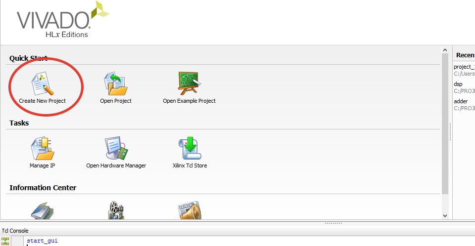
3. Now let's create a new project in Vivado:
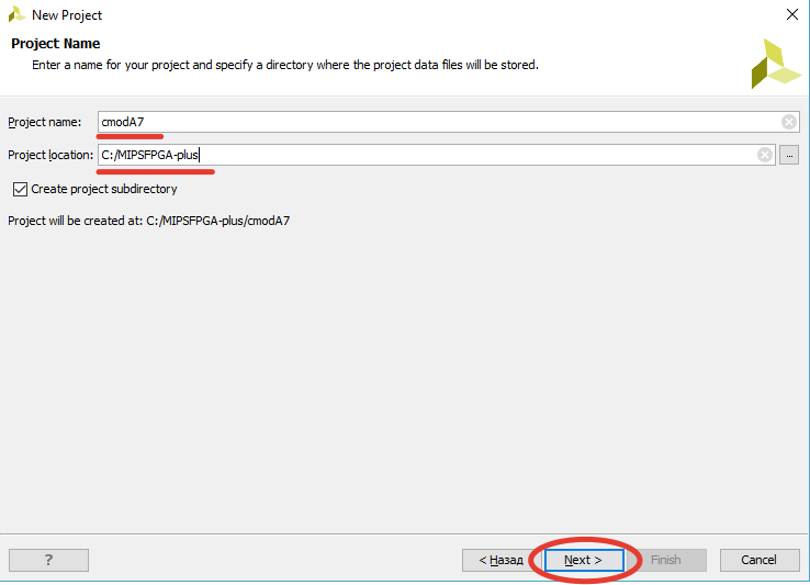
Choose where the created project will be stored:
Click next:

Select the RTL project and click on:

Now add the files of the original MIPSfpga system:


As well as MIPSfpga-plus which are in the archive downloaded from mipsfpga-plus :

Add to the project the uart module that was previously discussed:

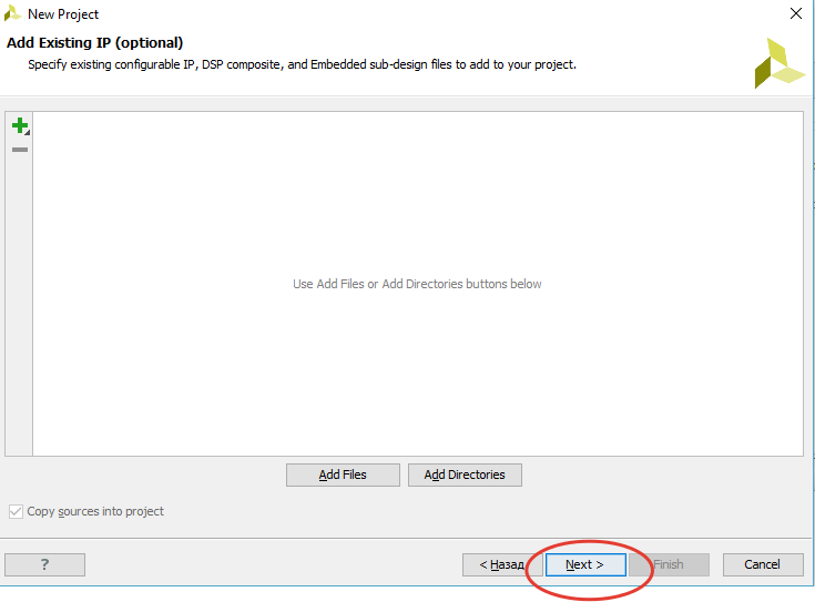
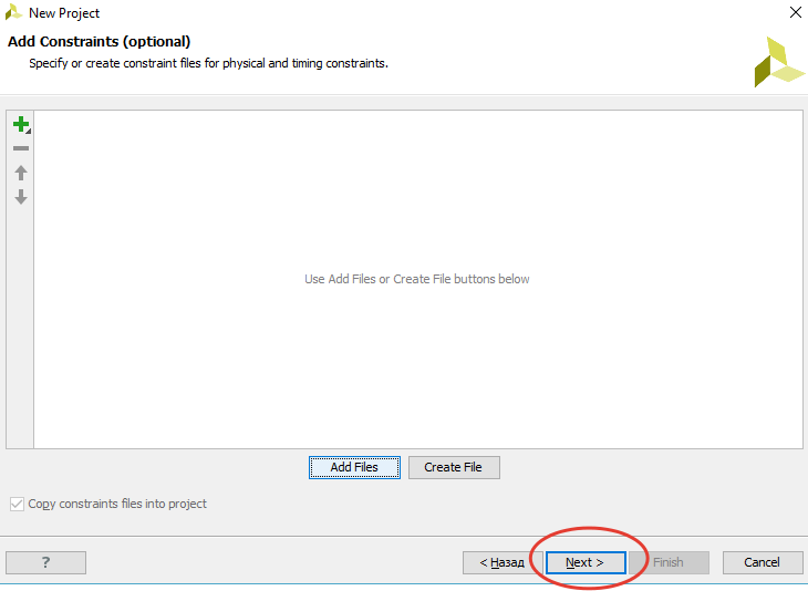
Skipping the creation of IP and construction files will create them later:
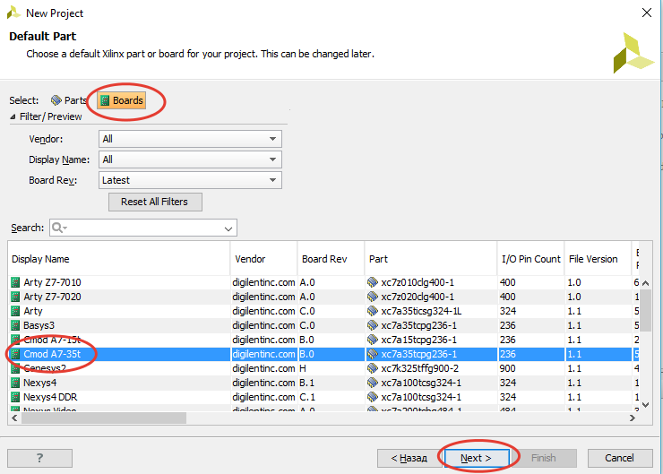
Next you need to either choose a chip or add your board.
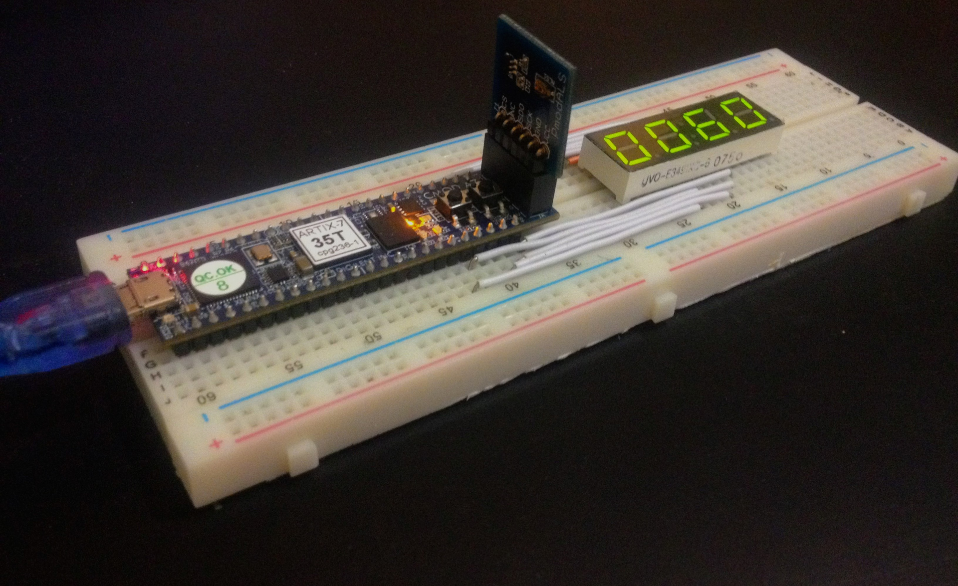
The Digilent cmod A7 board was chosen due to its low price and the presence of the ADC we use later. To select the FPGA scheme, you need to read the documentation on your board, on cmodA7 the xc7a35tcpg236-1 chip is placed:

Another way is to add your board file to the Vivado library, this method is better because, firstly, it is more convenient to remember the name of the board than the chip, and secondly, if you want to use the block designer in Vivado in the future, then you will have additional tools for convenient work with board interfaces, IP cores, etc. You can download them on GitHub , you need to save these files in ~ \ Vivado \ 2015.1 \ data \ boards \ (relevant for Vivado 2015.1 and newer).

So we created a project with MIPSfpga-plus.
In short, the Artix-7 chip is on board the cmodA7 board, it has 20800 LUT, 41600 FF, 225 KB block memory, 48 pins, 2 of which are ADC outputs, also a usb-uart converter, Quad-SPI Flash, and JTAG, 2 clock buttons, as well as 5 LEDs 3 of which are RGB ( datashit ).
To transfer the MIPSfpga system to the cmodA7 board, you should:
Step 1. Write a shell module that establishes the correspondence between the I / Os of the MIPSfpga and the I / Os of the cmodA7 board.
Step 2. Reduce the memory capacity of the MIPSfpga system to match the cmodA7 board.
Step 3. Add a constraint file that establishes the correspondence between the board I / Os and the FPGA chassis.


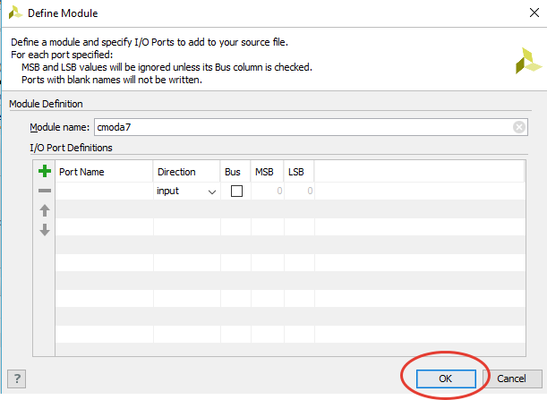
Install cmoda7.v as the top module in the system hierarchy.
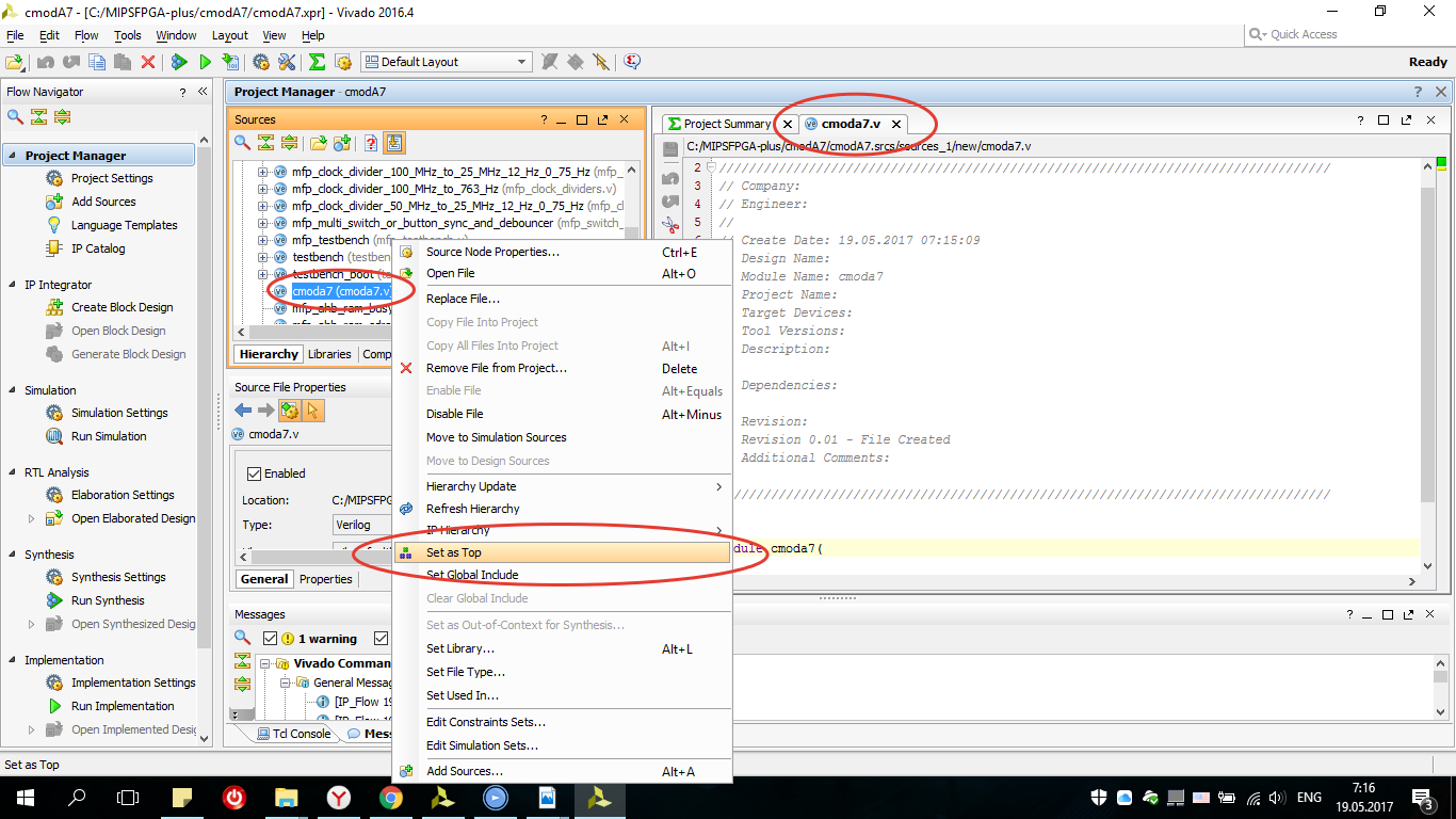
Since there are no switches on the cmoda7 board that could be used to lower the processor frequency (this modification appeared in MIPSfpga-plus), this module was simply not included in the shell module. You can also exclude the EJTAG output to which the BUS Blaster is connected.
First you need to add the header file for the AHB_lite bus configuration.
The Advanced High-Performance Bus (AHB) is an open interface that is used in many microprocessor-based systems, especially embedded ones. AHB bus facilitates the organization of the connection of multiple devices. AHB-Lite is a simplified version of AHB with one master device.

This configuration has one master device, a MIPSfpga processor, and three slaves: RAM0, RAM1, and GPIO, which are (respectively) two blocks of RAM and a module for accessing board I / O devices. We will just work with the GPIO block and write modules for interaction with peripherals.
Let's write the main input-output ports:
i_clk is the signal of the clock generator of the board frequency (for cmodA7 12 MHz).
i_btn0 - the button is used to reset the processor.
i_btn1 - n / c.
RsRx - receive signal by uart.
seg, dp, an, - contacts for connecting a seven-segment 4-digit indicator.
led_r, led_g, led_b, - the conclusions of the RGB Led placed on the board.
JA - Pmod interface.
The main signals are the clock signal and reset (i_btn0) others for connecting peripherals.

The main purpose of the cmoda7.v module is to create an instance of the MIPSfpga-plus system (mipsfpga_sys) and its connection to the I / O of the board.
MFP_DEMO_LIGHT_SENSOR will be used when testing a ported system. As you can see, at the output of the mfp_system system there will be a 32-bit IO_7_SegmentHEX bus which we output to the 4-digit 7 segment indicator decoder module, we will wrap the module of the instance “mfp_multi_digit_display”:
When creating a decoder, it is worth knowing whether the indicator is with a common anode or cathode.
The code of the seven-segment indicator decoder with a common anode has the following form:
As you can see on each leading edge of the clock in seven_segments, the corresponding signal bcd_to_seg is output, and switching between the indicator bits is performed by switching the active signal on the corresponding anodes (or cathodes).
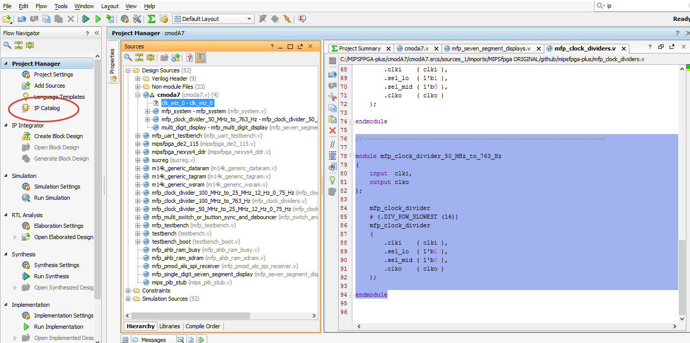
As the processor input receives a signal at 50 MHz which we will create later, if we change the values on the indicator with such a frequency, our eye will not notice these changes (for a normal display of values on the 7th segment indicator, a frequency of approximately 763 Hz is needed) . To do this, connect an instance of the frequency divider:
In the source files, a frequency divider with 50 MHz at 763 Hz is not. Therefore, we will add it to the mfp_clock_dividers.v file:

The system receives the signals reset and clock, RsRx, IO_Buttons. But we have an i_clk signal at the input of the top module, not a clock. The fact is that there is a clock generator at 12 MHz on the board, and the processor in the FPGA can operate at frequencies of 50 MHz and above, and what to do if you have another board with a different clock frequency (for example, Nexys 4 DDR has a clock frequency of 100 MHz). The problem is solved by creating the IP kernel Clocking Wizard (PLL), for this we open the IP directory:
Open the Clocking Wizard:

The board tab is left as it is, or we set up the required inputs and go to the clocking options tab, you can choose either MMCM has a wider input frequency range 10 ... 800 MHz than PLL 19 ... 800 MHz, since on cmoda7 only 12 MHz we choose MMCM, but for other boards you can choose other parameters:

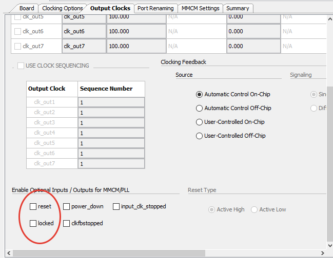
In the output clocks tab, we set the frequency to 50 MHz (you can and should experiment with the frequency, so there may be other characteristics on other FPGAs):

Also remove reset and locked:
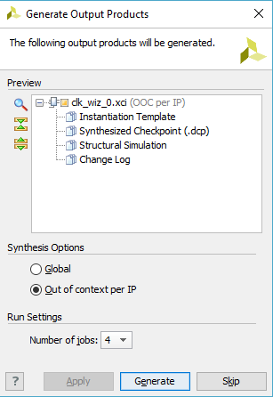
Port renaming, MMCM setting and Summary we look and leave as is, click OK, OK, in the next window choose generate:
We’ll make the last assignment for RGB Led as the final touch, because as you can see from the circuit, they will glow dimly in the floating state, and we want them to be turned off:

At the end write:
The module shell is created, we proceed to change the size of the memory.
The cmoda7 board has 225 KB of block memory. Thus, two blocks of memory (128 Kbytes of RAM of the reset and 256 Kbytes of RAM of the programs) do not fit on the cmoda7 board. Since, the boot code can fit in 32 Kbytes, and you can limit the needs of programs of 64 Kbytes. Thus, the total required memory (32 Kbytes + 64 Kbytes = 96 Kbytes) corresponds to the memory capacity of the cmoda7 board. The remaining 225-96 = 129 Kbytes of memory can be used for other needs of the MIPSfpga system, for example, as a cache memory.
You can reduce the amount of memory by changing the size of the memory stated in the Verilog header file that we connected to the “mfp_ahb_lite_matrix_config.vh” shell. Open the file mipsfpga_ahb_const.vh. Reset RAM addresses (or boot RAM) consist of 13 bits. Thus, the amount of reset RAM is 213 32-bit words = 215 bytes = 32 Kbytes.

Program RAM addresses are 14 bits. Thus, the amount of program RAM is 214 32-bit words = 216 bytes = 64 Kbytes.
Now create a “cmoda7.xdc” which establishes the correspondence between the external signals of the shell module and the cPa7 FPGA case pins ( xdc file with a complete list of pins for cmoda7 ):


For example, the following line establishes the correspondence between the i_clk input and the output of the FPGA L17 chassis, which receives a 12 MHz clock signal from the cmoda7 board.
Also in the file of restrictions you need to add the following output time limits for signals:
We can test the processor ported to our board, for this you need to go to the configuration file "mfp_ahb_lite_matrix_config.vh" and uncomment the line:

Thus, we connected the SPI interface module written on Verilog to the AHB Lite bus for connecting to the PmodALS light sensor from Digilent.

Connection diagram is shown in the picture:
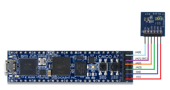
The sensor is connected to the Pmod port, the outputs of which are described in “cmoda7.xdc” are registered as JA [7..0].
The RTL scheme can be explored in the RTL Analisys → Schematic tab, where the SPI interface module "mfp_pmod_als_spi_receiver" is located in the "mfp_system":

To upload the created project to FPGA, you need to generate a bitstream file “cmoda7.bit”, for this, in the tab Program and Debug → Generate Bitstream and wait for the operation to complete:

After creating the bitstream file, you need to load it into the board, for this, in the Program and Debug tab → open the Open Hardware Manager → Open Target → Auto Connect → Program Device and load the system:

In order for the processor to exchange data with the sensor, you need to write a program and load it into a RAM1 block that is also connected to the AHB Lite bus.
The MIPSfpga processor is programmed using Imagination’s Codescape development tools. Install Codescape SDK and OpenOCD. Codescape supports both C and assembly language programming.
To download the code to the system, go to the folder downloaded mipsfpga plus → github → mipsfpga-plus → programs → 01_light_sensor open “mfp_memory_mapped_registers.h”.
next, open main.c and write a couple of lines:
After in the folder we find the script that compiles the code:
Generate the motorola_s_record file:
Check to which COM port the USB UART converter is connected:
Modify the 12_upload_to_the_board_using_uart file:
where a is the number of the COM port to which the USB UART converter is connected. And load the program:
The result of the system porting can be viewed on the video:
To understand the processor, and the possibility of writing new modules in the hardware description language (Verilog, VHDL), as well as circuit design, computer architecture, micro-architecture (organization of the processor pipeline) and programming in assembler, and many other things that will help you start learning It is recommended to read a book of everything related to electronics that is written in the article: Free textbook on electronics, computer architecture and low-level programming in Russian .
The next part will describe how to connect various peripherals to the MIPSfpga system using the example of the Digilent Pmod KYPD keyboard , the built-in ADC, and the LCD display from Nokia.
Porting MIPSfpga to other cards and integrating peripherals into the system. Part 2
This article will describe, using the example of Digilent cmodA7, how to port the MIPSfpga-plus processor to other cards.
')
To date, MIPSFPGA has been ported to popular boards from companies such as ALTERA and Xilinx, among them Basys 3, Nexys4 ddr, and others (the full list is on github ). Such boards are most popular among developers on FPGA. The price of such boards is not quite small, and the programs are loaded into the MIPSfpga core using the EJTAG interface and the Bus Blaster adapter at the cost of about $ 50. The Bus Blaster adapter receives commands via a high-speed USB 2.0 cable and converts them to the serial protocol EJTAG, which allows you to load programs into the MIPSfpga core and control the debugging of the programs that run on it. The problem with relatively expensive Bus Blaster was solved by introducing a number of improvements to the MIPSfpga system. An improved version of the MIPSfpga system, called MIPSfpga-plus, includes such new features:
- Ability to download software using a USB-to-UART connector priced at $ 5 FTDI instead of $ 50 Bus Blaster, which sometimes is not so easy to get.
- The ability to change the clock frequency on the fly from 50 or 25 MHz to 1 Hz (one cycle per second) to monitor the processor in real time, including misses in the cache memory and redirection of the conveyor.
- An example of the integration of the light sensor with the SPI protocol.
- A small software initialization sequence that fits into 1 KB instead of 32 KB of memory, which allows MIPSfpga to be transferred to a wider choice of FPGA cards without using external memory. UART implementation is described in the article: MIPSfpga and UART .
Creating a project in Xilinx Vivado 2016.4 (64 bit) with MIPSfpga-plus
Before adding various peripherals to MIPSfpga +, you need to load and run the system on the FPGA. Some steps of this manual can be skipped if you have a fee from the list below:
Port fees
basys3
de0
de0_cv
de0_nano
de1
de10_lite
de2_115nexys4
nexys4_ddr
de0
de0_cv
de0_nano
de1
de10_lite
de2_115nexys4
nexys4_ddr
MIPSfpga-plus has already been ported to these boards and you can download it at the link:
github.com/MIPSfpga/mipsfpga-plus/tree/master/boards
In another case, if you have a different motherboard from the FPGA listed in the list, it will not be too difficult to port the processor to it. To do this, the following instruction is written, which is shown on the example of my cmodA7 board.
1. First you need to get a package with the MIPSFPGA system. Detailed instructions on how to do this:
→ mipsfpga-download-instruction
You will also need to download the current version of the MIPSfpga-plus extension:
→ Mipsfpga-plus
2. For Xilinx boards, Vivado software is used, the current version can be downloaded at the link:
→ Download Vivado
3. Now let's create a new project in Vivado:
Choose where the created project will be stored:
Click next:
Select the RTL project and click on:
Now add the files of the original MIPSfpga system:
As well as MIPSfpga-plus which are in the archive downloaded from mipsfpga-plus :
Add to the project the uart module that was previously discussed:
Skipping the creation of IP and construction files will create them later:
Next you need to either choose a chip or add your board.
The Digilent cmod A7 board was chosen due to its low price and the presence of the ADC we use later. To select the FPGA scheme, you need to read the documentation on your board, on cmodA7 the xc7a35tcpg236-1 chip is placed:
Another way is to add your board file to the Vivado library, this method is better because, firstly, it is more convenient to remember the name of the board than the chip, and secondly, if you want to use the block designer in Vivado in the future, then you will have additional tools for convenient work with board interfaces, IP cores, etc. You can download them on GitHub , you need to save these files in ~ \ Vivado \ 2015.1 \ data \ boards \ (relevant for Vivado 2015.1 and newer).
So we created a project with MIPSfpga-plus.
Porting Instructions on the example of the Artix-7 based Digilent CmodA7 board
In short, the Artix-7 chip is on board the cmodA7 board, it has 20800 LUT, 41600 FF, 225 KB block memory, 48 pins, 2 of which are ADC outputs, also a usb-uart converter, Quad-SPI Flash, and JTAG, 2 clock buttons, as well as 5 LEDs 3 of which are RGB ( datashit ).
To transfer the MIPSfpga system to the cmodA7 board, you should:
Step 1. Write a shell module that establishes the correspondence between the I / Os of the MIPSfpga and the I / Os of the cmodA7 board.
Step 2. Reduce the memory capacity of the MIPSfpga system to match the cmodA7 board.
Step 3. Add a constraint file that establishes the correspondence between the board I / Os and the FPGA chassis.
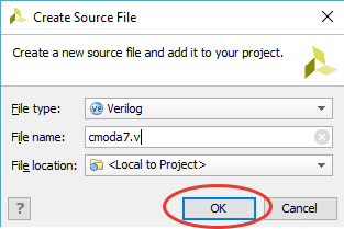
Step 1. Add a new shell file cmoda7.v
Install cmoda7.v as the top module in the system hierarchy.
Since there are no switches on the cmoda7 board that could be used to lower the processor frequency (this modification appeared in MIPSfpga-plus), this module was simply not included in the shell module. You can also exclude the EJTAG output to which the BUS Blaster is connected.
First you need to add the header file for the AHB_lite bus configuration.
`include "mfp_ahb_lite_matrix_config.vh" The Advanced High-Performance Bus (AHB) is an open interface that is used in many microprocessor-based systems, especially embedded ones. AHB bus facilitates the organization of the connection of multiple devices. AHB-Lite is a simplified version of AHB with one master device.
This configuration has one master device, a MIPSfpga processor, and three slaves: RAM0, RAM1, and GPIO, which are (respectively) two blocks of RAM and a module for accessing board I / O devices. We will just work with the GPIO block and write modules for interaction with peripherals.
Let's write the main input-output ports:
module cmoda7 ( input i_clk, input i_btn0, input i_btn1, input RsRx, output [ 6:0] seg, output dp, output [ 3:0] an, output led0_r, output led0_g, output led0_b, inout [ 7:0] JA ); i_clk is the signal of the clock generator of the board frequency (for cmodA7 12 MHz).
i_btn0 - the button is used to reset the processor.
i_btn1 - n / c.
RsRx - receive signal by uart.
seg, dp, an, - contacts for connecting a seven-segment 4-digit indicator.
led_r, led_g, led_b, - the conclusions of the RGB Led placed on the board.
JA - Pmod interface.
The main signals are the clock signal and reset (i_btn0) others for connecting peripherals.
The main purpose of the cmoda7.v module is to create an instance of the MIPSfpga-plus system (mipsfpga_sys) and its connection to the I / O of the board.
wire clock; wire reset = i_btn0; wire display_clock; wire [7:0] anodes; wire [`MFP_N_BUTTONS - 1:0] IO_Buttons; wire [`MFP_7_SEGMENT_HEX_WIDTH - 1:0] IO_7_SegmentHEX; assign IO_Buttons = { { `MFP_N_BUTTONS - 2 { 1'b0 } } , i_btn0, i_btn1 }; mfp_system mfp_system ( .SI_ClkIn ( clock ), .SI_Reset ( reset ), .HADDR ( ), .HRDATA ( ), .HWDATA ( ), .HWRITE ( ), .EJ_TRST_N_probe ( ), .EJ_TDI ( ), .EJ_TDO ( ), .EJ_TMS ( ), .EJ_TCK ( ), .SI_ColdReset ( ), .EJ_DINT ( 1'b0 ), .IO_Switches ( ), .IO_Buttons ( IO_Buttons ), .IO_RedLEDs ( ), .IO_GreenLEDs ( ), .IO_7_SegmentHEX ( IO_7_SegmentHEX ), `ifdef MFP_DEMO_LIGHT_SENSOR .SPI_CS ( JA [0] ), .SPI_SCK ( JA [3] ), .SPI_SDO ( JA [2] ), `endif .UART_RX ( RsRx ), .UART_TX ( ) ); `ifdef MFP_DEMO_LIGHT_SENSOR assign JA [1] = 1'b0; `endif MFP_DEMO_LIGHT_SENSOR will be used when testing a ported system. As you can see, at the output of the mfp_system system there will be a 32-bit IO_7_SegmentHEX bus which we output to the 4-digit 7 segment indicator decoder module, we will wrap the module of the instance “mfp_multi_digit_display”:
mfp_multi_digit_display multi_digit_display ( .clock ( display_clock ), .resetn ( ~ reset ), .number ( IO_7_SegmentHEX ), .seven_segments ( seg ), .dot ( dp ), .anodes ( an ) ); When creating a decoder, it is worth knowing whether the indicator is with a common anode or cathode.
The code of the seven-segment indicator decoder with a common anode has the following form:
module mfp_single_digit_seven_segment_display ( input [3:0] digit, output reg [6:0] seven_segments ); always @* case (digit) 'h0: seven_segments = 'b1000000; // abcdefg 'h1: seven_segments = 'b1111001; 'h2: seven_segments = 'b0100100; // --a-- 'h3: seven_segments = 'b0110000; // | | 'h4: seven_segments = 'b0011001; // fb 'h5: seven_segments = 'b0010010; // | | 'h6: seven_segments = 'b0000010; // --g-- 'h7: seven_segments = 'b1111000; // | | 'h8: seven_segments = 'b0000000; // ec 'h9: seven_segments = 'b0011000; // | | 'ha: seven_segments = 'b0001000; // --d-- 'hb: seven_segments = 'b0000011; 'hc: seven_segments = 'b1000110; 'hd: seven_segments = 'b0100001; 'he: seven_segments = 'b0000110; 'hf: seven_segments = 'b0001110; endcase endmodule //-------------------------------------------------------------------- module mfp_multi_digit_display ( input clock, input resetn, input [31:0] number, output reg [ 6:0] seven_segments, output reg dot, output reg [ 7:0] anodes ); function [6:0] bcd_to_seg (input [3:0] bcd); case (bcd) 'h0: bcd_to_seg = 'b1000000; // abcdefg 'h1: bcd_to_seg = 'b1111001; 'h2: bcd_to_seg = 'b0100100; // --a-- 'h3: bcd_to_seg = 'b0110000; // | | 'h4: bcd_to_seg = 'b0011001; // fb 'h5: bcd_to_seg = 'b0010010; // | | 'h6: bcd_to_seg = 'b0000010; // --g-- 'h7: bcd_to_seg = 'b1111000; // | | 'h8: bcd_to_seg = 'b0000000; // ec 'h9: bcd_to_seg = 'b0010000; // | | 'ha: bcd_to_seg = 'b0001000; // --d-- 'hb: bcd_to_seg = 'b0000011; 'hc: bcd_to_seg = 'b1000110; 'hd: bcd_to_seg = 'b0100001; 'he: bcd_to_seg = 'b0000110; 'hf: bcd_to_seg = 'b0001110; endcase endfunction reg [2:0] i; always @ (posedge clock or negedge resetn) begin if (! resetn) begin seven_segments <= bcd_to_seg (0); dot <= 0; anodes <= 8'b00000001; i <= 0; end else begin seven_segments <= bcd_to_seg (number [i * 4 +: 4]); dot <= 0; anodes <= (1 << i); i <= i + 1; end end endmodule As you can see on each leading edge of the clock in seven_segments, the corresponding signal bcd_to_seg is output, and switching between the indicator bits is performed by switching the active signal on the corresponding anodes (or cathodes).
As the processor input receives a signal at 50 MHz which we will create later, if we change the values on the indicator with such a frequency, our eye will not notice these changes (for a normal display of values on the 7th segment indicator, a frequency of approximately 763 Hz is needed) . To do this, connect an instance of the frequency divider:
mfp_clock_divider_50_MHz_to_763_Hz mfp_clock_divider_50_MHz_to_763_Hz (clock, display_clock); In the source files, a frequency divider with 50 MHz at 763 Hz is not. Therefore, we will add it to the mfp_clock_dividers.v file:
module mfp_clock_divider_50_MHz_to_763_Hz ( input clki, output clko ); mfp_clock_divider # (.DIV_POW_SLOWEST (16)) mfp_clock_divider ( .clki ( clki ), .sel_lo ( 1'b1 ), .sel_mid ( 1'b0 ), .clko ( clko ) ); endmodule The system receives the signals reset and clock, RsRx, IO_Buttons. But we have an i_clk signal at the input of the top module, not a clock. The fact is that there is a clock generator at 12 MHz on the board, and the processor in the FPGA can operate at frequencies of 50 MHz and above, and what to do if you have another board with a different clock frequency (for example, Nexys 4 DDR has a clock frequency of 100 MHz). The problem is solved by creating the IP kernel Clocking Wizard (PLL), for this we open the IP directory:
Open the Clocking Wizard:
The board tab is left as it is, or we set up the required inputs and go to the clocking options tab, you can choose either MMCM has a wider input frequency range 10 ... 800 MHz than PLL 19 ... 800 MHz, since on cmoda7 only 12 MHz we choose MMCM, but for other boards you can choose other parameters:
In the output clocks tab, we set the frequency to 50 MHz (you can and should experiment with the frequency, so there may be other characteristics on other FPGAs):
Also remove reset and locked:
Port renaming, MMCM setting and Summary we look and leave as is, click OK, OK, in the next window choose generate:
We’ll make the last assignment for RGB Led as the final touch, because as you can see from the circuit, they will glow dimly in the floating state, and we want them to be turned off:
assign led0_r = 1'b1; assign led0_g = 1'b1; assign led0_b = 1'b1; At the end write:
endmodule The module shell is created, we proceed to change the size of the memory.
Step 2. Reduce the memory capacity of the MIPSfpga system to match the cmoda7 board
The cmoda7 board has 225 KB of block memory. Thus, two blocks of memory (128 Kbytes of RAM of the reset and 256 Kbytes of RAM of the programs) do not fit on the cmoda7 board. Since, the boot code can fit in 32 Kbytes, and you can limit the needs of programs of 64 Kbytes. Thus, the total required memory (32 Kbytes + 64 Kbytes = 96 Kbytes) corresponds to the memory capacity of the cmoda7 board. The remaining 225-96 = 129 Kbytes of memory can be used for other needs of the MIPSfpga system, for example, as a cache memory.
You can reduce the amount of memory by changing the size of the memory stated in the Verilog header file that we connected to the “mfp_ahb_lite_matrix_config.vh” shell. Open the file mipsfpga_ahb_const.vh. Reset RAM addresses (or boot RAM) consist of 13 bits. Thus, the amount of reset RAM is 213 32-bit words = 215 bytes = 32 Kbytes.
`define H_RAM_RESET_ADDR_WIDTH 13 Program RAM addresses are 14 bits. Thus, the amount of program RAM is 214 32-bit words = 216 bytes = 64 Kbytes.
`define H_RAM_ADDR_WIDTH 14 Step 3. Create the cmoda7 restriction file
Now create a “cmoda7.xdc” which establishes the correspondence between the external signals of the shell module and the cPa7 FPGA case pins ( xdc file with a complete list of pins for cmoda7 ):
## Clock signal 12 MHz set_property -dict {PACKAGE_PIN L17 IOSTANDARD LVCMOS33} [get_ports i_clk] create_clock -period 83.330 -name sys_clk_pin -waveform {0.000 41.660} -add [get_ports i_clk] ## Buttons set_property -dict {PACKAGE_PIN A18 IOSTANDARD LVCMOS33} [get_ports i_btn0] set_property -dict {PACKAGE_PIN B18 IOSTANDARD LVCMOS33} [get_ports i_btn1] ## LEDs set_property -dict {PACKAGE_PIN B17 IOSTANDARD LVCMOS33} [get_ports led0_b] set_property -dict {PACKAGE_PIN B16 IOSTANDARD LVCMOS33} [get_ports led0_g] set_property -dict {PACKAGE_PIN C17 IOSTANDARD LVCMOS33} [get_ports led0_r] ## Pmod Header JA set_property -dict {PACKAGE_PIN G17 IOSTANDARD LVCMOS33} [get_ports {JA[0]}] set_property -dict {PACKAGE_PIN G19 IOSTANDARD LVCMOS33} [get_ports {JA[1]}] set_property -dict {PACKAGE_PIN N18 IOSTANDARD LVCMOS33} [get_ports {JA[2]}] set_property -dict {PACKAGE_PIN L18 IOSTANDARD LVCMOS33} [get_ports {JA[3]}] set_property -dict {PACKAGE_PIN H17 IOSTANDARD LVCMOS33} [get_ports {JA[4]}] set_property -dict {PACKAGE_PIN H19 IOSTANDARD LVCMOS33} [get_ports {JA[5]}] set_property -dict {PACKAGE_PIN J19 IOSTANDARD LVCMOS33} [get_ports {JA[6]}] set_property -dict {PACKAGE_PIN K18 IOSTANDARD LVCMOS33} [get_ports {JA[7]}] ## GPIO Pins 1 - 6 7_segment_ind set_property -dict {PACKAGE_PIN M3 IOSTANDARD LVCMOS33} [get_ports {seg[1]}] set_property -dict {PACKAGE_PIN L3 IOSTANDARD LVCMOS33} [get_ports {an[1]} ] set_property -dict {PACKAGE_PIN A16 IOSTANDARD LVCMOS33}[get_ports {an[2]} ] set_property -dict {PACKAGE_PIN K3 IOSTANDARD LVCMOS33} [get_ports {seg[5]}] set_property -dict {PACKAGE_PIN C15 IOSTANDARD LVCMOS33}[get_ports {seg[0]}] set_property -dict {PACKAGE_PIN H1 IOSTANDARD LVCMOS33} [get_ports {an[3]} ] ## GPIO Pins 43 - 48 7_segment_ind set_property -dict {PACKAGE_PIN U3 IOSTANDARD LVCMOS33} [get_ports {seg[3]}] set_property -dict {PACKAGE_PIN W6 IOSTANDARD LVCMOS33} [get_ports {seg[4]}] set_property -dict {PACKAGE_PIN U7 IOSTANDARD LVCMOS33} [get_ports dp ] set_property -dict {PACKAGE_PIN W7 IOSTANDARD LVCMOS33} [get_ports {seg[2]}] set_property -dict {PACKAGE_PIN U8 IOSTANDARD LVCMOS33} [get_ports {seg[6]}] set_property -dict {PACKAGE_PIN V8 IOSTANDARD LVCMOS33} [get_ports {an[0]} ] ## UART #set_property -dict { PACKAGE_PIN J18 IOSTANDARD LVCMOS33 } [get_ports { uart_rxd_out }]; #IO_L7N_T1_D10_14 Sch=uart_rxd_out set_property -dict {PACKAGE_PIN J17 IOSTANDARD LVCMOS33} [get_ports RsRx] For example, the following line establishes the correspondence between the i_clk input and the output of the FPGA L17 chassis, which receives a 12 MHz clock signal from the cmoda7 board.
set_property -dict {PACKAGE_PIN L17 IOSTANDARD LVCMOS33} [get_ports i_clk] create_clock -period 83.330 -name sys_clk_pin -waveform {0.000 41.660} -add [get_ports i_clk] Also in the file of restrictions you need to add the following output time limits for signals:
# I/O virtual clock create_clock -period 83.330 -name "clk_virt" # tsu/th constraints set_input_delay -clock "clk_virt" -min -add_delay 0.000 [get_ports i_btn0] set_input_delay -clock "clk_virt" -max -add_delay 10.000 [get_ports i_btn0] set_input_delay -clock "clk_virt" -min -add_delay 0.000 [get_ports i_btn1] set_input_delay -clock "clk_virt" -max -add_delay 10.000 [get_ports i_btn1] set_input_delay -clock "clk_virt" -min -add_delay 0.000 [get_ports led0_b] set_input_delay -clock "clk_virt" -max -add_delay 10.000 [get_ports led0_b] set_input_delay -clock "clk_virt" -min -add_delay 0.000 [get_ports led0_g] set_input_delay -clock "clk_virt" -max -add_delay 10.000 [get_ports led0_g] set_input_delay -clock "clk_virt" -min -add_delay 0.000 [get_ports led0_r] set_input_delay -clock "clk_virt" -max -add_delay 10.000 [get_ports led0_r] ## PMOD ALS set_output_delay -clock "clk_virt" -min -add_delay 0.000 [get_ports {JA[0]}] set_output_delay -clock "clk_virt" -max -add_delay 10.000 [get_ports {JA[0]}] set_output_delay -clock "clk_virt" -min -add_delay 0.000 [get_ports {JA[1]}] set_output_delay -clock "clk_virt" -max -add_delay 10.000 [get_ports {JA[1]}] set_input_delay -clock "clk_virt" -min -add_delay 0.000 [get_ports {JA[2]}] set_input_delay -clock "clk_virt" -max -add_delay 10.000 [get_ports {JA[2]}] set_output_delay -clock "clk_virt" -min -add_delay 0.000 [get_ports {JA[3]}] set_output_delay -clock "clk_virt" -max -add_delay 10.000 [get_ports {JA[3]}] set_input_delay -clock "clk_virt" -min -add_delay 0.000 [get_ports {seg[*]}] set_input_delay -clock "clk_virt" -max -add_delay 10.000 [get_ports {seg[*]}] set_input_delay -clock "clk_virt" -min -add_delay 0.000 [get_ports {an[*]}] set_input_delay -clock "clk_virt" -max -add_delay 10.000 [get_ports {an[*]}] set_input_delay -clock "clk_virt" -min -add_delay 0.000 [get_ports dp] set_input_delay -clock "clk_virt" -max -add_delay 10.000 [get_ports dp] set_output_delay -clock "clk_virt" -min -add_delay 0.000 [get_ports RsRx] set_output_delay -clock "clk_virt" -max -add_delay 10.000 [get_ports RsRx] MIPSfpga test
We can test the processor ported to our board, for this you need to go to the configuration file "mfp_ahb_lite_matrix_config.vh" and uncomment the line:
`define MFP_DEMO_LIGHT_SENSOR Thus, we connected the SPI interface module written on Verilog to the AHB Lite bus for connecting to the PmodALS light sensor from Digilent.
SPI module
module mfp_pmod_als_spi_receiver ( input clock, input reset_n, output cs, output sck, input sdo, output reg [15:0] value ); reg [21:0] cnt; reg [15:0] shift; always @ (posedge clock or negedge reset_n) begin if (! reset_n) cnt <= 22'b100; else cnt <= cnt + 22'b1; end assign sck = ~ cnt [3]; assign cs = cnt [8]; wire sample_bit = ( cs == 1'b0 && cnt [3:0] == 4'b1111 ); wire value_done = ( cnt [21:0] == 22'b0 ); always @ (posedge clock or negedge reset_n) begin if (! reset_n) begin shift <= 16'h0000; value <= 16'h0000; end else if (sample_bit) begin shift <= (shift << 1) | sdo; end else if (value_done) begin value <= shift; end end endmodule Connection diagram is shown in the picture:
The sensor is connected to the Pmod port, the outputs of which are described in “cmoda7.xdc” are registered as JA [7..0].
## Pmod Header JA set_property -dict {PACKAGE_PIN G17 IOSTANDARD LVCMOS33} [get_ports {JA[0]}] ... set_property -dict {PACKAGE_PIN K18 IOSTANDARD LVCMOS33} [get_ports {JA[7]}] The RTL scheme can be explored in the RTL Analisys → Schematic tab, where the SPI interface module "mfp_pmod_als_spi_receiver" is located in the "mfp_system":
To upload the created project to FPGA, you need to generate a bitstream file “cmoda7.bit”, for this, in the tab Program and Debug → Generate Bitstream and wait for the operation to complete:
After creating the bitstream file, you need to load it into the board, for this, in the Program and Debug tab → open the Open Hardware Manager → Open Target → Auto Connect → Program Device and load the system:
Download programs for working with the sensor
In order for the processor to exchange data with the sensor, you need to write a program and load it into a RAM1 block that is also connected to the AHB Lite bus.
The MIPSfpga processor is programmed using Imagination’s Codescape development tools. Install Codescape SDK and OpenOCD. Codescape supports both C and assembly language programming.
To download the code to the system, go to the folder downloaded mipsfpga plus → github → mipsfpga-plus → programs → 01_light_sensor open “mfp_memory_mapped_registers.h”.
#define MFP_LIGHT_SENSOR_ADDR 0xBF800014 #define MFP_LIGHT_SENSOR (* (volatile unsigned *) MFP_LIGHT_SENSOR_ADDR ) next, open main.c and write a couple of lines:
#include "mfp_memory_mapped_registers.h" int main () { int n = 0; for (;;) { MFP_7_SEGMENT_HEX = MFP_LIGHT_SENSOR; } return 0; } After in the folder we find the script that compiles the code:
02_compile_and_link Generate the motorola_s_record file:
08_generate_motorola_s_record_file Check to which COM port the USB UART converter is connected:
11_check_which_com_port_is_used Modify the 12_upload_to_the_board_using_uart file:
set a=7 mode com%a% baud=115200 parity=n data=8 stop=1 to=off xon=off odsr=off octs=off dtr=off rts=off idsr=off type program.rec >\.\COM%a% where a is the number of the COM port to which the USB UART converter is connected. And load the program:
12_upload_to_the_board_using_uart The result of the system porting can be viewed on the video:
To understand the processor, and the possibility of writing new modules in the hardware description language (Verilog, VHDL), as well as circuit design, computer architecture, micro-architecture (organization of the processor pipeline) and programming in assembler, and many other things that will help you start learning It is recommended to read a book of everything related to electronics that is written in the article: Free textbook on electronics, computer architecture and low-level programming in Russian .
The next part will describe how to connect various peripherals to the MIPSfpga system using the example of the Digilent Pmod KYPD keyboard , the built-in ADC, and the LCD display from Nokia.
Porting MIPSfpga to other cards and integrating peripherals into the system. Part 2
Source: https://habr.com/ru/post/329808/
All Articles