BK-0010 emulator on FPGA - part 2
First part
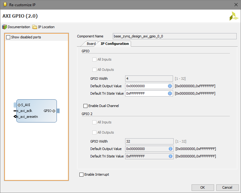
If you have already managed to work with the block design in Vivado, then you could see that the appearance of many standard IP changes depending on the settings that are configured. For example, the AXI-GPIO module can be single-channel or two-channel, depending on the “Enable dual channel” parameter:
 |  |
For the BK-0010 project, it will also be convenient for us to use this technology and today we will learn how to do it.
Also in this part we:
- Consider a general information about the architecture of the BK-0010
- Let's talk about interfaces, how to create them and how to work with them.
- Create a few auxiliary IP, the appearance and characteristics of which vary depending on the parameters.
Architecture Overview
All elements of the -0010 (CPU, RAM, ROM, ports) are interconnected via the MPD bus. MPI is a simplified version of the Q-bus from DEC, it is a 16-bit combined (the address and data are transmitted over the same conductors) bidirectional bus.
')
The original MPI bus was asynchronous, some signals were exposed on it with some delays normalized to nanoseconds.
In the event that the Slave device did not respond for too long in the bus exchange process over the DIM, a bus error interrupt occurred (unlike, for example, the Z80, where there was nothing like this). This architectural feature is used in BK-0010, so it needs to be emulated.
In the project BK-0010, a similar internal bus will be used. Of course, there is no point in doing a combined bidirectional address bus and data inside the FPGA, so there will be three buses - ADDR, DATAIN, DATAOUT (all 16 bits each). The tire will be completely synchronous, no delays in nanoseconds.
In BK-0010, there was only one Master device on the MPI bus — the CPU; therefore, I did not implement bus capture procedures, direct memory access, and the like.
I left the rest of the signals as original as possible:
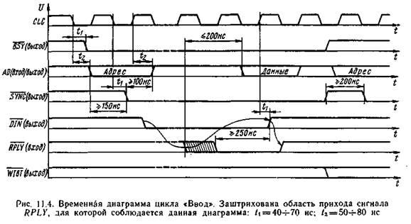
SYNC - A signal indicating that Master has set the address on the ADDR bus. Memory is addressed by bytes, but the data bus bytes with an even address is always transmitted in the lower 8 bits, bytes with an odd in the high.
DIN - A signal indicating that the Master has requested a read at a previously set address. Reading is always done in two-byte words, if the Master only needs one byte, the second is ignored.
DOUT - A signal indicating that the Master has set data to the DATAOUT bus and requires that the data be recorded at a previously set address.
WTBT - A signal indicating that a byte operation is in progress. Exhibited only in the recording cycle. The master is obliged to set the recordable byte either to the lower 8 bits of the DATAOUT bus (in the case of an even address) or to the older ones (in the case of an odd one). The remaining byte is ignored by the Slave device.
RPLY - A signal by which Slave informs the Master that it has completed a bus cycle (set data in a read cycle or received it in a write cycle). If the signal does not arrive within 64 cycles, a bus interrupt occurs.
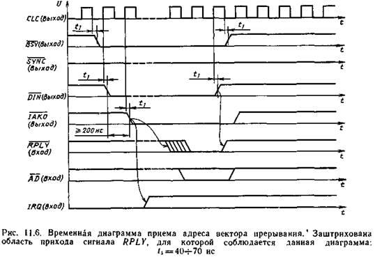
VIRQ - Interrupt request signal.
IAKO - Signal acknowledgment / request address interrupt. This signal passed sequentially through all devices that could require an interrupt. If the device is currently not required to interrupt, then it transmitted a signal further down the chain. If the device is currently demanding an interrupt, then it did not transmit a signal further and began the cycle of transmitting the address of the interruption. The position of the device in the IAKO signal transmission chain determined its relative priority.
Interrupts from external devices in BK-0010 are used, so these signals are needed.
Tires and interfaces
With tires and interfaces, there is some terminological confusion that needs attention. In Verilog / VHDL, a bus (bus) is an associated set of digital signals of the same type designed to transmit multi-digit numbers. For example, a data bus consisting of eight bits.
In addition, the bus is also called the set of heterogeneous signals (signals for data, address, control). For example, a PCI bus, an AXI4 bus, in our case an MPI bus. Such a construction in the terminology of Xilinx Vivado is called an interface.
We will have to work with the MPI bus in several places. This interface will have at least CPU, RAM, ROM, ports of external devices. For convenience, we will make its description as a single entity, so that you do not have to manually connect each signal each time.
To do this, in Vivado, call the Tools-> Create interface tool:
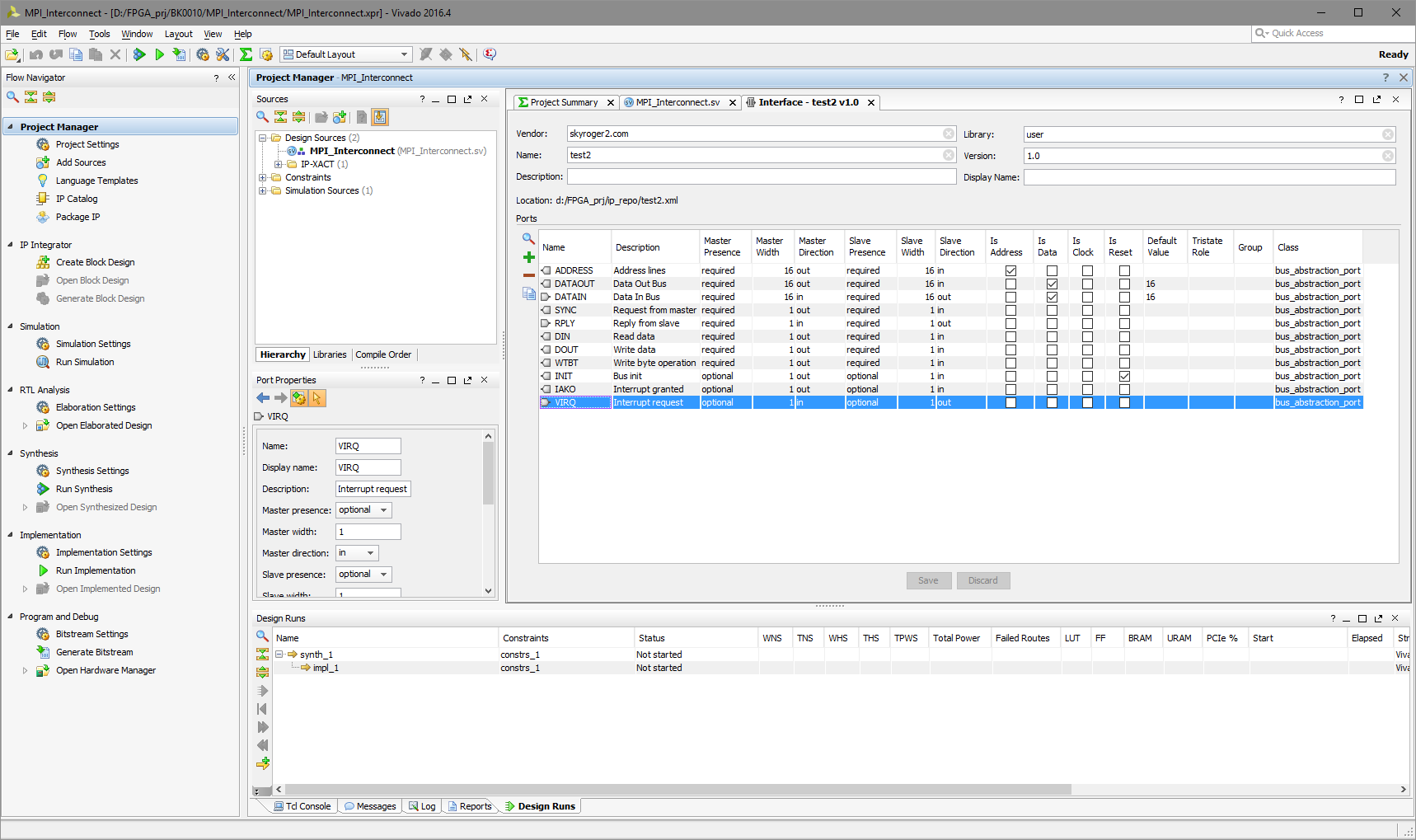
We add here all the necessary signals, indicate their direction (for the Slave, the direction will be automatically inverted compared to the Master), denote which signals must be present and which may be missing. Separately note the sync and reset signals.
Interface description is saved in xml format. In order for us in the project to work with him, it is necessary to add the path to the folder with this file in the project properties.

IP module with customizable features
Consider how to create such modules on the example of interconnect. Interconnect is a module that interconnects Master and Slave ports. Since the number of ports is not known in advance, this parameter should be configurable. The interconnect module itself is very simple in our case, since we do not need any bus width conversion or buffering. It can be implemented on combinational logic.
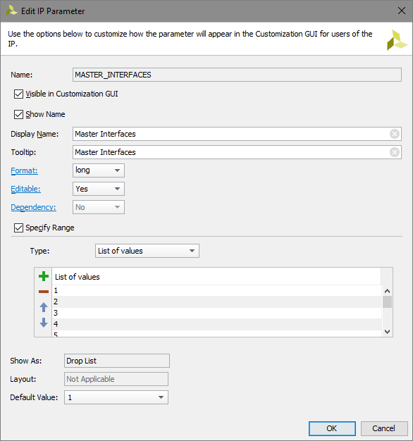
In our case, we will have only one processor, according to the interconnect, it is enough to have only one Slave port. The number of master ports will be set by the parameter MASTER_INTERFACES:

The current revision of the module supports up to 11 Master ports, of course this number can be made by any.
So, create our module
- We create the head file of the module in which we describe all the signals that can come to this module. There will be a lot of them - we need to describe all the signals for all possible MPI ports (1 Slave + 11 Master) + clk and rst signals. So far, the clk and rst signals in the module are not used, since it is entirely based on combinational logic, but I left them for consistency, all of a sudden, in the future, buffering or something similar will be needed.
module MPI_Interconnect ( input [15:0] S00_ADDR, input [15:0] S00_DATA_W, output [15:0] S00_DATA_R, input S00_SYNC, output S00_RPLY, input S00_DIN, input S00_DOUT, input S00_WTBT, input S00_IAKO, output reg S00_VIRQ, output [15:0] M00_ADDR, output [15:0] M00_DATA_W, input [15:0] M00_DATA_R, output M00_SYNC, input M00_RPLY, output M00_DIN, output M00_DOUT, output M00_WTBT, output M00_IAKO, input reg M00_VIRQ, ... - Let's transform our module to IP (Tools-> Create and Package new IP). After that, we have a new item IP in the Project Manager, where you can customize the project settings.
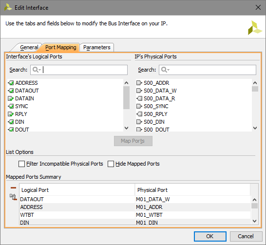
- On the Interfaces tab, we create 12 MPI interfaces using the interface description created in the previous step.
- We configure mapping between the created MPI interfaces and the module signals. If the module signals are named the same as the ports in the interface, then Vivado will make this mapping itself, but in this case it cannot guess that the M00_ADDR and M00_DIN signals belong to the zero Master port, and M02_DOUT to the second one, so something happens touch up.
- Set the list of possible values for the parameter MASTER_INTERFACES. In addition to the list, you can also use the values in hexadecimal or decimal, checkbox, radio button.
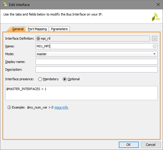
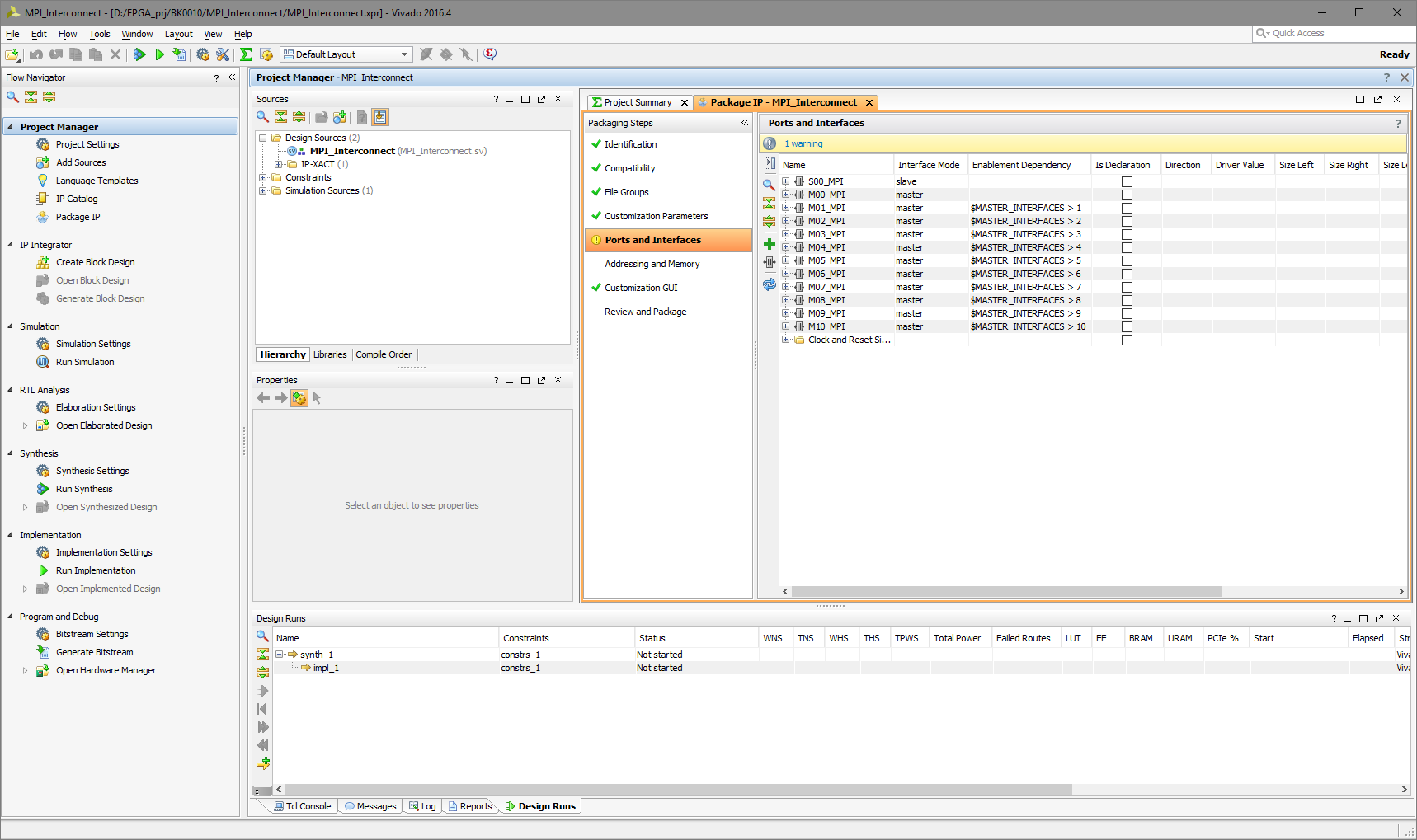
- We configure the conditions of visibility of ports. The S00_MPI and M00_MPI ports are always visible here, we mark the port M01_MPI as optional and that it should be visible only under the condition $ MASTER_INTERFACES> 1. We proceed in the same way with the other Master ports.
- Using the conditional compilation options in Verilog, we create the necessary logic for the operation of our module, depending on the value of the MASTER_INTERFACES parameter:
if (MASTER_INTERFACES > 1) begin assign M01_ADDR = S00_ADDR; assign M01_DATA_W = S00_DATA_W; assign M01_SYNC = S00_SYNC; assign M01_DIN = S00_DIN; assign M01_DOUT = S00_DOUT; assign M01_WTBT = S00_WTBT; assign M01_IAKO = (M00_VIRQ == 1) ? S00_IAKO : 1; end ...
Now, instead of a hundred and fifty signals, we have a neat list of 12 interfaces that we can use in block design:
At this stage, we also create several modules with an MPI interface, these are RAM and ROM modules. Their implementation is rather trivial, based on a finite state machine that implements the logic of the MPI bus, specifically reading cycles (ROM) or reading and writing (RAM). We have three ROM modules — one for the system monitor, the other for the Focal interpreter, and the third for the test module. The size of each module is 8 KB, they are all created on the basis of FPGA block memory. The size of the RAM module is 32KB.
The important point is that namespaces are not supported, so the arrays for initializing different ROM must be called differently. The same name (even in different IP) leads to a difficult-to-diagnose situation when one ROM is initialized with the contents of another, and no warning is given about this.
We start to collect our project. While we have a little - interconnect module and RAM and ROM modules:
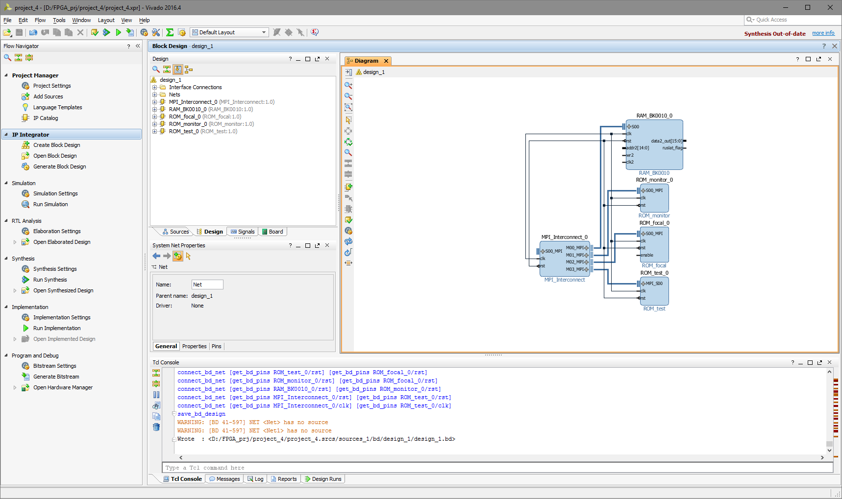
The clk and rst signals are not connected yet, we will connect them as soon as we deal with the clock domains. The RAM module has a lot of unconnected signals left - the display controller will be connected there. On the left, the interconnect has an MPI Slave interface. A CPU module will be connected here.
To be continued.
Links
→ Interface description MPI
→ Interconnect module MPI
→ RAM Module
→ System Monitor ROM Module
→ ROM module interpreter language Focal
→ ROM module of the test subsystem
Source: https://habr.com/ru/post/328148/
All Articles