Revision # 1. The key to start
Hello to all!
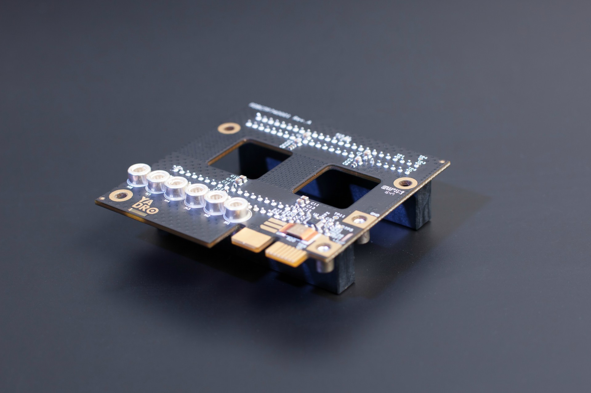
For quite a while there was no news from us — they turned the charts and drawings of the server into real hardware. Now we have a working first revision, and on the eve of the May holidays, you can be pleased with the story, what our developers have been doing for the last six months. And of course, to show the result - in this article for the first time we will publish photos, and not just diagrams and models.
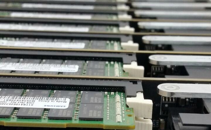
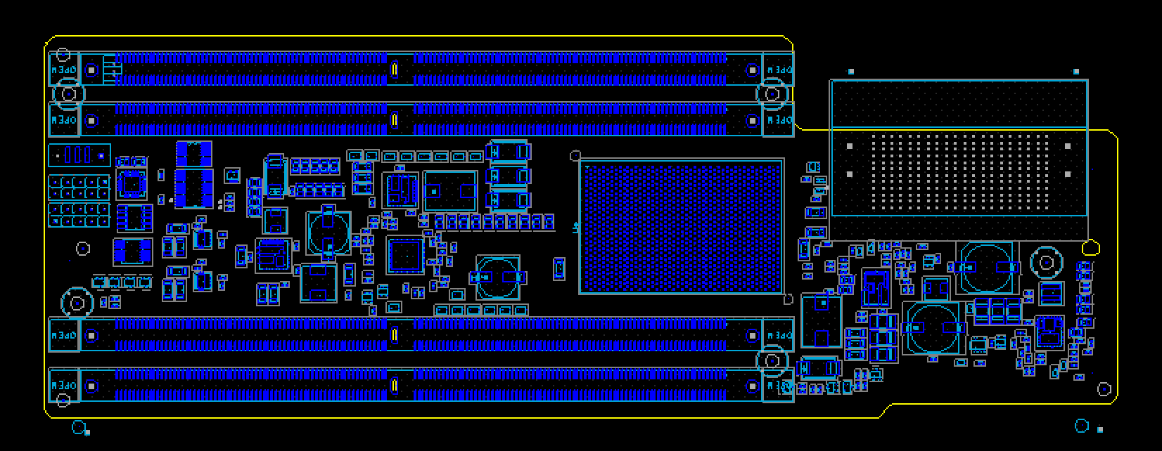
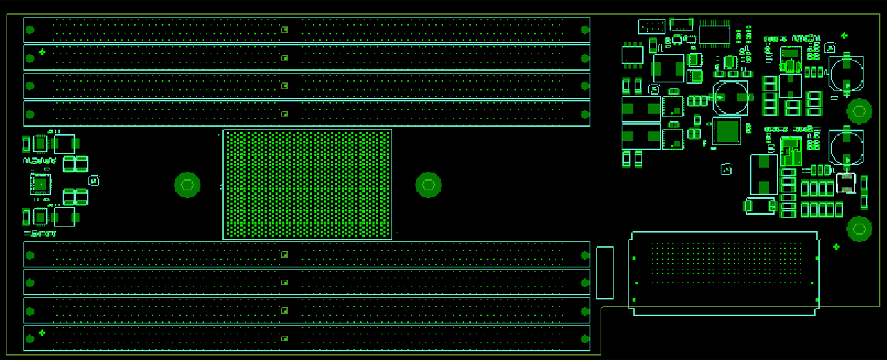
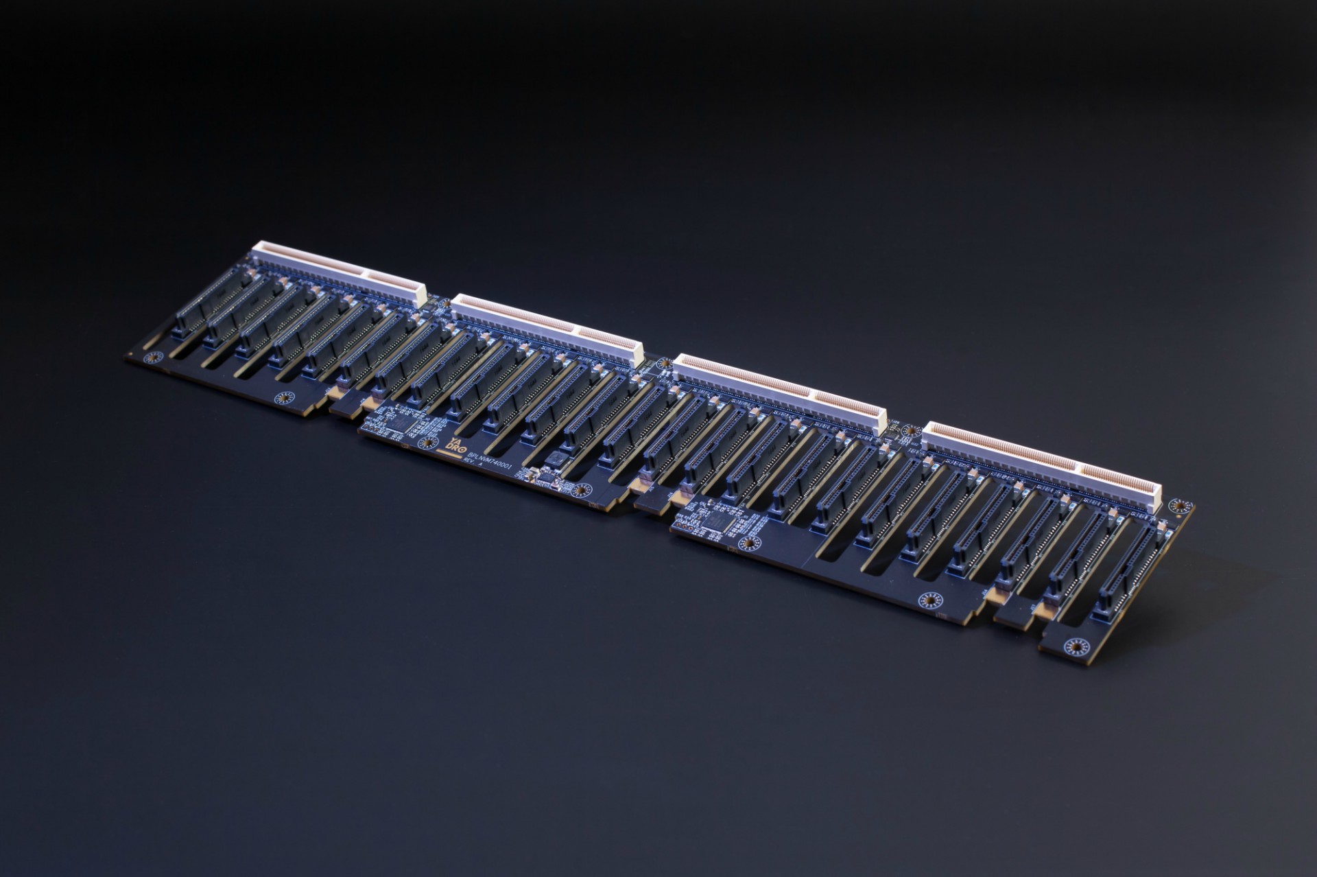
Raisers with memory in the first revision of our server.
We did a lot:
')
Then I will tell you about each topic in turn, and for each I will drop fresh portions of stylish engineering graphics and photos. Thanks to a fellow programmer who is fond of photography for good photos - I took the components off yesterday while there was a break in the iron tests (I had to shoot the picture for the article’s head after he left home).
Since the publication of our introductory article on the motherboard, we have been engaged in the final agreement on all the requirements for the location of power rails and connectors. We also fixed memory riser circuits - they affect pin-out connectors for risers on the motherboard. Approved power distribution board circuits from CRPS-blocks and pinout OCuLink connectors (Nano-Pitch).
On nutrition, it still happened to place and dilute the VRM for the processors on the motherboard - no additional fees were needed. Given the density of the board, the required area of the feeding grounds and the number of vias required for the passage of a large current, we had to tinker. And after that, they fine-tuned high-speed circuits for the best signal quality.
The output was mighty:
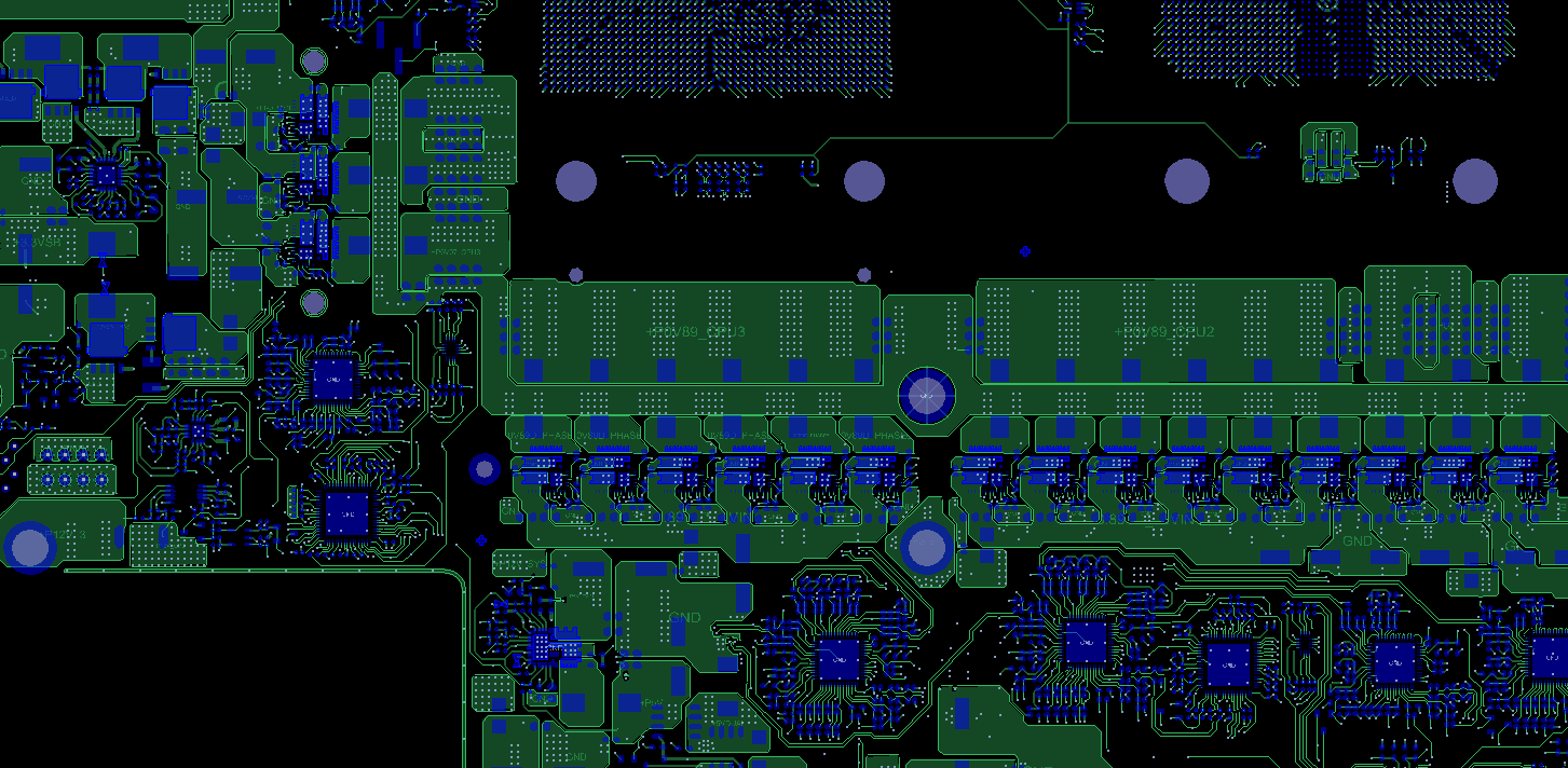
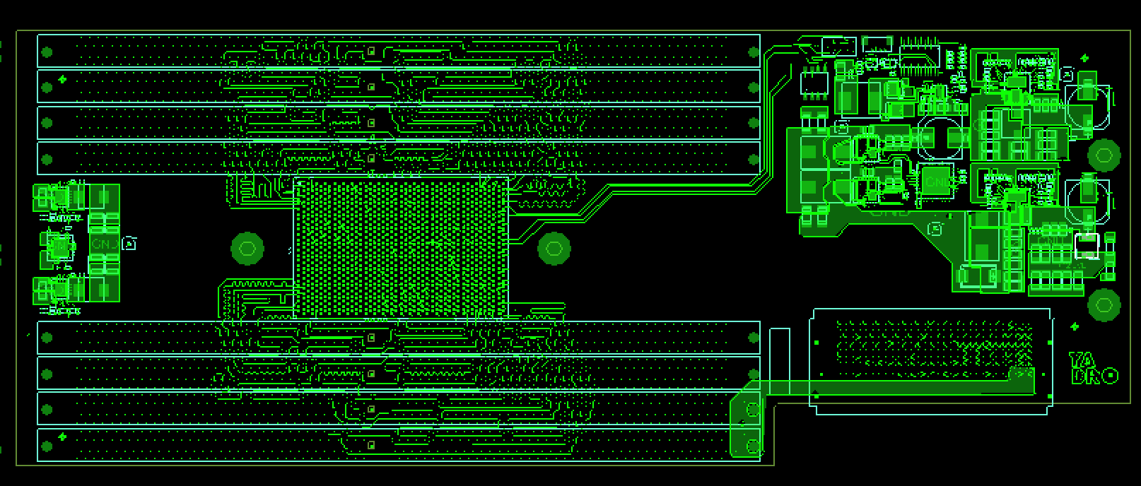
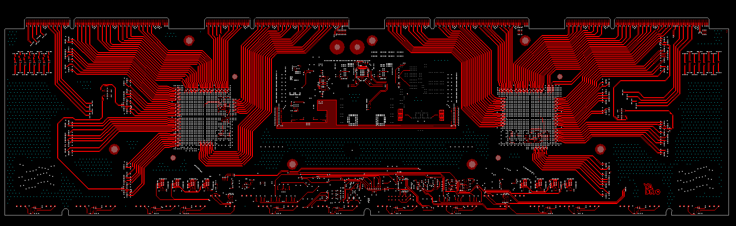
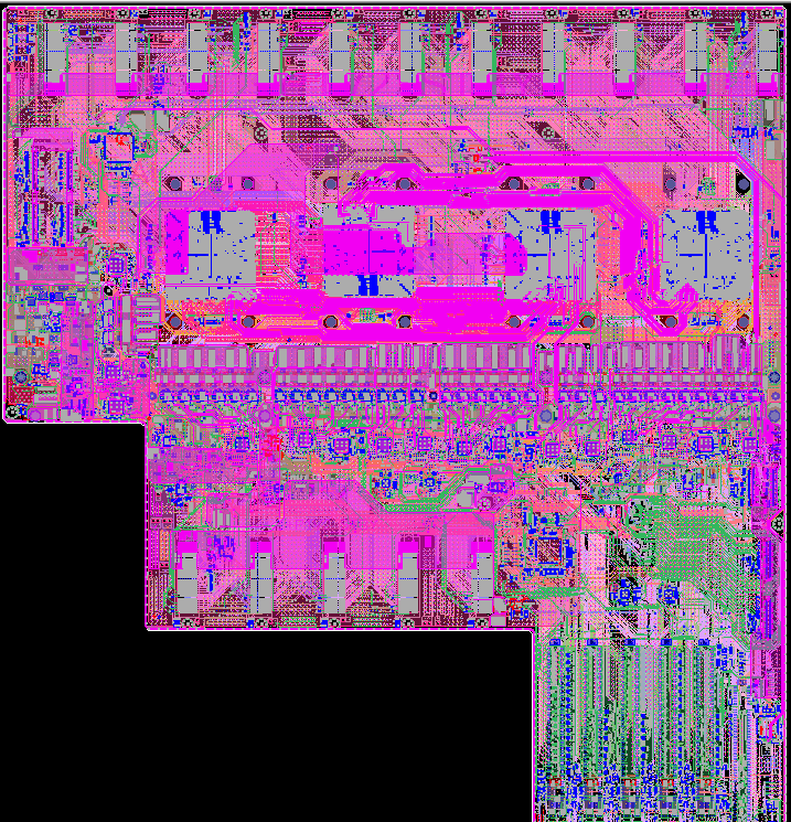 Motherboard server in all merciless for the eyes of beauty.
Somewhere tracing was easier:
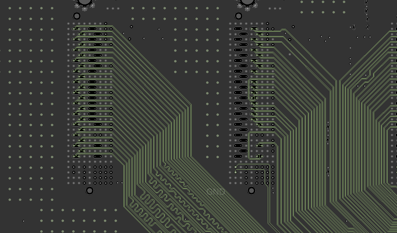 Trace the DMI bus near memory connectors.
Somewhere a bit more complicated:
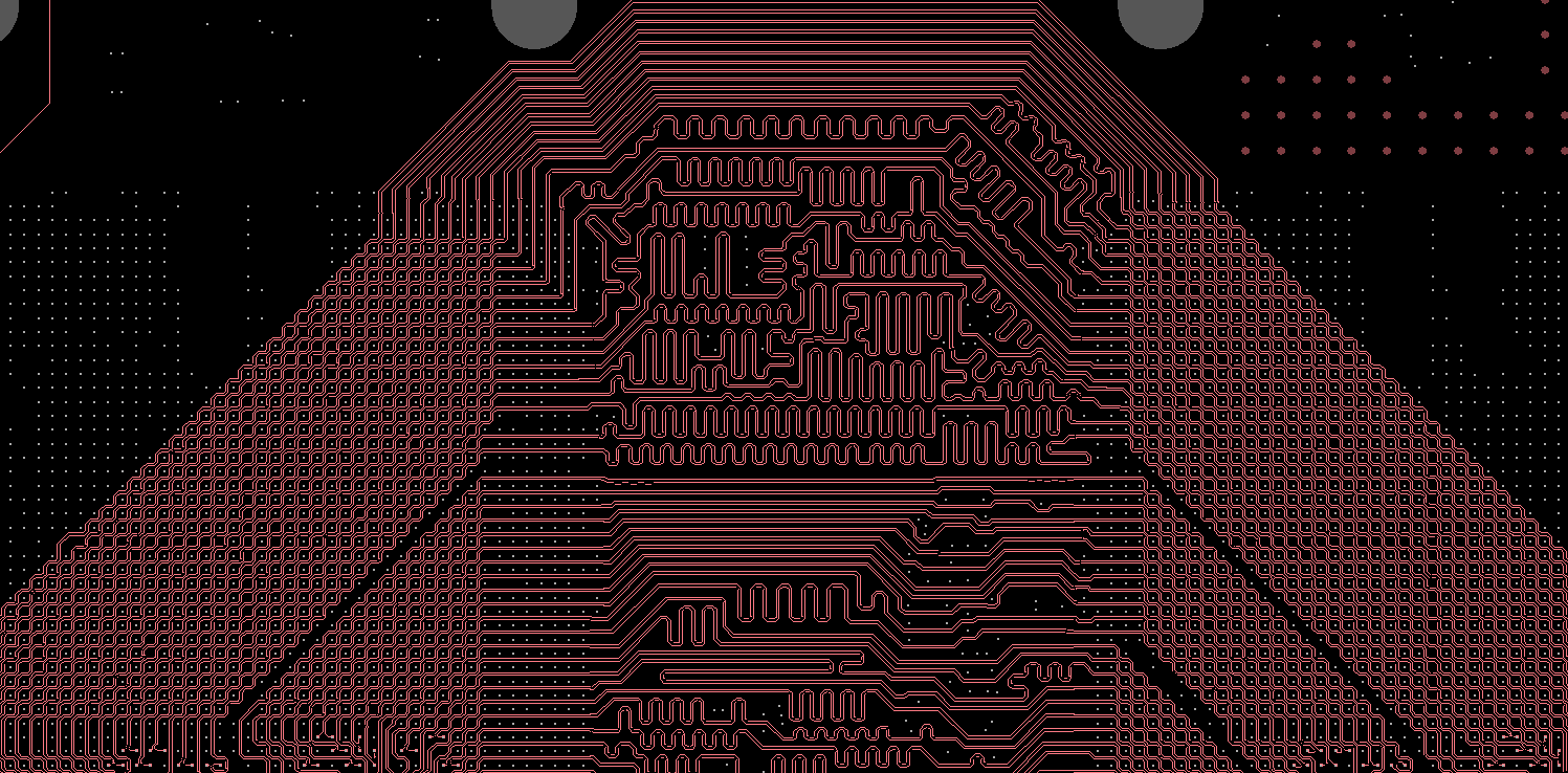 A-Bus tracing between two processors. A bit of dark magic and sleight of hand.
And in this picture you can see how the VRM processors are packed:
 VRM processors in a cohesive series.
And finally, we can show the result of the work on the motherboard. So it looks like after manufacture and installation:
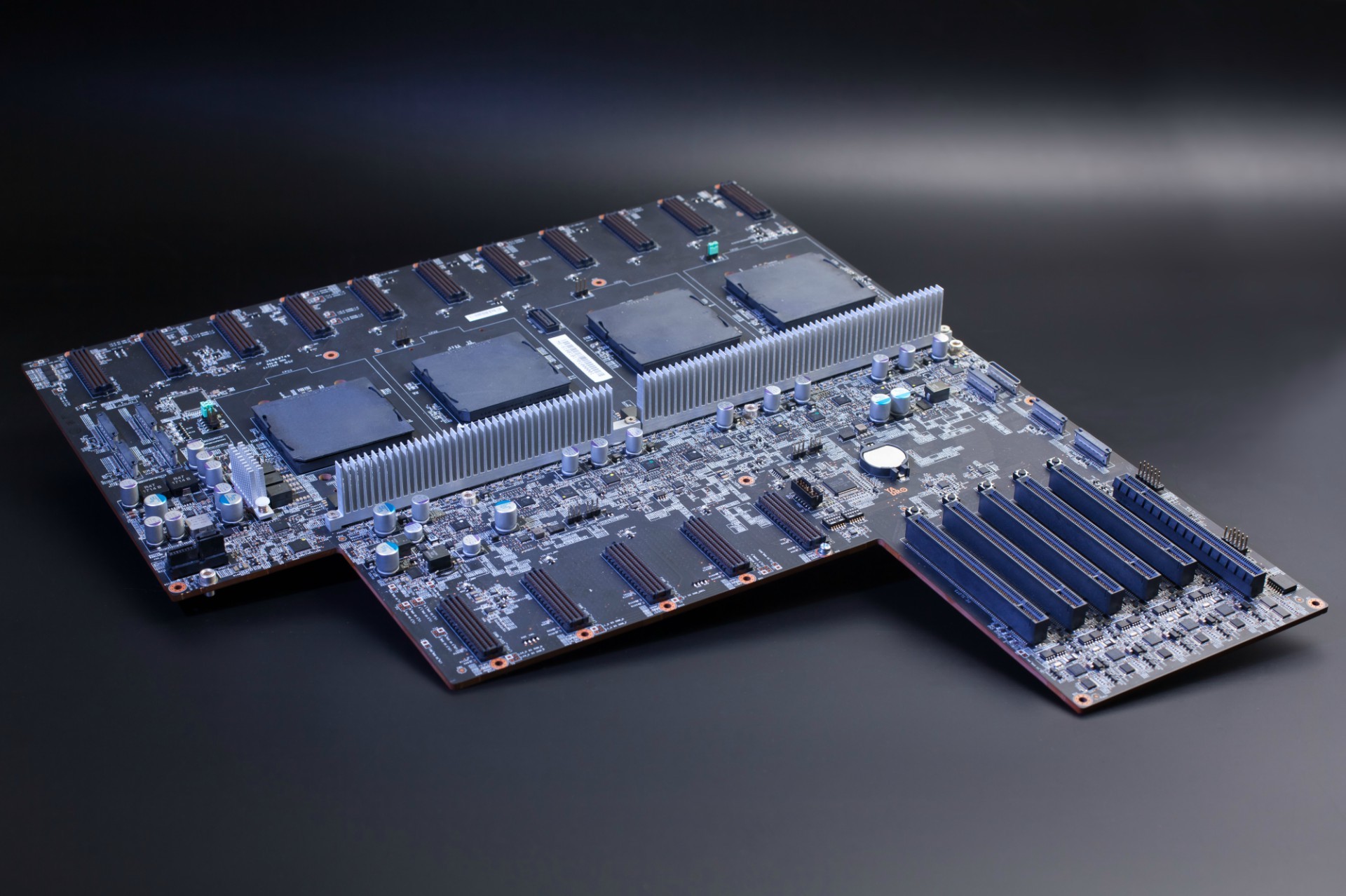 The first revision of the motherboard.
We made the memory riser based on the OpenPOWER reference design. The main difference is that we increased the number of DIMM connectors to two per channel (there was one) with approximately the same board dimensions.
Here are illustrations of the riser from the reference design and ours:
 Reference design riser.
 And this is our riser design.
To accommodate a greater number of connectors, we had to modify the reference design in several directions at once:
During the development of this board, we encountered two main difficulties:
The main problem was with the wiring of the bus address and commands, since when the DIMM and Memory Buffer come together we did not leave room for ourselves to align this bus (it is located in the center of the DIMM socket). To overcome this problem, we carried part of the address bus and commands to the outer layers (in the reference design, all wiring is carried out on the inner layers).
 Riser memory layout.
The speed of propagation of signals on the outer and inner layers is different - therefore, the alignment of this tire we carried out in units of time, not length.
The second problem was that the connector we used did not have an 85-ohm version, only 100 ohm. While a fast DMI bus passing through it has an impedance of 85 ohms.
However, we concluded that due to a drop in impedance on the pads of the connector to approximately 60 ohms, the use of a 100-ohm connector is even more preferable, since it leads to a certain compensation for this irregularity.
Here's what happened in the end:
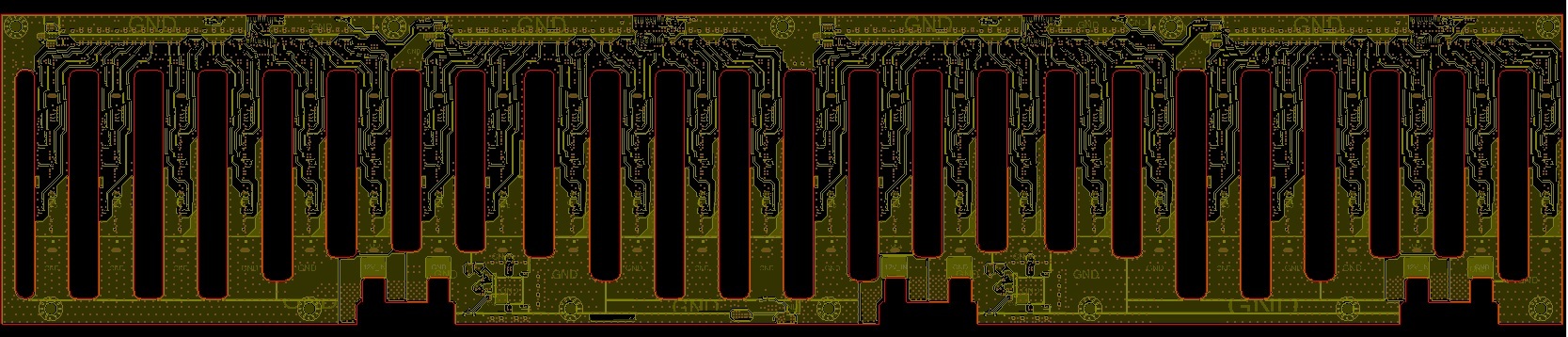
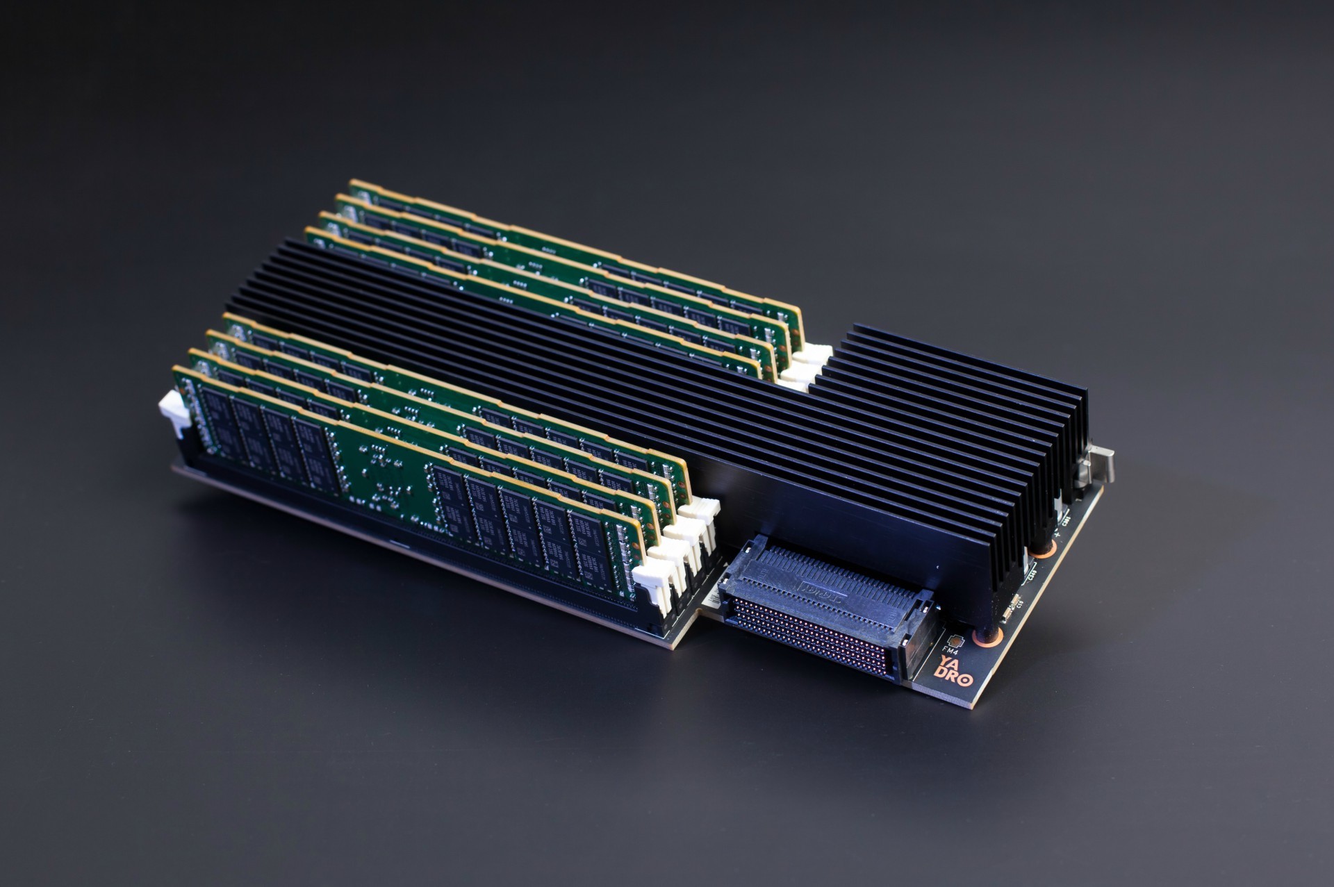 Raiser memory. Under the radiator hides Centaur memory buffer. To save space, use the dense 240-pin Samtec Searay SEAF-RA connectors.
The board with PCIe switches in the server is located above the disks - as it was written in the review article about the server , it’s physically impossible to place them on the backplane, it’s too big chips. They fit under the cover of the server.
There are 2 PCIe switch chips on the board, and each of them in our case can consist of 2 independent parts (partitions). Up to 4 switches in total, and each of them is connected to its processor via a PCIe Gen3 x16 bus. We made these connections with OCuLink cables. If a smaller number of processors are installed in the system, you can reconfigure the partitioning of switches to provide the necessary connection between the disks and the processors.
During development and tracing, we had to take into account many restrictions on the layout of components on the board, caused by stringent height requirements. Due to the fact that there are disk baskets under the board, we could only put passive components of size 0402 on the bottom side of the board. On the upper side we were limited to a height of 9 mm.
I had to think about the relative location of the OCuLink connectors and switches, so that it was more convenient to trace and connect the cables when building the server. The result was the following layout of the components:
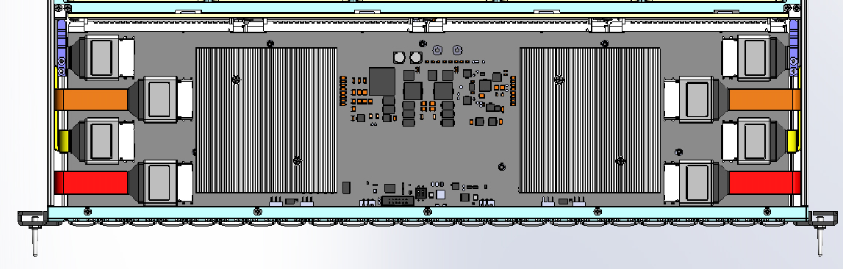
Switch card layout for NVMe disks; below, protruding parts of disk baskets are visible.
This arrangement of chips and connectors required to make a separate configuration file for each of the chips. The switch chips we have chosen have 5 x16 line blocks (chip maker Microsemi calls them stacks), which are divided between two partitions. Due to the fact that for convenience of tracing and installation, the chips are deployed relative to each other, it was convenient to register different lines for different chips to connect to the host and to the NVMe disks. In itself, it does not cause difficulties, but in production it is necessary to ensure that the configuration intended for it has been stitched into each of the two chips.
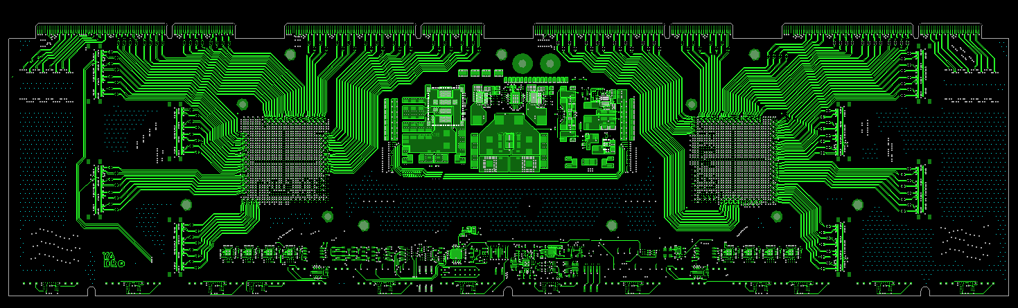 The top layer of the switchboard.
 The bottom layer of the switchboard. Welcome to the dark side.
On the inner side, on the edge of the board, there is a line of edge connectors, through which the board is connected to the disk backplane. And from the front, we placed on it signal LEDs for disks - in this way we simplified the design of disk modules and disk backplane. The board itself is still in production, we will show its photos in the following articles.
Up to 24 NVMe disks are connected to the backplane. Since we carried the disk LEDs onto the switchboard, we did not have to use light guides to display the indications on the front panel. If the LEDs were on the backplane, it would have been impossible to do without 24 long light guides (they are usually placed in the disk tray).
The backplane fee is across the entire server perpendicular to the air flow. To provide good cooling for processors and memory, we had to make many evenly spaced holes in it. We also tried to make the size of the holes larger, increasing the trace density and thinking through the optimal arrangement of the components on the board. But during the tracing, I still had to slightly reduce the size of the slots for high-quality passing high-speed PCIe signals to the disks.
 Diskbackline scheme. Tracks evoke memories of Giger.
Power to the board comes through 3 pairs of powerful pins (RADSOK) - the grounds for them can be clearly seen in the picture below. Power is supplied to the disks, as well as to the switchboard through the edge connectors.
 Disk backplane, view from the side of disk baskets.
Immediately behind the disk backplane in our server are 5 fans. They are placed in the guides and connected to the midplane using small cards that are placed on the fan casing.
In addition to transmitting the control signal to the fans and feedback from them, the fan board distributes power from the CRPS sources to the fans, as well as to the disk backplane. The total current is quite high (up to 75 A at the peak), and the width of the board is not very large, so I had to create a midplein with an increased thickness of copper on the layers. Powered by CRPS sources summed up through copper tires.
 Fans fee. Simple
This is almost the smallest board in the server, but it plays an important role - it removes power from two units and distributes it to the server modules. We decided to transfer power from this board to the rest of the system through copper buses through powerful contacts (RADSOK series).
Standby power is transmitted through the edge connector. Also through this connector are signals for switching on power supply units, “power good” CRPS signals, as well as data from a current sensor, which measures the consumption of disks and fans.
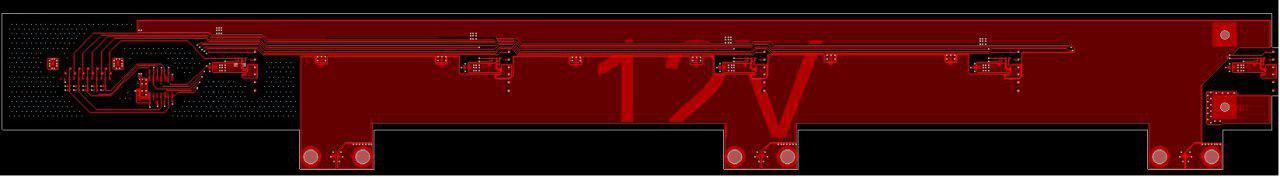
 The power distribution board is small but powerful.
After the May holidays, we will talk in more detail about testing and debugging of various subsystems. Stay tuned!
For quite a while there was no news from us — they turned the charts and drawings of the server into real hardware. Now we have a working first revision, and on the eve of the May holidays, you can be pleased with the story, what our developers have been doing for the last six months. And of course, to show the result - in this article for the first time we will publish photos, and not just diagrams and models.
Raisers with memory in the first revision of our server.
We did a lot:
')
- We completed the tracing and made samples of motherboards, control boards and memory raiser boards.
- We developed and sent to production PCI switch boards, boards for fans and display boards and interfaces (with buttons, connectors and LEDs).
- We developed and launched into production power distribution boards from CRPS sources and backplanes for NVMe disks.
- After the arrival of the first samples, the debugging of the motherboard, the control board and the memory riser went through.
- We finished the server case - during the design of the boards small changes were required in several places.
Then I will tell you about each topic in turn, and for each I will drop fresh portions of stylish engineering graphics and photos. Thanks to a fellow programmer who is fond of photography for good photos - I took the components off yesterday while there was a break in the iron tests (I had to shoot the picture for the article’s head after he left home).
Motherboard
Since the publication of our introductory article on the motherboard, we have been engaged in the final agreement on all the requirements for the location of power rails and connectors. We also fixed memory riser circuits - they affect pin-out connectors for risers on the motherboard. Approved power distribution board circuits from CRPS-blocks and pinout OCuLink connectors (Nano-Pitch).
On nutrition, it still happened to place and dilute the VRM for the processors on the motherboard - no additional fees were needed. Given the density of the board, the required area of the feeding grounds and the number of vias required for the passage of a large current, we had to tinker. And after that, they fine-tuned high-speed circuits for the best signal quality.
The output was mighty:
Motherboard server in all merciless for the eyes of beauty.Somewhere tracing was easier:
Trace the DMI bus near memory connectors.Somewhere a bit more complicated:
A-Bus tracing between two processors. A bit of dark magic and sleight of hand.And in this picture you can see how the VRM processors are packed:
VRM processors in a cohesive series.And finally, we can show the result of the work on the motherboard. So it looks like after manufacture and installation:
The first revision of the motherboard.Memory raiser
We made the memory riser based on the OpenPOWER reference design. The main difference is that we increased the number of DIMM connectors to two per channel (there was one) with approximately the same board dimensions.
Here are illustrations of the riser from the reference design and ours:
Reference design riser. And this is our riser design.To accommodate a greater number of connectors, we had to modify the reference design in several directions at once:
- Replaced SMD DIMM connectors with Press-Fit, since they can be placed much closer to each other.
- DIMM slots are brought closer to the memory buffer chip.
- Threw out of the circuit many debug connectors.
- Optimized power subsystem schematics to reduce the area occupied by the components.
- Used a more dense connector to connect to the motherboard.
During the development of this board, we encountered two main difficulties:
1. Layout has become more dense
The main problem was with the wiring of the bus address and commands, since when the DIMM and Memory Buffer come together we did not leave room for ourselves to align this bus (it is located in the center of the DIMM socket). To overcome this problem, we carried part of the address bus and commands to the outer layers (in the reference design, all wiring is carried out on the inner layers).
Riser memory layout.The speed of propagation of signals on the outer and inner layers is different - therefore, the alignment of this tire we carried out in units of time, not length.
2. Connector restrictions
The second problem was that the connector we used did not have an 85-ohm version, only 100 ohm. While a fast DMI bus passing through it has an impedance of 85 ohms.
However, we concluded that due to a drop in impedance on the pads of the connector to approximately 60 ohms, the use of a 100-ohm connector is even more preferable, since it leads to a certain compensation for this irregularity.
Here's what happened in the end:
Raiser memory. Under the radiator hides Centaur memory buffer. To save space, use the dense 240-pin Samtec Searay SEAF-RA connectors.NVMe Disk Switch Boards
The board with PCIe switches in the server is located above the disks - as it was written in the review article about the server , it’s physically impossible to place them on the backplane, it’s too big chips. They fit under the cover of the server.
There are 2 PCIe switch chips on the board, and each of them in our case can consist of 2 independent parts (partitions). Up to 4 switches in total, and each of them is connected to its processor via a PCIe Gen3 x16 bus. We made these connections with OCuLink cables. If a smaller number of processors are installed in the system, you can reconfigure the partitioning of switches to provide the necessary connection between the disks and the processors.
During development and tracing, we had to take into account many restrictions on the layout of components on the board, caused by stringent height requirements. Due to the fact that there are disk baskets under the board, we could only put passive components of size 0402 on the bottom side of the board. On the upper side we were limited to a height of 9 mm.
I had to think about the relative location of the OCuLink connectors and switches, so that it was more convenient to trace and connect the cables when building the server. The result was the following layout of the components:
Switch card layout for NVMe disks; below, protruding parts of disk baskets are visible.
This arrangement of chips and connectors required to make a separate configuration file for each of the chips. The switch chips we have chosen have 5 x16 line blocks (chip maker Microsemi calls them stacks), which are divided between two partitions. Due to the fact that for convenience of tracing and installation, the chips are deployed relative to each other, it was convenient to register different lines for different chips to connect to the host and to the NVMe disks. In itself, it does not cause difficulties, but in production it is necessary to ensure that the configuration intended for it has been stitched into each of the two chips.
The top layer of the switchboard. The bottom layer of the switchboard. Welcome to the dark side.On the inner side, on the edge of the board, there is a line of edge connectors, through which the board is connected to the disk backplane. And from the front, we placed on it signal LEDs for disks - in this way we simplified the design of disk modules and disk backplane. The board itself is still in production, we will show its photos in the following articles.
Disk backplane
Up to 24 NVMe disks are connected to the backplane. Since we carried the disk LEDs onto the switchboard, we did not have to use light guides to display the indications on the front panel. If the LEDs were on the backplane, it would have been impossible to do without 24 long light guides (they are usually placed in the disk tray).
The backplane fee is across the entire server perpendicular to the air flow. To provide good cooling for processors and memory, we had to make many evenly spaced holes in it. We also tried to make the size of the holes larger, increasing the trace density and thinking through the optimal arrangement of the components on the board. But during the tracing, I still had to slightly reduce the size of the slots for high-quality passing high-speed PCIe signals to the disks.
Diskbackline scheme. Tracks evoke memories of Giger.Power to the board comes through 3 pairs of powerful pins (RADSOK) - the grounds for them can be clearly seen in the picture below. Power is supplied to the disks, as well as to the switchboard through the edge connectors.
Disk backplane, view from the side of disk baskets.Fan midplane
Immediately behind the disk backplane in our server are 5 fans. They are placed in the guides and connected to the midplane using small cards that are placed on the fan casing.
In addition to transmitting the control signal to the fans and feedback from them, the fan board distributes power from the CRPS sources to the fans, as well as to the disk backplane. The total current is quite high (up to 75 A at the peak), and the width of the board is not very large, so I had to create a midplein with an increased thickness of copper on the layers. Powered by CRPS sources summed up through copper tires.
Fans fee. SimplePower Distribution Board
This is almost the smallest board in the server, but it plays an important role - it removes power from two units and distributes it to the server modules. We decided to transfer power from this board to the rest of the system through copper buses through powerful contacts (RADSOK series).
Standby power is transmitted through the edge connector. Also through this connector are signals for switching on power supply units, “power good” CRPS signals, as well as data from a current sensor, which measures the consumption of disks and fans.
The power distribution board is small but powerful.What's next?
After the May holidays, we will talk in more detail about testing and debugging of various subsystems. Stay tuned!
Source: https://habr.com/ru/post/327458/
All Articles