Google released technical data and TPU appointment
Although since 2015, the Google TPU (Tensor Processing Unit) provides a vast empire of “deep learning” systems, very little is known about this special processor. However, not so long ago, the web giant published a description of the chip and explained why it is an order of magnitude faster and more efficient than the CPU and GPU that it replaces.
First, a little context. TPU is a specialized ASIC, developed by Google engineers to speed up the “output” processes (meaning getting the finished result - approx. Translator) of neural networks, its goal is to accelerate the productive phase of these applications for already trained networks. For example, it works every time a user initiates a voice search, requests translation of a text, or searches for a match with an image. But at the learning stage, Google uses the GPU, just like all companies that use the “deep learning” technology.
The distinction is important because “output” can be performed mostly with 8-bit integer operations, while training is usually done with 32-bit or 16-bit floating point operations. As Google indicated in its analysis of TPU , when multiplying 8-bit integers, you can use six times less energy than when multiplying 16-bit floating-point numbers, and for addition - thirteen times less.
')
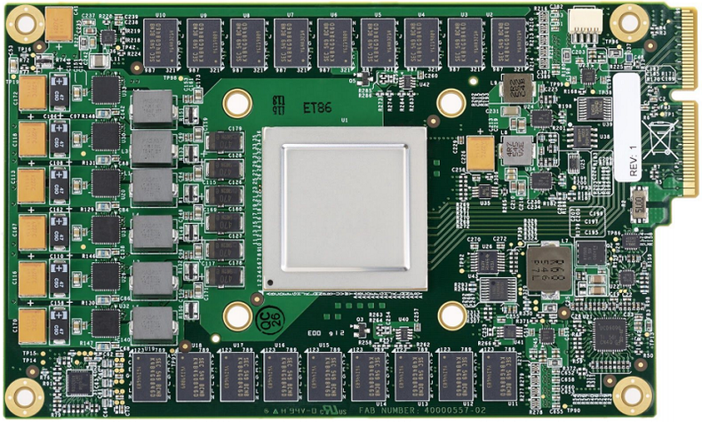
ASIC TPU takes advantage of this by enabling an 8-bit matrix multiplier, which can execute 64 K multiplication operations in parallel. With maximum performance, it provides 92 trillion operations per second. The processor also has 24 MB of internal memory, which is quite a large amount for a chip of this size. However, the memory bandwidth is rather modest - 34 Gb / s. To optimize power consumption, the TPU operates at a rather modest frequency of 700 MHz and consumes 40 watts of power. ASIC is manufactured by 28-nanometer process technology and has a TDP of 75 watts.
When it comes to computer hardware, Google focuses on power consumption, since it is a significant part of the total cost of ownership (TCO) equipment in data centers. And for large data centers, energy costs can grow too quickly in the case when the equipment is too powerful for the tasks to be performed. According to the authors of TPU analysis from Google, “when you buy equipment with thousands of units, the cost of productivity is more important than the performance itself”.
Another important aspect of TPU design is response time. Since the output is performed in response to user requests, the system should produce a result as quickly as possible. Therefore, developers preferred low latency over high throughput. For graphics processors, this ratio is reversed, so they are used in the training phase that requires a large computational power.
The validity of the development of a special chip for the "output" came to Google about six years ago, when they began to introduce "deep learning" technologies in their search engines. Since these products were used daily by millions of people, the required computing power began to look daunting. For example, it turned out that if people used voice search using a neural network for only three minutes a day, the company would have to double the number of Google data centers, provided that they use conventional equipment.
Because TPUs are specifically designed for "output", they provide much better performance and energy efficiency than Intel processors or NVIDIA graphics processors. To determine the capabilities of TPU, Google compared it with other processors of 2015, designed for "output", namely the Intel Haswell Xeon and the NVIDIA K80 graphics processor. The tests were conducted on six benchmarks for the three most commonly used types of neural networks: convolutional (CNN), recurrent (RNN), and multilayer perceptron (MLP). The corresponding configurations and test results are shown in the table below.
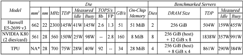
As a result, it was found that the TPU worked from 15 to 30 times faster than the K80 GPU and the Haswell processor. Energy efficiency was even more impressive, TPU outperformed competitors by 30-80 times. Google claims that if they used higher bandwidth GDDR5 memory in TPU, they could triple the chip's performance.
These results are not so surprising, given that the K80 GPU is focused on HPC and neural network training, but is not optimized for output. As for the Xeon processors, they are not optimized for "deep learning" of algorithms of any type, although in similar scenarios they are only slightly slower than the K80.
To some extent, all this is old news. The new line of NVIDIA processors in 2017 from the Pascal family surpasses the K80 by a large margin. As for the output, NVIDIA now offers the Tesla P4 and P40 GPUs, which, like TPU, support 8-bit integer operations. These NVIDIA processors may not be fast enough to outperform specialized TPUs, but the performance gap between them is likely to be significantly smaller.
In any case, TPU does not threaten NVIDIA's leadership in the field of “deep learning”. The GPU maker still dominates in this area and, obviously, is going to sell many of its “output” accelerators P4 and P40 to large data centers. NVIDIA's more common development threat for “output” is Intel, which positions its Altera FPGA for this type of work. So, Microsoft has already signed a contract for the supply of Altera FPGA, deploying the world's largest cloud of AI using Altera / Intel processors. Other AI service providers may also follow suit.
Almost certainly, Google is already working on its second-generation TPU. This chip is likely to have higher bandwidth memory, either GDDR5, or something more exotic. Google engineers will surely experiment with the logic and design of the TPU to increase the clock frequency. Moving to a smaller process, say, 14 nanometers, would make it easier to achieve these goals. Of course, it is quite possible that these TPUs have already been released and are being used in some part of the Google cloud - but this, if we learn, then only in a couple of years.
First, a little context. TPU is a specialized ASIC, developed by Google engineers to speed up the “output” processes (meaning getting the finished result - approx. Translator) of neural networks, its goal is to accelerate the productive phase of these applications for already trained networks. For example, it works every time a user initiates a voice search, requests translation of a text, or searches for a match with an image. But at the learning stage, Google uses the GPU, just like all companies that use the “deep learning” technology.
The distinction is important because “output” can be performed mostly with 8-bit integer operations, while training is usually done with 32-bit or 16-bit floating point operations. As Google indicated in its analysis of TPU , when multiplying 8-bit integers, you can use six times less energy than when multiplying 16-bit floating-point numbers, and for addition - thirteen times less.
')
ASIC TPU takes advantage of this by enabling an 8-bit matrix multiplier, which can execute 64 K multiplication operations in parallel. With maximum performance, it provides 92 trillion operations per second. The processor also has 24 MB of internal memory, which is quite a large amount for a chip of this size. However, the memory bandwidth is rather modest - 34 Gb / s. To optimize power consumption, the TPU operates at a rather modest frequency of 700 MHz and consumes 40 watts of power. ASIC is manufactured by 28-nanometer process technology and has a TDP of 75 watts.
When it comes to computer hardware, Google focuses on power consumption, since it is a significant part of the total cost of ownership (TCO) equipment in data centers. And for large data centers, energy costs can grow too quickly in the case when the equipment is too powerful for the tasks to be performed. According to the authors of TPU analysis from Google, “when you buy equipment with thousands of units, the cost of productivity is more important than the performance itself”.
Another important aspect of TPU design is response time. Since the output is performed in response to user requests, the system should produce a result as quickly as possible. Therefore, developers preferred low latency over high throughput. For graphics processors, this ratio is reversed, so they are used in the training phase that requires a large computational power.
The validity of the development of a special chip for the "output" came to Google about six years ago, when they began to introduce "deep learning" technologies in their search engines. Since these products were used daily by millions of people, the required computing power began to look daunting. For example, it turned out that if people used voice search using a neural network for only three minutes a day, the company would have to double the number of Google data centers, provided that they use conventional equipment.
Because TPUs are specifically designed for "output", they provide much better performance and energy efficiency than Intel processors or NVIDIA graphics processors. To determine the capabilities of TPU, Google compared it with other processors of 2015, designed for "output", namely the Intel Haswell Xeon and the NVIDIA K80 graphics processor. The tests were conducted on six benchmarks for the three most commonly used types of neural networks: convolutional (CNN), recurrent (RNN), and multilayer perceptron (MLP). The corresponding configurations and test results are shown in the table below.
As a result, it was found that the TPU worked from 15 to 30 times faster than the K80 GPU and the Haswell processor. Energy efficiency was even more impressive, TPU outperformed competitors by 30-80 times. Google claims that if they used higher bandwidth GDDR5 memory in TPU, they could triple the chip's performance.
These results are not so surprising, given that the K80 GPU is focused on HPC and neural network training, but is not optimized for output. As for the Xeon processors, they are not optimized for "deep learning" of algorithms of any type, although in similar scenarios they are only slightly slower than the K80.
To some extent, all this is old news. The new line of NVIDIA processors in 2017 from the Pascal family surpasses the K80 by a large margin. As for the output, NVIDIA now offers the Tesla P4 and P40 GPUs, which, like TPU, support 8-bit integer operations. These NVIDIA processors may not be fast enough to outperform specialized TPUs, but the performance gap between them is likely to be significantly smaller.
In any case, TPU does not threaten NVIDIA's leadership in the field of “deep learning”. The GPU maker still dominates in this area and, obviously, is going to sell many of its “output” accelerators P4 and P40 to large data centers. NVIDIA's more common development threat for “output” is Intel, which positions its Altera FPGA for this type of work. So, Microsoft has already signed a contract for the supply of Altera FPGA, deploying the world's largest cloud of AI using Altera / Intel processors. Other AI service providers may also follow suit.
Almost certainly, Google is already working on its second-generation TPU. This chip is likely to have higher bandwidth memory, either GDDR5, or something more exotic. Google engineers will surely experiment with the logic and design of the TPU to increase the clock frequency. Moving to a smaller process, say, 14 nanometers, would make it easier to achieve these goals. Of course, it is quite possible that these TPUs have already been released and are being used in some part of the Google cloud - but this, if we learn, then only in a couple of years.
Source: https://habr.com/ru/post/326308/
All Articles