Count to three: two
Ternary calculations
So, I continue the cycle of articles on the development of the ternary calculator. The last time we met with the most basic element: the ternary (de-) multiplexer, as well as on its base, we built a semi- and full adder. This time we will talk about memory cells.
In the last article I explained in detail why I need it: it will be a demonstration piece of hardware. Do not be lazy, check out my motivation.
So, here is a list of published articles of the cycle (will be updated):
')
- We count to three: time (ternary multiplexer and adders)
- We count to three: two (memory)
- We count to three: three (counters)
- We count to three: four (one-digit computer and a three-team command system)
I remind you that the only building block of the calculator will be the ternary multiplexer. Here is a photo of the original Trimux design by Alexander Shabarshin and my performance on surface mounting. One such board carries two ternary (de-) multiplexers:

My version of the trimmix for surface mounting was conceived for a relatively easy reproduction “on the knee”: the board, though two-sided, but contains only 12 vias. By the way, on the forum nedopc.org ran through the option for through-wiring without a single transition hole:
However, it still requires drilling holes for the output of the microcircuits, so my version is more economical :)
trimuxIO
My goal is not theorizing, but building a completely tangible piece of iron. At the moment I got some number of multiplexers that I test on dummies. Last time, all the entrances of the tested circuits were jumpers on dummies, and the outputs were a set of svetodids on the same dummy. This is rather inconvenient (especially poking the entrances), so I saw from Alexander something like this design of one input-output:
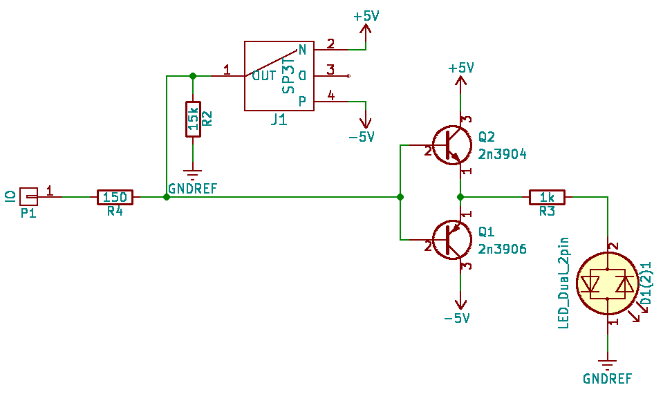
Each input-output carries one three-position switch, which by default (middle position) is slightly pulled to 0V. If the pin is used to indicate the output of the trims, the switch should be left in the middle position, and then the trimux will drag the weak pull-up to 0V. The emitter follower provides a reliable indication of even the weakest signals.
If the pin needs to be used as an input, then the switch can be connected either to + 5V or to -5V. A 150Ohm resistor protects the circuit from short circuit.
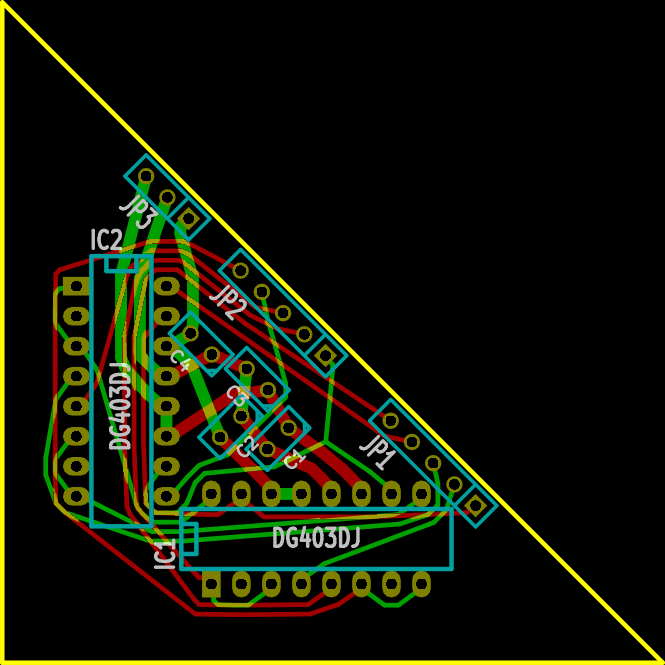
The I / O test board bears on itself 9 absolutely identical circuits:

The board is designed for easy reproduction at home: it is single-layer and does not contain any jumpers. And this is how the I / O board can be connected for testing, for example, a static memory cell:

There are three inputs: C, A, B and one output Q.
Static memory cell (ternary memorized trigger by level)
Let's connect two multiplexers (I remind you, they fit on a single trimax shawl) as follows:
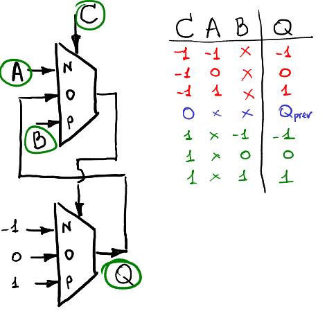
Let's agree on terminology: clocked triggers are divided into level -controlled and front -driven. Now we are talking about level control, which means that with one level of the clock signal C (-1 or 1) the trigger perceives the input signals (A or B, respectively), and with the other (0) it does not perceive and remains in the same position.
Our scheme consists of two multiplexers, the second multiplexer is simply a transparent buffer, and the first (depending on the clock signal C) outputs the second either A or B, or the output buffer itself! This means the following behavior: when C = -1, output Q closes to input A, when C = 1, output Q closes to input B, and when C = 0, output Q is kept constant and inputs A and B are simply ignored. In the text it can be messy, so watch the following video:
Dynamic memory cell: a ternary trigger with front control
In contrast to level control, with edge control, permission to switch a trigger is given only at the time of a clock drop. The rest of the time, regardless of the level of the clock signal, the trigger does not perceive the input signals and remains unchanged.
Excursion to a well-studied area
Let's take a trip to the binary (brrr) world for a moment to make it a little clearer. In the Russian-language literature, the word “trigger” is applied to all such schemes (correct me, I only found the mask). The level controlled binary trigger is called gated D-latch . Roughly speaking, it has two inputs: D (data) and E (enable). The only output Q is equal to D if E = 1, and retains its value if E = 0.
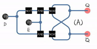
A flip-flop trigger (flip-flop) can be built from two ordinary latches (gated D-latch) and one inverter:

This scheme is called Master-slave edge-triggered D flip-flop.
Back to the ternary world or terra (almost) incognita
If we want to trigger on the front of a clock signal, we, just like in the binary world, can use two ternary latches and one equivalent of a binary inverter, as in this diagram:

Our dynamic memory cell has two inputs: C and Am; it has one Qs output. In the binary world, the inverter generates a second phase shifted signal that clocks the slave latch. In our ternary scheme, the clock signal is split into two: min (C, 0) and max (C, 0), each of which clocks its own latch. In order for the signal Am to reach the output Qs, we need two consecutive rising edges on the signal C:

Please note that immediately after switching on the circuit, before signal C sweeps from minus one to one, the output signal Qs is undefined. Initialize your variables :)
By the way, note that both the master and the slave latches have one of the inputs not used. This can be used to quickly initialize the memory, but more on that next time.
Here are the relevant video work of the memory cell with dynamic control:
Conclusion
We considered two options for memory cells. The memory cell with dynamic control is the main element of the ternary counter, which we will consider next time. Then let's talk about the ALU and the like. Of course, getting even one kilotrit of memory in this way is a very expensive (if done on the knee) lesson, but since my piece of iron will be designed for demonstration purposes and with a much smaller amount of memory, it is not so scary.
Enjoy!
Source: https://habr.com/ru/post/324650/
All Articles