Getting started in STM32CubeMX. Part 3
We continue the cycle about the basics of the work of the STM32MXCube and the programming of the STM32 microcontrollers.
→ Part 1
→ Part 2
In the last parts we mastered the basic settings of the microcontroller, work with GPIO, timer, DMA and DAC. In this part we will get acquainted with ADC and USB.
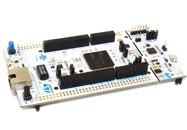
First, I want to say that from this part I will use the NUCLEO-F767ZI debugging board. This board is more accessible than the STM32F746G Discovery, uses a microcontroller in the LQFP144 package, not BGA, and the board itself is more convenient for embedding in different DIY projects. It has Ethernet and USB, as well as a JTAG debugger. The disadvantage of the board is the lack of LCD, but we do not need it yet.
Although the board has a different microcontroller, all projects from the previous parts are transferred to it almost unchanged (you only need to change pin numbers). Also note that on this board the microcontroller is clocked by a 8 MHz source. Quartz for clocking the microcontroller is provided by the scheme, but not soldered, the 8 MHz signal is removed from the JTAG debugger. If your project uses a USB interface, then it is advisable to include clocking from HSE, and not from the internal RC oscillator, since the RC oscillator does not have sufficient accuracy and frequency stability. If you try to turn on the RC oscillator if there is a USB in the project, the STM32CubeMX will issue a warning and will offer to switch to HSE (that is, to an external highly stable clock source). In order to enable an external clock source (8 MHz) on the PinOut tab, you should enable HCE in the RCC item and select BYPASS Clock Source. In practice, the USB interface still works, even from RC, but it's better not to risk it.
')
I transferred the projects from the previous parts to this board and uploaded them to the githab .
In the comments to the previous installments there were questions about the IDE. STM32CubeMX allows you to automatically create projects for various IDE: IAR (EWARM), MDK ARM v4, MDK ARM v5, Atollic TRUEStudio, SW4STM32, etc. I use Atollic TRUEStudio, which is available for download from the official site for free.
I also checked the material from the previous parts and made a number of amendments.
I want to thank Shamrel for the valuable comments on the previous part.
One of the simplest modes of USB is VCP - Virtual COM Port. Setting up work with it will require minimal effort from you.
In STM32CubeMX, find the USB_OTG_FS section on the Pinout tab and set the Mode = Device_Only:

In the USB_DEVICE section, set Class For FS IP to CDC VCP (Communication Device Class Virtual Com Port) mode:

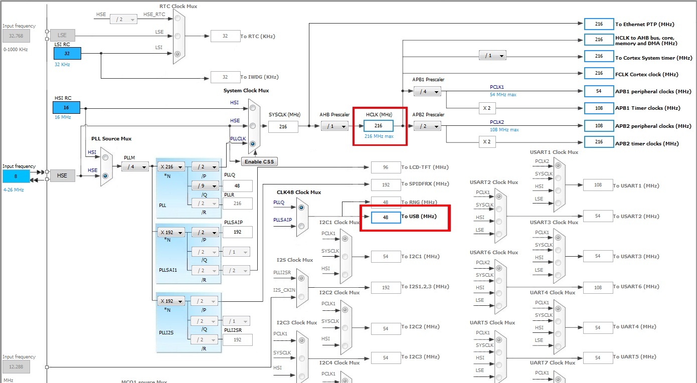
Now you need to configure the clocking configuration so that the USB frequency is 48 MHz:
Go further to the Configuration tab, and disable the VBUS Sensing parameter:

We generate the code and open the project in the IDE.
Find the file usbd_cdc_if.c and insert the following into it:
and
Here the echo mode is implemented: everything that comes to the port, we immediately send back.
We compile and flash the microcontroller. Then we connect the User USB connector of the board to the computer. The system should detect a new COM port.
For Linux: check ls / dev / tty *, the device appeared / dev / ttyACM0. Check, and here we are waiting for another surprise: denied access. You need to add yourself to the dialout group:
(where user is your username)
To work with the device in Windows, you will need to download and install the driver . To work on OS X and Linux, a special driver is not needed.
We start (for example) Putty, we configure port parameters. They must match the parameters specified in the port properties (see “Device Manager / Ports”).
We try to open the port in Putty and send something to the port:

If the port does not open, you can try to exit debug mode in the IDE and restart the board. Everything has to earn.
Addition from desinerSTM :
As we have seen, working with USB in the mode of a virtual COM port is very simple. The only drawback of this mode is the very low data transfer rate. The USB interface in Full Speed mode provides up to 12 Mbps, in High Speed mode - up to 480 Mbps, but the VCP limits the speed to a measly 128 Kbps.
You can make a high data transfer rate, but for now let's put it off until the next time.
Now let's try to run the ADC, get values from it and send it to a computer, implementing a very simple (and very slow) "oscilloscope". To make it more interesting, we will apply a sine wave formed by the DAC to the ADC. Since we have already done this in the last part, I will simply copy the code into a new project (with minor changes that do not play a big role).
First, a little about the ADC, built into the microcontroller. The STM32F767ZI microcontroller has three 12-bit ADCs, such as SAR (sequential approximation), with a capacity of up to 2 MSPS (million samples per second). This type of ADC is characterized by high conversion speed, but less accuracy than sigma-delta ADC. The reference voltage input VREF is connected to VDDA, and, through inductance, to VDD. Thus, the reference voltage in our case is 3.3V. A feature of SAR ADC is the use of a capacitor at the input to the sampling-storage circuit. At the time of sampling the signal value, the capacitor is connected to the input and charged to the size of the input signal. If the signal source has too much internal resistance, the capacitor will not have time to fully charge, and we will get a lower value. This and other aspects of using the ADC are described in [1].
The ADC of this microcontroller has many modes of operation [2], we consider only one of them. Let's try to simultaneously receive two signal values from two ADCs, strictly synchronously, and write them to the buffer via DMA.
So, we create a new project, add the ready code to it to generate a sine wave on the DAC and for the USB VCP (through it we will send data to the computer). Further (by wires) we connect the output of the DAC with the inputs of ADC1 and ADC2. In order to somehow distinguish the signals on the analog inputs, I connected ACP1 to a DAC directly, and ACP2 - through a voltage divider on a variable resistor, so that you can change the amplitude of the signal.
We will need two timers in our project. One of them will set the period of the DAC, the second - the ADC. Let's configure the analog-digital converter to work in dual channel mode with simultaneous sampling. Sampling will occur on timer TIM2. The resulting values will be buffered using DMA.
We will use the single-time DMA mode (there is also a cyclic mode, we already met him while studying the DAC). After the buffer is filled with values from the ADC, we copy its contents to another buffer (with some processing), transfer it via USB and start the process again. Also, for debugging and indication of the operation mode, we use two GPIO ports to which the LEDs are connected.
So, we have created a project in which we added a DAC and a timer TIM1. We also need to add ADC1 (input IN9), ADC2 (input IN12) and timer TIM2. We also need USB_OTG_FS.
We configure ADC1 to work in the mode of simultaneous sampling, with the launch on timer 2:

ADC2 is automatically configured:

Configure DMA:
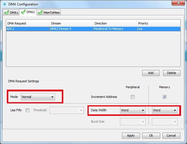
Please note that the size of the transmitted data is Word, not Half Word, because data from two ADCs, packed in a 32-bit word, are transmitted at one time. Configuring timer TIM2:

We set up USB in the same way as we did before. We generate the code.
I will not paint here the entire source code of the project, I’ll dwell only on the key points. Starting the ADC-DMA chain:
Interrupt Handler:
Why can't we directly transfer the contents of the source buffer via USB? Since the VCP speed is too low, we will not be able to transmit the entire data stream from the ADC. We capture a piece of the signal, transfer it “up”, then capture the next piece, etc. If we do not take special measures, then random fragments of the original signal will be transmitted to the port. Therefore, you need to make a software analogue of the "trigger", like a digital oscilloscope. We will send to the port not a random fragment captured by the ADC, but a piece of the signal after the occurrence of some condition. Such a condition can be the crossing of a certain level in the bottom-up direction: sample0_0 <threshold && sample0_1> = threshold, where threshold is the threshold.
That is why we make the ADC buffer twice the size of the VCP buffer, and scan it to the middle in search of such a condition. If the condition has not come, do not send anything to the port, and run the next ADC cycle.
DMA packs signals from two ADCs into one 32-bit word. We will not change this format, just add one to the high order of the first report in the buffer so that the top-level software can recognize the beginning of the “frame”:
To display the signal on the computer, I wrote a small C # program:

It is mainly assembled from components in Visual Studio and contains minimal code. Its source is also available on Github.
In the next part, we look at the Ethernet interface and a bit of the real-time operating system FreeRTOS.

Project sources for the entire series of articles can be downloaded on github . All projects are made for the Nucleo F767ZI board and use IDE Atollic TRUEStudio.
[1] AN2834 Application note. How to get the best ADC accuracy in STM32 microcontrollers
[2] AN3116 Application note. STM32's ADC modes and their applications
[3] Cookbook for SAR ADC Measurements. Freescale Semiconductor. AN4373
Thank you for your attention, please report any errors and typos in PM. To be continued.
→ Part 1
→ Part 2
In the last parts we mastered the basic settings of the microcontroller, work with GPIO, timer, DMA and DAC. In this part we will get acquainted with ADC and USB.
A small introduction to the third part
First, I want to say that from this part I will use the NUCLEO-F767ZI debugging board. This board is more accessible than the STM32F746G Discovery, uses a microcontroller in the LQFP144 package, not BGA, and the board itself is more convenient for embedding in different DIY projects. It has Ethernet and USB, as well as a JTAG debugger. The disadvantage of the board is the lack of LCD, but we do not need it yet.
Although the board has a different microcontroller, all projects from the previous parts are transferred to it almost unchanged (you only need to change pin numbers). Also note that on this board the microcontroller is clocked by a 8 MHz source. Quartz for clocking the microcontroller is provided by the scheme, but not soldered, the 8 MHz signal is removed from the JTAG debugger. If your project uses a USB interface, then it is advisable to include clocking from HSE, and not from the internal RC oscillator, since the RC oscillator does not have sufficient accuracy and frequency stability. If you try to turn on the RC oscillator if there is a USB in the project, the STM32CubeMX will issue a warning and will offer to switch to HSE (that is, to an external highly stable clock source). In order to enable an external clock source (8 MHz) on the PinOut tab, you should enable HCE in the RCC item and select BYPASS Clock Source. In practice, the USB interface still works, even from RC, but it's better not to risk it.
')
I transferred the projects from the previous parts to this board and uploaded them to the githab .
In the comments to the previous installments there were questions about the IDE. STM32CubeMX allows you to automatically create projects for various IDE: IAR (EWARM), MDK ARM v4, MDK ARM v5, Atollic TRUEStudio, SW4STM32, etc. I use Atollic TRUEStudio, which is available for download from the official site for free.
I also checked the material from the previous parts and made a number of amendments.
I want to thank Shamrel for the valuable comments on the previous part.
USB VCP
One of the simplest modes of USB is VCP - Virtual COM Port. Setting up work with it will require minimal effort from you.
In STM32CubeMX, find the USB_OTG_FS section on the Pinout tab and set the Mode = Device_Only:
In the USB_DEVICE section, set Class For FS IP to CDC VCP (Communication Device Class Virtual Com Port) mode:
Now you need to configure the clocking configuration so that the USB frequency is 48 MHz:
Go further to the Configuration tab, and disable the VBUS Sensing parameter:
We generate the code and open the project in the IDE.
Find the file usbd_cdc_if.c and insert the following into it:
static int8_t CDC_Receive_FS (uint8_t* Buf, uint32_t *Len) { /* USER CODE BEGIN 6 */ USBD_CDC_SetRxBuffer(&hUsbDeviceFS, &Buf[0]); CDC_Transmit_FS(Buf, *Len); USBD_CDC_ReceivePacket(&hUsbDeviceFS); return (USBD_OK); /* USER CODE END 6 */ } and
uint8_t CDC_Transmit_FS(uint8_t* Buf, uint16_t Len) { uint8_t result = USBD_OK; /* USER CODE BEGIN 7 */ USBD_CDC_SetTxBuffer(&hUsbDeviceFS, Buf, Len); result = USBD_CDC_TransmitPacket(&hUsbDeviceFS); /* USER CODE END 7 */ return result; } Here the echo mode is implemented: everything that comes to the port, we immediately send back.
We compile and flash the microcontroller. Then we connect the User USB connector of the board to the computer. The system should detect a new COM port.
For Linux: check ls / dev / tty *, the device appeared / dev / ttyACM0. Check, and here we are waiting for another surprise: denied access. You need to add yourself to the dialout group:
sudo adduser user dialout (where user is your username)
To work with the device in Windows, you will need to download and install the driver . To work on OS X and Linux, a special driver is not needed.
We start (for example) Putty, we configure port parameters. They must match the parameters specified in the port properties (see “Device Manager / Ports”).
We try to open the port in Putty and send something to the port:
If the port does not open, you can try to exit debug mode in the IDE and restart the board. Everything has to earn.
Addition from desinerSTM :
how to deal with error code 10 virtual port?
Helps usbd_cdc.h file instead of 512 to put 256 in the line:
#define CDC_DATA_HS_MAX_PACKET_SIZE (512 was) 256 / * Endpoint IN & OUT Packet size * /
As we have seen, working with USB in the mode of a virtual COM port is very simple. The only drawback of this mode is the very low data transfer rate. The USB interface in Full Speed mode provides up to 12 Mbps, in High Speed mode - up to 480 Mbps, but the VCP limits the speed to a measly 128 Kbps.
You can make a high data transfer rate, but for now let's put it off until the next time.
ADC
Now let's try to run the ADC, get values from it and send it to a computer, implementing a very simple (and very slow) "oscilloscope". To make it more interesting, we will apply a sine wave formed by the DAC to the ADC. Since we have already done this in the last part, I will simply copy the code into a new project (with minor changes that do not play a big role).
First, a little about the ADC, built into the microcontroller. The STM32F767ZI microcontroller has three 12-bit ADCs, such as SAR (sequential approximation), with a capacity of up to 2 MSPS (million samples per second). This type of ADC is characterized by high conversion speed, but less accuracy than sigma-delta ADC. The reference voltage input VREF is connected to VDDA, and, through inductance, to VDD. Thus, the reference voltage in our case is 3.3V. A feature of SAR ADC is the use of a capacitor at the input to the sampling-storage circuit. At the time of sampling the signal value, the capacitor is connected to the input and charged to the size of the input signal. If the signal source has too much internal resistance, the capacitor will not have time to fully charge, and we will get a lower value. This and other aspects of using the ADC are described in [1].
The ADC of this microcontroller has many modes of operation [2], we consider only one of them. Let's try to simultaneously receive two signal values from two ADCs, strictly synchronously, and write them to the buffer via DMA.
So, we create a new project, add the ready code to it to generate a sine wave on the DAC and for the USB VCP (through it we will send data to the computer). Further (by wires) we connect the output of the DAC with the inputs of ADC1 and ADC2. In order to somehow distinguish the signals on the analog inputs, I connected ACP1 to a DAC directly, and ACP2 - through a voltage divider on a variable resistor, so that you can change the amplitude of the signal.
Caution, analog circuitry!
If you feed a signal from an external source to the ADC input, remember that the signal at any input of the microcontroller should be limited to 0 - Vcc, which in most practical cases makes it necessary to shift and amplify (or weaken) the signal.
It should also be noted that the STM32 microcontrollers use sequential approximation (SAR) ADCs, which consume a fairly large current from the signal source at the time of measurement, and require a low impedance signal source.
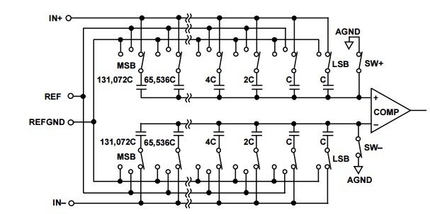
Fig. 1. SAR ADC sample-storage scheme (not from STM32, but completely analogous)
At the moments of signal sampling, capacitors (Fig. 1) are connected to the input of the ADC and must be charged to a full signal level in a very short time, while consuming a significant current. If the signal source has a high resistance, they will not have time to charge, and the ADC readings will be incorrect. In practice, this means that we must in most cases use an external buffer amplifier. Since today we will focus on the software aspects of the task, we can do without an amplifier, but remember that without an amplifier, the ADC readings will be significantly distorted, and in real projects it is needed.

Fig. 2. The sampling-storage scheme causes dips in the signal level at the ADC input.
Unfortunately, in the STM32 documentation these issues are poorly addressed, but I can recommend the manual [3].
If readers will be interested, I can consider the basics of analog node mapping circuitry in the next article.
It should also be noted that the STM32 microcontrollers use sequential approximation (SAR) ADCs, which consume a fairly large current from the signal source at the time of measurement, and require a low impedance signal source.
Fig. 1. SAR ADC sample-storage scheme (not from STM32, but completely analogous)
At the moments of signal sampling, capacitors (Fig. 1) are connected to the input of the ADC and must be charged to a full signal level in a very short time, while consuming a significant current. If the signal source has a high resistance, they will not have time to charge, and the ADC readings will be incorrect. In practice, this means that we must in most cases use an external buffer amplifier. Since today we will focus on the software aspects of the task, we can do without an amplifier, but remember that without an amplifier, the ADC readings will be significantly distorted, and in real projects it is needed.
Fig. 2. The sampling-storage scheme causes dips in the signal level at the ADC input.
Unfortunately, in the STM32 documentation these issues are poorly addressed, but I can recommend the manual [3].
If readers will be interested, I can consider the basics of analog node mapping circuitry in the next article.
We will need two timers in our project. One of them will set the period of the DAC, the second - the ADC. Let's configure the analog-digital converter to work in dual channel mode with simultaneous sampling. Sampling will occur on timer TIM2. The resulting values will be buffered using DMA.
We will use the single-time DMA mode (there is also a cyclic mode, we already met him while studying the DAC). After the buffer is filled with values from the ADC, we copy its contents to another buffer (with some processing), transfer it via USB and start the process again. Also, for debugging and indication of the operation mode, we use two GPIO ports to which the LEDs are connected.
So, we have created a project in which we added a DAC and a timer TIM1. We also need to add ADC1 (input IN9), ADC2 (input IN12) and timer TIM2. We also need USB_OTG_FS.
We configure ADC1 to work in the mode of simultaneous sampling, with the launch on timer 2:
ADC2 is automatically configured:
Configure DMA:
Please note that the size of the transmitted data is Word, not Half Word, because data from two ADCs, packed in a 32-bit word, are transmitted at one time. Configuring timer TIM2:
We set up USB in the same way as we did before. We generate the code.
I will not paint here the entire source code of the project, I’ll dwell only on the key points. Starting the ADC-DMA chain:
//start adc HAL_ADC_Start(&hadc2); HAL_ADCEx_MultiModeStart_DMA(&hadc1, (uint32_t *)adc_buf, ADC_BUF_SIZE); HAL_TIM_Base_Start_IT(&htim2); Interrupt Handler:
void HAL_ADC_ConvCpltCallback(ADC_HandleTypeDef* hadc) { HAL_TIM_Base_Stop(&htim2); HAL_ADC_Stop(&hadc2); HAL_ADCEx_MultiModeStop_DMA(&hadc1); const int threshold = (1 << 11); //find a trigger condition if(state == STARTED) { HAL_GPIO_WritePin(GPIOB, GPIO_PIN_7, 1); for(int i = 0; i < (ADC_BUF_SIZE - VCP_BUF_SIZE); i++) { uint32_t sample0_0 = adc_buf[i] & 0x00000FFF; uint32_t sample0_1 = adc_buf[i + 1] & 0x00000FFF; if(sample0_0 < threshold && sample0_1 >= threshold) //the trigger condition { memcpy(vcp_buf, adc_buf + i + 1, VCP_BUF_SIZE * sizeof(uint32_t)); vcp_buf[0] |= 0x80000000; //mark the first sample in the frame CDC_Transmit_FS((uint8_t*)vcp_buf, VCP_BUF_SIZE * sizeof(uint32_t)); } } HAL_GPIO_WritePin(GPIOB, GPIO_PIN_7, 0); } //restart adc HAL_ADC_Start(&hadc2); HAL_ADCEx_MultiModeStart_DMA(&hadc1, (uint32_t*)adc_buf, ADC_BUF_SIZE); HAL_TIM_Base_Start_IT(&htim2); //led flashing static int cnt = 0; if((cnt++) % 128 == 0) { HAL_GPIO_TogglePin(GPIOB, GPIO_PIN_14); //Toggle the state of pin } } Why can't we directly transfer the contents of the source buffer via USB? Since the VCP speed is too low, we will not be able to transmit the entire data stream from the ADC. We capture a piece of the signal, transfer it “up”, then capture the next piece, etc. If we do not take special measures, then random fragments of the original signal will be transmitted to the port. Therefore, you need to make a software analogue of the "trigger", like a digital oscilloscope. We will send to the port not a random fragment captured by the ADC, but a piece of the signal after the occurrence of some condition. Such a condition can be the crossing of a certain level in the bottom-up direction: sample0_0 <threshold && sample0_1> = threshold, where threshold is the threshold.
That is why we make the ADC buffer twice the size of the VCP buffer, and scan it to the middle in search of such a condition. If the condition has not come, do not send anything to the port, and run the next ADC cycle.
DMA packs signals from two ADCs into one 32-bit word. We will not change this format, just add one to the high order of the first report in the buffer so that the top-level software can recognize the beginning of the “frame”:
vcp_buf[0] |= 0x80000000; To display the signal on the computer, I wrote a small C # program:
It is mainly assembled from components in Visual Studio and contains minimal code. Its source is also available on Github.
What's next
In the next part, we look at the Ethernet interface and a bit of the real-time operating system FreeRTOS.
Links
Project sources for the entire series of articles can be downloaded on github . All projects are made for the Nucleo F767ZI board and use IDE Atollic TRUEStudio.
[1] AN2834 Application note. How to get the best ADC accuracy in STM32 microcontrollers
[2] AN3116 Application note. STM32's ADC modes and their applications
[3] Cookbook for SAR ADC Measurements. Freescale Semiconductor. AN4373
Thank you for your attention, please report any errors and typos in PM. To be continued.
Source: https://habr.com/ru/post/323674/
All Articles