Women's Day Gift by FPGA
Hello! On the eve of March 8, I decided to make my lover a small gift using the tools that I most often have to use at work. Having a little free time, I thought, why not write a small article on the topic about it. This is a great opportunity to congratulate all the ladies and, in particular, the small female composition of the community habrahabr. The article is written " just for fun " and has no scientific contribution, does not carry much meaning, but may be useful for novice developers in the field of FPGAs. I will tell you what tools are used to get the final result and what came of it. In the article you will see the flickering hearts and running text on the 8x8 LED matrix, which is controlled by a small old FPGA. At the end of the article you will find a video demonstration of the joint operation of the FPGA and a matrix of LEDs.
The project is implemented on a debug board with FPGA Spartan3E. It contains the simplest strapping of various interfaces (VGA, PS / 2), it has LEDs and an LED display, as well as flip-flops, buttons and various other outputs for connecting something third-party. The fee is very cheap, ordered from ebay at one of the Chinese stores. Price - $ 135.00 including shipping (~ 4000r at old prices).
The official website of the manufacturer is currently dead , which is not surprising.
The main features of the board:
')
Crystal Spartan3E XC3S500E FPGA crystal resources are listed in the table:
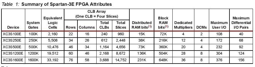
For simple projects and initial acquaintance with the FPGA design this is more than enough.
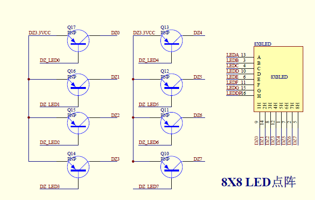
A matrix of LED8x8 LEDs is connected to the FPGA. Obviously, each LED does not connect directly, because it will require the use of 64 FPGA pins, which is very expensive and unwise! Below is a diagram of the Chinese datasheet on the debug board. It can be seen that the LEDs are connected in columns and rows of 8 pieces, and the connection is not directly, but through PNP transistors. The emitter of the transistor is connected to the supply voltage, the base to the FPGA contacts, and the collector to the matrix of LEDs. In total, 16 contacts are connected to the FPGA. The control logic of the LED matrix is negative , that is, the LEDs are lit with a low logic level (log. 0).
This means that if you set the desired logical level on a particular row and column, then a certain LED will light up.
Examples:
A) if the vector LEDY = “11111110”, and the vector LEDX = “11111110”, the single LED in the lower right corner will light up.
11111111
11111111
11111111
11111111
11111111
11111111
11111111
11111110
B) if the vector LEDY = "11111110", and the vector LEDX = "00000000", then the entire bottom line will light up.
11111111
11111111
11111111
11111111
11111111
11111111
11111111
00000000
C ) if the vector LEDY = "00000000", and the vector LEDX = "11111110", then the entire right column will light up.
11111110
11111110
11111110
11111110
11111110
11111110
11111110
11111110
D) if the vector LEDY = "00000000", and the vector LEDX = "00000000", then the whole matrix of LEDs will light up.
In this regard, there is a certain difficulty . How to light a matrix of LEDs in such a way that a certain character in the form of a letter or number is displayed on it? In fact, it is not difficult.
The process of displaying characters on a matrix of LEDs is quite simple. First, it is necessary to organize a counter of a certain digit capacity and use its three most significant digits to switch the LEDY vector. Why three digits? Switching 8-bit vector can be described using a finite state machine using 3 control bits. In VHDL, this is done like this:
Counter
The first reset (rst) is global. The second reset (rst_reg) is software and is controlled by a trigger.
State machine for LEDY
Changing the state of the counter includes one bit in the LEDY column of LEDs. Thus, the “ running zero ” scheme is organized.
Next, we need two more state machines with exactly the same logic for organizing the vector of lines LEDX . In principle, one can do without one, but it is clearer to do it in a manner similar to the column vector.
Intermediate spacecraft
KA for vector LEDX
As a result of these actions, the vector LEDX is formed. It is this vector that draws the symbols on the LED matrix, and the LEDY vector is responsible for the timely shutdown of unnecessary LEDs. In this example, the cross or the “X” symbol should light up on the LED matrix, which can be visually observed if you look closely at the last state machine. Thus, the column vector becomes auxiliary, and the row vector draws characters and with its help you can “write” anything on the LED matrix.
The project made two files of the same type of generation of symbols on a matrix of LEDs. In the first block, the heart is displayed, and in the second, the text “MARCH 8!” Is displayed using the ROM-memory design. Symbols of the text are in memory and they must be properly addressed. Since the process of displaying is fast enough, it is necessary to adjust the frequency of the display so that the characters can be read. To do this, you need to create an additional counter for 27 bits, which will divide the 50 MHz input frequency by 2 ^ 27 and allow our eye to observe the change of characters on the matrix of LEDs.
Character codes are stored in memory as a two-dimensional array. 8-bit numbers vary depending on the logic of the finite state machine (for outputting the character to the LEDs), and also depending on the address (in order to change the character on the matrix of LEDs):
Agree that if you just light a symbol on the matrix, is it a bit boring? In the project it is necessary to add special effects in the form of blinking and running lights. Make it very easy. This will require the well-known PWM algorithm (pulse width modulation). With its help, you can control the power that is supplied to the load (that is, regulate the current). This is done by varying the pulse duty cycle at a constant signal frequency.
I will not tell you how to make PWM on the FPGA, many articles have been written about it. The basic principle is that a change in the duration of the pulses of zeros and ones is organized on several controlled meters. In my project, you can control both the PWM itself (by changing the counter speed by increasing the count), and changing the data output rate to the LED matrix, changing the counter width for the LEDY column vector (by selecting the required bit fields). Taken together, this allows for various effects of twinkling, fading and running lights, which can be seen in the final video.
The FPGA project consists of several parts: these are the source code files in the VHDL language, which describe the algorithm of the microcircuit operation, and the UCF restriction file, which defines the connection of the FPGA contacts, their standard, output current, speed, restrictions on clock frequencies in the project, etc.
Pinout contacts in UCF
Top-level vhdl file
Port Description:
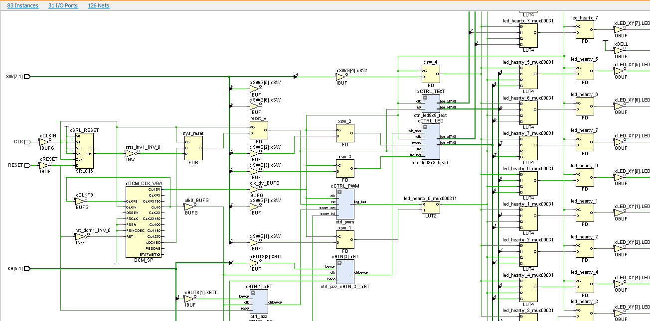
The schematic view of the project after the synthesis process is presented in the figure below. It contains input and output buffers, a DCM node, three knockout bounce contacts for the buttons and three functional nodes: PWM control, a generator of LEDs on the LED8x8 LED array, and a heart output on the matrix.
After synthesis, placement and tracing the project in the FPGA looks like this:

As you can see, the FPGA is generally empty. For resources used, the results are also shown in the figure above.
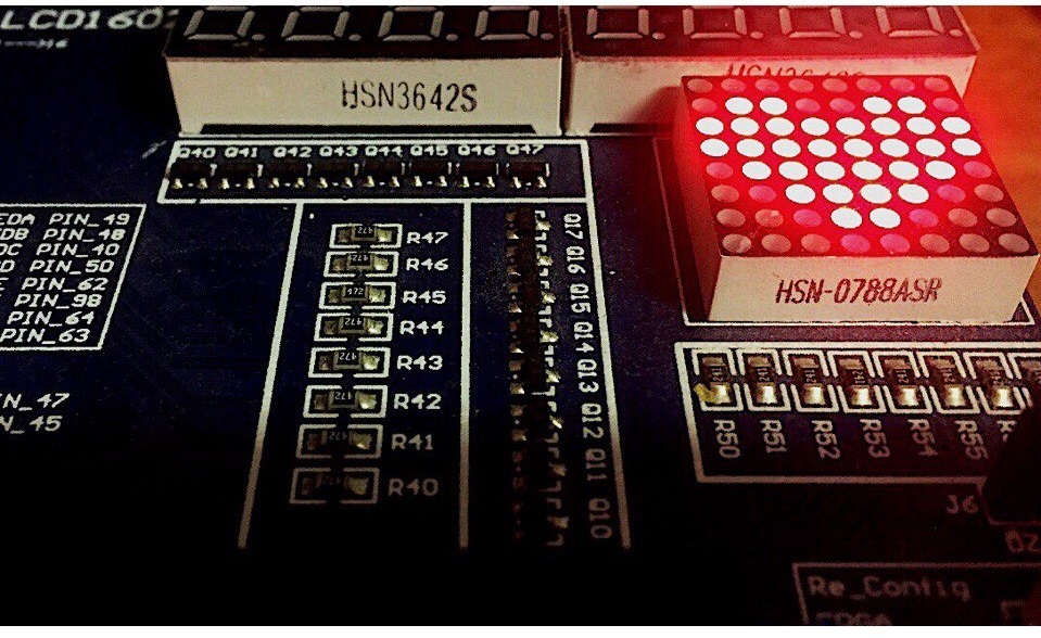
So, after the correct firmware is loaded into the FPGA and the necessary buttons are pressed, and the switches are in the correct position, the LED matrix should “come to life” and show the following features:
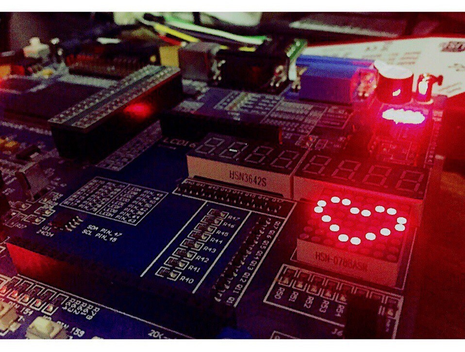
Picture: heart
Video: Shimmering and running heart
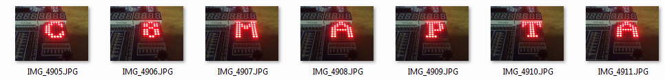
Video: Text "8 MARCH!":
The project was created in VHDL language in Xilinx ISE CAD. Work: 1 evening (project creation) + 2 pm (writing article). The source code is laid out on github , if someone is interested in doing something like this.
Once again I want to congratulate all women on the upcoming holiday. I wish you all happiness, warmth and love! In particular, I say hello to my beloved wife.
Thanks for attention!
Tool
The project is implemented on a debug board with FPGA Spartan3E. It contains the simplest strapping of various interfaces (VGA, PS / 2), it has LEDs and an LED display, as well as flip-flops, buttons and various other outputs for connecting something third-party. The fee is very cheap, ordered from ebay at one of the Chinese stores. Price - $ 135.00 including shipping (~ 4000r at old prices).
The official website of the manufacturer is currently dead , which is not surprising.
The main features of the board:
')
- FPGA Spartan3E ( XC3S500E-4PQ208C ) - 500K logic gates,
- Clock source CLK = 50 MHz,
- 64M SDRAM external memory,
- SPI Flash (M25P80) for storing FPGA firmware,
- LED matrix LED 8x8, LED line 8 pcs.,
- 8 trigger switches and 5 buttons,
- Connectors for two LED displays,
- VGA connector for connecting a monitor,
- PS / 2 connectors, etc.
Crystal Spartan3E XC3S500E FPGA crystal resources are listed in the table:
For simple projects and initial acquaintance with the FPGA design this is more than enough.
LED matrix
A matrix of LED8x8 LEDs is connected to the FPGA. Obviously, each LED does not connect directly, because it will require the use of 64 FPGA pins, which is very expensive and unwise! Below is a diagram of the Chinese datasheet on the debug board. It can be seen that the LEDs are connected in columns and rows of 8 pieces, and the connection is not directly, but through PNP transistors. The emitter of the transistor is connected to the supply voltage, the base to the FPGA contacts, and the collector to the matrix of LEDs. In total, 16 contacts are connected to the FPGA. The control logic of the LED matrix is negative , that is, the LEDs are lit with a low logic level (log. 0).
This means that if you set the desired logical level on a particular row and column, then a certain LED will light up.
Examples:
A) if the vector LEDY = “11111110”, and the vector LEDX = “11111110”, the single LED in the lower right corner will light up.
11111111
11111111
11111111
11111111
11111111
11111111
11111111
11111110
B) if the vector LEDY = "11111110", and the vector LEDX = "00000000", then the entire bottom line will light up.
11111111
11111111
11111111
11111111
11111111
11111111
11111111
00000000
C ) if the vector LEDY = "00000000", and the vector LEDX = "11111110", then the entire right column will light up.
11111110
11111110
11111110
11111110
11111110
11111110
11111110
11111110
D) if the vector LEDY = "00000000", and the vector LEDX = "00000000", then the whole matrix of LEDs will light up.
In this regard, there is a certain difficulty . How to light a matrix of LEDs in such a way that a certain character in the form of a letter or number is displayed on it? In fact, it is not difficult.
Display characters on LEDs
The process of displaying characters on a matrix of LEDs is quite simple. First, it is necessary to organize a counter of a certain digit capacity and use its three most significant digits to switch the LEDY vector. Why three digits? Switching 8-bit vector can be described using a finite state machine using 3 control bits. In VHDL, this is done like this:
Counter
pr_cnt: process(clk, rst) is begin if (rst = '0') then cnt_led <= (others => '0'); elsif rising_edge(clk) then if (rst_reg = '0') then cnt_led <= (others => '0'); else cnt_led <= cnt_led + '1'; end if; end if; end process; The first reset (rst) is global. The second reset (rst_reg) is software and is controlled by a trigger.
State machine for LEDY
pr_3x8: process(cnt_cmd) is begin case cnt_cmd is when "000" => en_xhdl <= "11111110"; when "001" => en_xhdl <= "11111101"; when "010" => en_xhdl <= "11111011"; when "011" => en_xhdl <= "11110111"; when "100" => en_xhdl <= "11101111"; when "101" => en_xhdl <= "11011111"; when "110" => en_xhdl <= "10111111"; when others => en_xhdl <= "01111111"; end case; end process; Changing the state of the counter includes one bit in the LEDY column of LEDs. Thus, the “ running zero ” scheme is organized.
Next, we need two more state machines with exactly the same logic for organizing the vector of lines LEDX . In principle, one can do without one, but it is clearer to do it in a manner similar to the column vector.
Intermediate spacecraft
pr_8x4: process(en_xhdl) is begin case en_xhdl is when "11111110" => led_cmd <= "000"; when "11111101" => led_cmd <= "001"; when "11111011" => led_cmd <= "010"; when "11110111" => led_cmd <= "011"; when "11101111" => led_cmd <= "100"; when "11011111" => led_cmd <= "101"; when "10111111" => led_cmd <= "110"; when others => led_cmd <= "111"; end case; end process; KA for vector LEDX
pr_ledx: process(led_cmd) is begin case led_cmd is when "000" => ledx <= "01111110"; when "001" => ledx <= "10111101"; when "010" => ledx <= "11011011"; when "011" => ledx <= "11100111"; when "100" => ledx <= "11100111"; when "101" => ledx <= "11011011"; when "110" => ledx <= "10111101"; when others =>ledx <= "01111110"; end case; end process; As a result of these actions, the vector LEDX is formed. It is this vector that draws the symbols on the LED matrix, and the LEDY vector is responsible for the timely shutdown of unnecessary LEDs. In this example, the cross or the “X” symbol should light up on the LED matrix, which can be visually observed if you look closely at the last state machine. Thus, the column vector becomes auxiliary, and the row vector draws characters and with its help you can “write” anything on the LED matrix.
The project made two files of the same type of generation of symbols on a matrix of LEDs. In the first block, the heart is displayed, and in the second, the text “MARCH 8!” Is displayed using the ROM-memory design. Symbols of the text are in memory and they must be properly addressed. Since the process of displaying is fast enough, it is necessary to adjust the frequency of the display so that the characters can be read. To do this, you need to create an additional counter for 27 bits, which will divide the 50 MHz input frequency by 2 ^ 27 and allow our eye to observe the change of characters on the matrix of LEDs.
Character codes are stored in memory as a two-dimensional array. 8-bit numbers vary depending on the logic of the finite state machine (for outputting the character to the LEDs), and also depending on the address (in order to change the character on the matrix of LEDs):
type rom_type is array (7 downto 0) of std_logic_vector(7 downto 0); type rom_8x8 is array (0 to 7) of rom_type; constant ROM_TEXT: rom_8x8:=( ( "11000011", "10011001", "00111101", "00111111", "00111111", "00111101", "10011001", "11000011") ... /cut -- 2D-: pr_8x8: process(clk, rst) is begin if (rst = '0') then data_led <= (others => '0'); elsif rising_edge(clk) then data_led <= ROM_TEXT(CONV_INTEGER(addr_txt(Na-1 downto Na-3)))(CONV_INTEGER(led_cmd)); end if; end process; Special effects
Agree that if you just light a symbol on the matrix, is it a bit boring? In the project it is necessary to add special effects in the form of blinking and running lights. Make it very easy. This will require the well-known PWM algorithm (pulse width modulation). With its help, you can control the power that is supplied to the load (that is, regulate the current). This is done by varying the pulse duty cycle at a constant signal frequency.
I will not tell you how to make PWM on the FPGA, many articles have been written about it. The basic principle is that a change in the duration of the pulses of zeros and ones is organized on several controlled meters. In my project, you can control both the PWM itself (by changing the counter speed by increasing the count), and changing the data output rate to the LED matrix, changing the counter width for the LEDY column vector (by selecting the required bit fields). Taken together, this allows for various effects of twinkling, fading and running lights, which can be seen in the final video.
FPGA Project
The FPGA project consists of several parts: these are the source code files in the VHDL language, which describe the algorithm of the microcircuit operation, and the UCF restriction file, which defines the connection of the FPGA contacts, their standard, output current, speed, restrictions on clock frequencies in the project, etc.
Pinout contacts in UCF
## BUTTONS = ## K1-K5 NET "KB[5]" LOC = P54; NET "KB[4]" LOC = P58; NET "KB[3]" LOC = P57; NET "KB[2]" LOC = P159; NET "KB[1]" LOC = P154; ## LEDS = ## LED_MATRIX NET "LED_X<7>" LOC = "P49" | IOSTANDARD = LVTTL | DRIVE = 8; NET "LED_X<6>" LOC = "P48" | IOSTANDARD = LVTTL | DRIVE = 8; NET "LED_X<5>" LOC = "P40" | IOSTANDARD = LVTTL | DRIVE = 8; NET "LED_X<4>" LOC = "P50" | IOSTANDARD = LVTTL | DRIVE = 8; NET "LED_X<3>" LOC = "P62" | IOSTANDARD = LVTTL | DRIVE = 8; NET "LED_X<2>" LOC = "P98" | IOSTANDARD = LVTTL | DRIVE = 8; NET "LED_X<1>" LOC = "P64" | IOSTANDARD = LVTTL | DRIVE = 8; NET "LED_X<0>" LOC = "P63" | IOSTANDARD = LVTTL | DRIVE = 8; NET "LED_Y<7>" LOC = "P75" | IOSTANDARD = LVTTL | DRIVE = 8; NET "LED_Y<6>" LOC = "P78" | IOSTANDARD = LVTTL | DRIVE = 8; NET "LED_Y<5>" LOC = "P76" | IOSTANDARD = LVTTL | DRIVE = 8; NET "LED_Y<4>" LOC = "P69" | IOSTANDARD = LVTTL | DRIVE = 8; NET "LED_Y<3>" LOC = "P74" | IOSTANDARD = LVTTL | DRIVE = 8; NET "LED_Y<2>" LOC = "P65" | IOSTANDARD = LVTTL | DRIVE = 8; NET "LED_Y<1>" LOC = "P68" | IOSTANDARD = LVTTL | DRIVE = 8; NET "LED_Y<0>" LOC = "P77" | IOSTANDARD = LVTTL | DRIVE = 8; NET "RESET" LOC = P148 | IOSTANDARD = LVTTL; NET "CLK" LOC = P183 | IOSTANDARD = LVCMOS33; NET "CLK_IN" TNM_NET = "CLK_TN"; TIMESPEC TS_CLK = PERIOD "CLK_TN" 20 ns HIGH 50 %; Top-level vhdl file
entity top_xc3s500e_heart is port( ---- SWITCHES ---- RESET : in std_logic; --! asycnchronous reset: SW(0) SW : in std_logic_vector(7 downto 1); --! other switches ---- CLOCK 50 MHz ---- CLK : in std_logic; --! main clock 50 MHz ---- LED DISPLAY ---- LED_X : out std_logic_vector(7 downto 0); --! LEDs Y LED_Y : out std_logic_vector(7 downto 0); --! LEDs X ---- BUTTONS ---- KB : in std_logic_vector(5 downto 1); --! Five Buttons ); end top_xc3s500e_heart; Port Description:
- RESET - global reset (switch SW [0]),
- CLK - 50 MHz clock speed,
- SW <1> is the PWM resolution,
- SW <2> - heart control mode,
- SW <3> - 8x8 matrix reset,
- SW <4> - switching blocks HEART / TEXT,
- KB <1> - PWM master counter speed control (total period),
- KB <2> - Control the speed of the secondary PWM counter (pulse duty cycle),
- KB <3> - Change control of 8x8 matrix counter (for LEDY vector).
- LED_X is the vector of rows of the LED matrix,
- LED_Y - vector of LED matrix columns,
The schematic view of the project after the synthesis process is presented in the figure below. It contains input and output buffers, a DCM node, three knockout bounce contacts for the buttons and three functional nodes: PWM control, a generator of LEDs on the LED8x8 LED array, and a heart output on the matrix.
After synthesis, placement and tracing the project in the FPGA looks like this:
As you can see, the FPGA is generally empty. For resources used, the results are also shown in the figure above.
Result
So, after the correct firmware is loaded into the FPGA and the necessary buttons are pressed, and the switches are in the correct position, the LED matrix should “come to life” and show the following features:
Picture: heart
Video: Shimmering and running heart
Video: Text "8 MARCH!":
The project was created in VHDL language in Xilinx ISE CAD. Work: 1 evening (project creation) + 2 pm (writing article). The source code is laid out on github , if someone is interested in doing something like this.
Once again I want to congratulate all women on the upcoming holiday. I wish you all happiness, warmth and love! In particular, I say hello to my beloved wife.
Thanks for attention!
Source: https://habr.com/ru/post/323260/
All Articles