Motion Detection in FPGA Video Stream
Foreword
I have long been interested in the topic of video processing, only on the debug shawls of the 7th and 9th ARMs, this worked out very slowly and this was not interesting.
Currently, it is full of powerful multi-core iron and many libraries have been created for working with video, but my choice fell on FPGAs.
This project originates 5 or 6 years ago, at a time when there was no Aliexpress and similar shops, where you can buy a digital camera module or a debug board with FPGA for ridiculous money. The first version of the project was launched using the HV7131GP camera from a mobile phone on a homemade board, a display from Siemens S65 and a debug board from Terasic DE2. Then 5 years the project was gathering dust on the shelf and on the disk.
It looked like this:
')
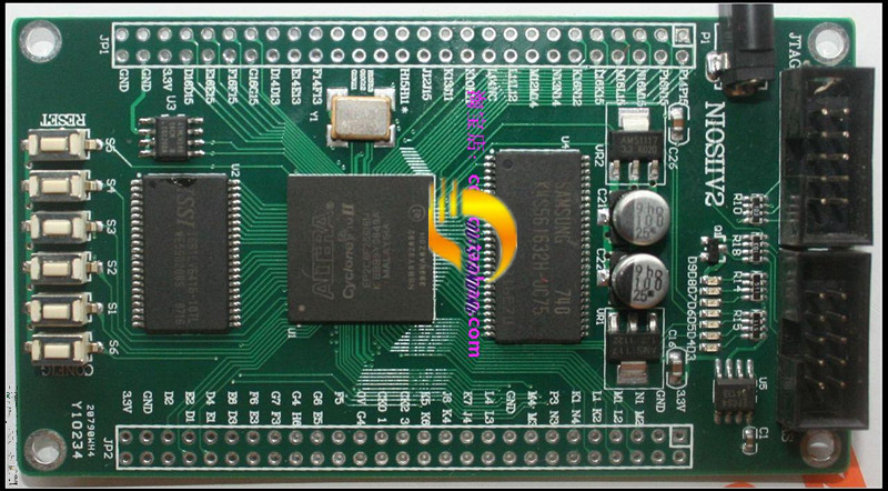
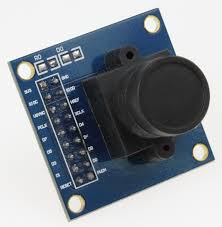
Subsequently, the Altera Cyclone II EP2C8F256 FPGA board and the OV7670 camera module were purchased specifically for this project. After purchasing the board, it turned out that there was no documentation for it and the seller did not respond to the request. Through a long network search, I found a project made on this board and borrowed assignments from it.
In this article I want to introduce the reader to methods of capturing an image from a camera, converting color space, zooming in, displaying an image through an HDMI interface and detecting the movement of objects in a video stream using FPGAs from Altera.
I want to immediately note that programming an FPGA is not my main specialization, but, more than that, a hobby in my spare time. Therefore, I may be mistaken in the conclusions made and my decisions may be far from optimal. In the pursuit of Fmax, many sections of the code were written in such a way that they may seem redundant, strange, meaningless, and suboptimal.
Tools
As the main development environment, I chose HDL Designer from Mentor Graphics. All graphic blocks and links between them are made in it. For the synthesis and tracing used environment Quartus II from Altera.
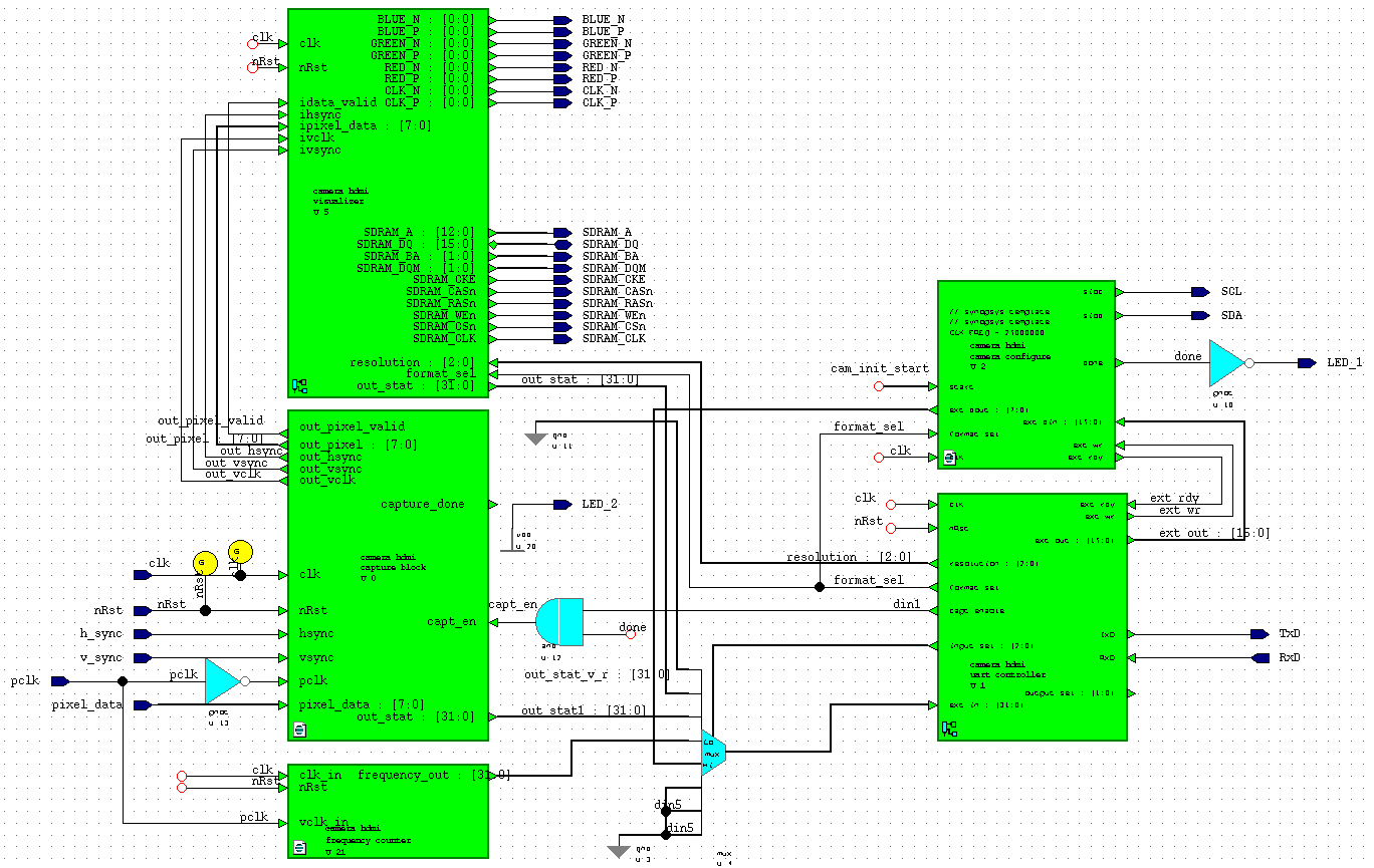
Project structure
The structural scheme of the project is shown in the figure below. It reflects only the main functional units, which will be discussed in detail below.
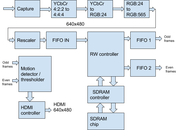
In HDL Designer, it looks like this:
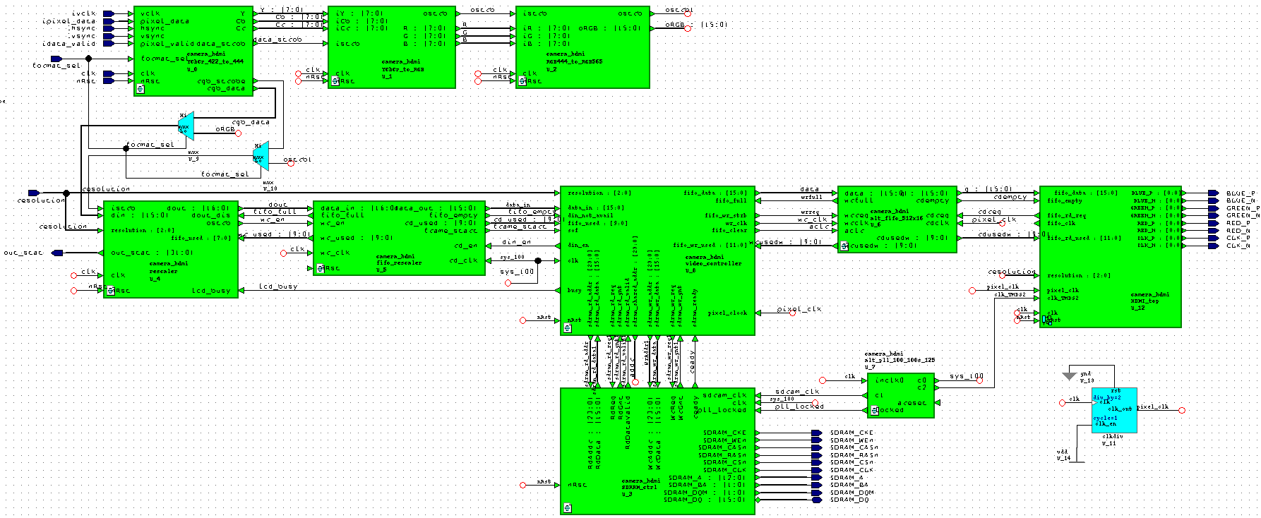
Not all project blocks are shown in the diagram. they are on a higher level.
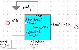
Capture module
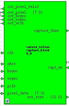 The video capture module accepts data from the pixel_data camera in the YCbCr 4: 2: 2 or RGB: 565 format and the frame and line sweep control signals hsync, vsync, translates them into the clk domain (50 MHz), generates the out_pixel_valid control signal and out_vclk and passes them to the data format conversion module. Also, this module generates out_stat statistics on the number of received data for 1 frame. Statistics can be read through the UART. The module is controlled by an external capt_en data enable signal. This signal is set by the camera setup module upon completion of the setup. Verilog code:
Capture
always @(posedge clk) begin hs_sync_1 <= hsync;hs_sync_2 <= hs_sync_1; vs_sync_1 <= vsync;vs_sync_2 <= vs_sync_1; vclk_sync_1 <= pclk;vclk_sync_2 <= vclk_sync_1; pixdata_sync_1 <= pixel_data;pixdata_sync_2 <= pixdata_sync_1; end reg vclk_old; always @(posedge clk)vclk_old <= vclk_sync_2; wire vclk_posedge = (vclk_old == 1'b0) && (vclk_sync_2 == 1'b1); reg sample_new,sample_hsync,sample_vsync; reg [7:0] sample_pixel; always @(posedge clk) begin sample_new <= vclk_posedge; if (vclk_posedge) begin sample_hsync <= hs_sync_2; sample_vsync <= vs_sync_2; sample_pixel <= pixdata_sync_2; end End reg last_vsync_sample,P2_vsync_triggered,P2_vsync_end_triggered; reg P2_sample_vsync,P2_sample_new,P2_sample_hsync; reg [7:0] P2_sample_pixel; reg P2_new_frame,capt_done,capt_enable; always @(posedge clk) begin if (capt_en == 1'b1 || P2_vsync_triggered == 1'b1) capt_enable <= 1'b1; else capt_enable <= 1'b0; end always @(posedge clk) if (!nRst) begin last_vsync_sample <= 1'b0,P2_vsync_triggered <= 1'b0; P2_vsync_end_triggered <= 1'b0,P2_new_frame <= 1'b0; capt_done <= 1'b0; end else begin if (capt_enable) begin if (sample_new) begin last_vsync_sample <= (sample_vsync/* && capt_en*/); P2_sample_pixel <= sample_pixel; P2_sample_hsync <= sample_hsync; P2_sample_vsync <= sample_vsync; end // Pipeline Step P2_sample_new <= sample_new; if (!P2_vsync_end_triggered) begin if ((last_vsync_sample == 1'b1) && (sample_vsync == 1'b0)) begin P2_vsync_triggered <= 1'b1; P2_new_frame <= 1'b1; end if (P2_vsync_triggered && sample_vsync) begin P2_vsync_end_triggered <= 1'b1; P2_vsync_triggered <= 1'b0; capt_done <= ~capt_done; end end else begin P2_vsync_end_triggered <= 1'b0; P2_vsync_triggered <= 1'b0; end if (P2_new_frame) P2_new_frame <= 1'b0; end else begin last_vsync_sample <= 1'b0;P2_vsync_triggered <= 1'b0; P2_vsync_end_triggered <= 1'b0;P2_new_frame <= 1'b0;capt_done <= 1'b0; end end Format conversion module
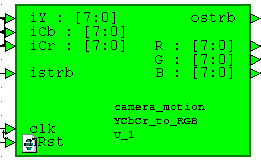
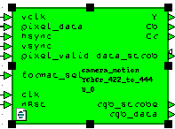 The YCbCr 4: 2: 2 format is not very convenient for further work, since the data follow in the following sequence: Y0 Cb0 Y1 Cr1 Y2 Cb2 Y3 Cr3 ... Therefore, we will convert it to the YCbCr 4: 4: 4 format. In fact, the entire conversion is reduced to issuing Y Cb Cr data per 1 clock of the data_strob signal. In Verilog it looks like this:
YCbCr 4: 2: 2 => 4: 4: 4
always @(posedge clk) if (!nRst) pix_ctr <= 2'b0; else begin if (pixel_valid) begin if (vclk) pix_ctr <= pix_ctr + 1'b1; end else pix_ctr <= 2'd0; end always @(posedge clk) case (pix_ctr) 2'd0:begin YYY <= pixel_data; CCr <= Crr; CCb <= Cbb; Ypix_clock <= 1'b1;end 2'd1:begin Cbb <= pixel_data; YY <= YYY; end 2'd2:begin YYY <= pixel_data; CCr <= Crr; CCb <= Cbb; Ypix_clock <= 1'b1;end 2'd3:begin Crr <= pixel_data; YY <= YYY; end endcase assign data_strob = Ypix_clock; assign Y = YY; assign Cb = CCb; assign Cr = CCr; Color Space Conversion Module
 In the end, we always work with data in the RGB format, so we need to get it from YCbCr. This is done according to the formula of datasheet on camera:
R = Y + 1.402 (Cr - 128)
G = Y - 0.714 (Cr - 128) - 0.344 (Cb - 128)
B = Y + 1.772 (Cb - 128)
In Verilog language looks like this:
YCbCr => RGB
parameter PRECISION = 11; parameter OUTPUT = 8; parameter INPUT = 8; parameter OUT_SIZE = PRECISION + OUTPUT; parameter BUS_MSB = OUT_SIZE + 2; always @ (posedge clk) if (!nRst) begin R_int <= 22'd0; G_int <= 22'd0; B_int <= 22'd0; end else begin if (istrb) begin //R = Y + 1.371(Cr - 128) R_int <= (Y_reg << PRECISION)+(C1*(Cr_reg-8'd128)); //G = Y - 0.698(Cr-128)-0.336(Cb-128) G_int <= (Y_reg << PRECISION)-(C2*(Cr_reg-8'd128))-(C3*(Cb_reg-8'd128)); //B = Y + 1.732(Cb-128) B_int <= (Y_reg << PRECISION)+(C4*(Cb_reg-8'd128)); end end assign R = (R_int[BUS_MSB]) ? 8'd16 : (R_int[OUT_SIZE+1:OUT_SIZE] == 2'b00) ? R_int[OUT_SIZE-1:PRECISION] : 8'd240; assign G = (G_int[BUS_MSB]) ? 8'd16 : (G_int[OUT_SIZE+1:OUT_SIZE] == 2'b00) ? G_int[OUT_SIZE-1:PRECISION] : 8'd240; assign B = (B_int[BUS_MSB]) ? 8'd16 : (B_int[OUT_SIZE+1:OUT_SIZE] == 2'b00) ? B_int[OUT_SIZE-1:PRECISION] : 8'd240; RGB format conversion module: 24 to RGB: 565
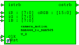 This module makes us out of a 24-bit 16-bit RGB format. It is convenient for us because Takes up less space in memory, reduces bitrate, has color reproduction acceptable for our purposes and, most importantly, fits into one word of SDRAM data, which makes work much easier. The data strobe signal is simply transmitted from the previous module.
Module code is very simple:
assign oRGB = {iR[7:3], iG[7:2], iB[7:3]}; assign ostrb = istrb; Rescaler
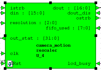 This module came to the project from the very beginning. Its goal is to convert an input stream of 640x480 pixels into a stream of 320x240, 160x120, 128x120, 80x60 and 320x480. These formats were needed to work with the LCD display from the Siemens S65, TFT display for the Arduino board and to implement image rotation in the FPGA and SDRAM block memory using the CORDIC algorithm. In other words, this is the legacy of other projects. In this project it is possible to change the screen resolution on-the-fly, and this module plays the first violin here. The module also generates statistics on the amount of data per frame for debugging. The module has been created for a long time and its code should be redeveloped, but while it works, we will not touch it.
The module code is quite capacious, and in this article I will give only its main part:
Rescaler
always @(posedge clk) if (!nRst) begin w_ctr <= 16'd0;h_ctr <= 16'd0;frame_start <= 1'b0; rsmp_w <= 8'd0;rsmp_h <= 8'd0; end else begin if (resampler_init) begin w_ctr <= 16'd0;h_ctr <= 16'd0;frame_start <= 1'b0; rsmp_w <= 8'd0;rsmp_h <= 8'd0; end else begin /* This case works ONLY if the input strobe is valid */ if (istrb) begin if (w_ctr == I_WIDTH-1'b1) begin w_ctr <= 16'd0; if (h_ctr == I_HEIGHT-1'b1) begin h_ctr <= 16'd0; frame_start <= 1'b1; end else begin h_ctr <= h_ctr + 1'b1;frame_start <= 1'b0; end if (rsmp_h == H_FACT-1'b1) begin rsmp_h <= 8'd0; end else begin rsmp_h <= rsmp_h + 1'b1; end end else begin w_ctr <= w_ctr + 1'b1; frame_start <= 1'b0; end if (rsmp_w == W_FACT-1'b1) begin rsmp_w <= 8'd0; end else begin rsmp_w <= rsmp_w + 1'b1; end end end end reg pix_valid; always @(rsmp_w or rsmp_h or wh_multiply or H_FACT) begin if (wh_multiply == 1'b1) begin pix_valid = ((rsmp_w == 8'd0) && (rsmp_h == 8'd0))?1'b1:1'b0; end else begin pix_valid = ((rsmp_w == 8'd0) && (rsmp_h != 8'd0 ))?1'b1:1'b0; end end assign pixel_valid = pix_valid; always @(posedge clk) if (!nRst) begin frame_enable <= 1'b0; end else begin if (resampler_init) begin frame_enable <= 1'b0; end else begin if (frame_start) begin if (!lcd_busy) frame_enable <= 1'b1; else frame_enable <= 1'b0; end end end reg local_frame_start = 1'b0; always @(posedge clk) if (!nRst) begin ostrb_port <= 1'b0; dout_port <= 17'd0; local_frame_start <= 1'b0; end else begin local_frame_start <= frame_start ? 1'b1: local_frame_start; if (istrb && !resampler_init && !lcd_busy) begin if (pixel_valid) begin // if our column and our row if (frame_enable && !dout_dis) begin dout_port[16:0] <= {local_frame_start, din[15:0]}; ostrb_port <= 1'b1; local_frame_start <= 1'b0; end else begin ostrb_port <= 1'b0; end end else ostrb_port <= 1'b0; end else ostrb_port <= 1'b0; end FIFO IN
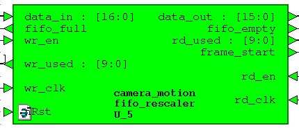 This is a two-blade FIFO dcfifo mega-function Altera 256x17. The sixteenth bit - the frame_start signal is added for convenience of indicating the start of a new frame after rescaler.
The write clock is 50 MHz, the read clock is 100 MHz, it is also a clock of the SDRAM controller.
Read-write controller
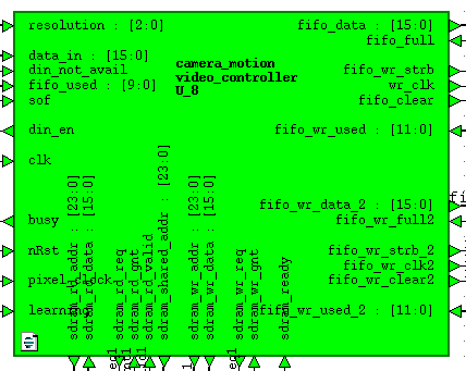 This bulky module is a single writer who takes data from the FIFO IN module and writes it to SDRAM alternately in different memory areas for even and odd frames and two readers who read data from SDRAM, each from its own memory area and write it to the weekend FIFO. Priority is given to readers, since they work on an HDMI controller with a frequency of 25 MHz (640x480), and he does not tolerate delays, there must always be data in the FIFO for processing and output to the screen. The time left from filling the output FIFO is the time of the inactive screen area plus the emptying time of the FIFO, the writer works.
When developing this module, I ran into a problem: if you use the FIFO signals full and empty, then the FIFO starts to fail and break the data. This does not happen for FIFO IN. The frequency of writing a block to it is significantly lower than the frequency of reading from it. This bug is manifested at the weekend FIFO. A write block of 100 MHz is 4 times as high as a read block of 25 MHz, which, according to my guesses, leads to the fact that the write pointer catches up with and overtakes the read pointer. I found a mention in the network of a certain Alter FIFO bug, I don’t know if it is related to my problem or not. The problem itself was solved without using the wr_full and rd_empty signals, but using the wrusedw and rdusedw signals. I made a FIFO state controller for the fifo_almost_full and fifo_almost_empty circuits. It looks like this:
// FIFO 1 wire out_fifo_almost_full = &fifo_wr_used[9:4]; wire out_fifo_almost_empty = !(|fifo_wr_used[10:8]); // FIFO 2 wire out_fifo_almost_full_2 = &fifo_wr_used_2[9:4]; wire out_fifo_almost_empty_2 = !(|fifo_wr_used_2[10:8]); Also, the module implements the change of operation modes: Background Subtraction or Frame Difference. This is achieved by the learning signal, which is connected to the clock button on the board.
I will not give all the module code, there is quite a lot of it and there is no know-how there. This module operates at a 100 MHz SDRAM frequency.
SDRAM controller
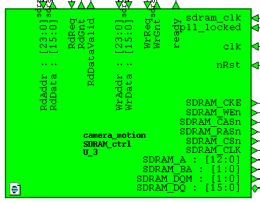 The module from the site fpga4fun.com was taken as a basis and was slightly modified for our type of SDRAM K4S561632 chip with the addition of chip initialization and additional delays to comply with the time frame:
Row active to row active delay: tRRD 15 n sec and
Row precharge time: tRP 20 n sec
The module code can be downloaded from the website at the link above. The main problem was the writing of the constraints in TimeQuest for the correct operation of our SDRAM and the selection of the phase shift of the clock by the pin SDRAM_CLK with the PLL. Otherwise, everything worked right away. Writing and reading is done by bursts, only one active bank for 4 megaslova is used, no refresh is used.
FIFO OUT
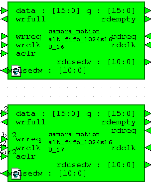 As in the case of FIFO IN, these FIFOs are two-fold mega-functions of 1024x16 dcfifo.
The write clock is 100 MHz, the read clock is 25 MHz.
Motion Detector
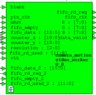 So we got to the module, which is the salt of the earth of this project. As you can see, it receives data and control signals from both output FIFOs, a slice of the HDMI 25 MHz controller pixel_clock, pixel counters counter_x, counter_y and a signal from the active display area of the blank. RGB signals come out of it, ready for display on the display.
It also implements the FIFO occupancy chains:
// FIFO 1 wire in_fifo_data_avail = |fifo_rd_used[10:4]; wire in_fifo_almost_empty = !(|fifo_rd_used[10:4]); // FIFO 2 wire in_fifo_data_avail_2 = |fifo_rd_used_2[10:4]; wire in_fifo_almost_empty_2 = !(|fifo_rd_used_2[10:4]); wire fifos_available = in_fifo_data_avail & in_fifo_data_avail_2; wire fifos_almost_empty = in_fifo_almost_empty | in_fifo_almost_empty_2; We need to control the area of the screen in which we display the picture from the camera:
wire in_frame = ((counter_x < RES_X) && (counter_y < RES_Y))?1'b1:1'b0; wire frame_start = ((counter_x == 0) && (counter_y == 0))?1'b1:1'b0; Both FIFOs are read simultaneously by the data availability flag in both of them:
// Reader FIFO 1 & 2 always @(posedge pix_clk or negedge nRst) if (!nRst) begin fifo_rd_req <= 1'b0; fifo_rd_req_2 <= 1'b0; pixel_data <= 16'h0000; worker_state <= 2'h1; end else begin case (worker_state) 2'h0: begin if (in_frame) begin if (fifos_almost_empty) begin //worker_state <= 2'h1; fifo_rd_req <= 1'b0; fifo_rd_req_2 <= 1'b0; end else begin pixel_data <= fifo_data; pixel_data_2 <= fifo_data_2; fifo_rd_req <= 1'b1; fifo_rd_req_2 <= 1'b1; end end else begin fifo_rd_req <= 1'b0; fifo_rd_req_2 <= 1'b0; end end 2'h1: begin if (blank) begin worker_state <= 2'h2; end end 2'h2: begin // start reading if more than 16 words are already in the fifo if (fifos_available && frame_start) begin fifo_rd_req <= 1'b1; fifo_rd_req_2 <= 1'b1; worker_state <= 2'h0; nd end endcase end The data read from FIFO has the format RGB: 565, for our purposes it should be converted to a black and white representation. This is done like this:
// Convert to grayscale frame 1 wire [7:0] R1 = {pixel_data[15 : 11], pixel_data[15 : 13]}; wire [7:0] G1 = {pixel_data[10 : 5], pixel_data[10 : 9]}; wire [7:0] B1 = {pixel_data[4 : 0], pixel_data[4 : 2]}; wire [7:0] GS1 = (R1 >> 2)+(R1 >> 5)+(G1 >> 1)+(G1 >> 4)+(B1 >> 4)+(B1 >> 5); // Convert to grayscale frame 2 wire [7:0] R2 = {pixel_data_2[15 : 11], pixel_data_2[15 : 13]}; wire [7:0] G2 = {pixel_data_2[10 : 5], pixel_data_2[10 : 9]}; wire [7:0] B2 = {pixel_data_2[4 : 0], pixel_data_2[4 : 2]}; wire [7:0] GS2 = (R2 >> 2)+(R2 >> 5)+(G2 >> 1)+(G2 >> 4)+(B2 >> 4)+(B2 >> 5); The GS1 and GS2 signals are our black and white presentation.
Now a little about the algorithms. There are many ways to detect motion. In this article I will consider only two of them, in my opinion, the simplest and most easily implemented in the framework of this project.
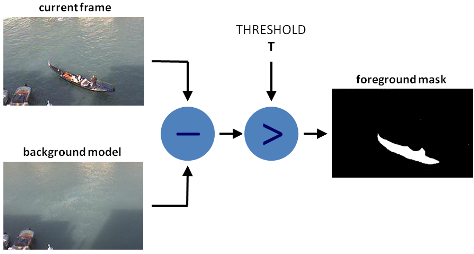
Method one. Background subtraction.
The idea is that to find a motion or an object in a video stream, subtraction is used:
P [F (t)] = P [I (t)] - P [B]
P [F (t)] - the resulting difference,
P [I (t)] - the current frame from the camera,
P [B] - reference frame or background
Reference frame or background is usually done when there is no movement. For example, if we want to detect movement in one corner of a room, then before that we must make and remember a snapshot of this angle when there is no movement there, and then subtract this pixel by pixel-by-pixel from all subsequent snapshots. Everything is very simple. However, due to noise in the image, automatic white balance in the camera and other factors, we need to apply the detector trigger threshold. This threshold applies to frame difference. If the difference is greater than the threshold, then there is movement, otherwise - no.
P [F (t)]> Threshold
There are more disadvantages to this method than advantages, however, it is used to detect movement because of its ease of implementation. Disadvantages are:
- Light dependence
- Dependence on camera shift
- Dependence on weather conditions
- Effect of auto white balance
Any change in external factors will lead to motion detection and false triggering of the detector.
Figuratively, the detector circuit looks like this:
The second way. Frame difference
This method of implementation is not much different from the previous one. All the differences lie in the fact that instead of the background, the previous frame is subtracted from the current frame and the difference is compared with the Threshold threshold.
The mathematical representation is as follows:
P [F (t)] = P [I (t)] - P [I (t - 1)]> Threshold
The advantage of this method is the relative resistance to external factors. Even with a change in camera position or illumination, this will not cause long-term false positives, but only a short-term one within two consecutive frames.
Disadvantages are:
- Frame rate dependence
- Inability to detect immovable objects
- Weak detection of objects with low speed
Due to the above disadvantages, this method has not found widespread use in its pure form.
Implementation in the Verilog language.
In our case, no matter what frame from which we subtract, the absolute difference between them is important to us.
reg [7:0] difference = 0; wire [7:0] max_val = (GS1 > GS2) ? GS1 : GS2; wire [7:0] min_val = (GS1 < GS2) ? GS1 : GS2; always @(posedge pix_clk) begin if (in_frame) begin difference <= max_val - min_val; end else difference <= 8'h00; end wire [15:0] out_val = in_frame ? (difference > `BS_THRESHOLD) ? 16'hF1_00 : pixel_data_2 : in_frame2 ? pixel_data_diff : 16'h00_00; As can be seen from the code, we replace the pixel with red (16'hF1_00), if the difference is greater than the BS_THRESHOLD threshold.
To display on the screen, we need to convert data from the RGB format: 565 to the RGB format: 24
// VGA 24 bit assign R = {out_val[15 : 11], out_val[15 : 13]}; assign G = {out_val[10 : 5], out_val[10 : 9]}; assign B = {out_val[4 : 0], out_val[4 : 2]}; HDMI controller
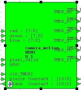
Part of this module was taken from the same site fpga4fun.com and converted according to an article from the site marsohod.org . Instead of using diff. LVDS pairs I used DDIO megafunction. For what it is done, you can read by reading the article on the link above.
Clocks
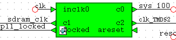
A system clock frequency of 50 MHz is taken from the generator on the board. Shreds are made from it for the SDRAM controller and the SDRAM chip. These clocks have the same frequency of 100 MHz, but are shifted in phase by 90 degrees. For this, the mega-function PLL is used
The 125 MHz clock (clk_TMDS2) is used for DDIO, after which it turns into 250 MHz. Such is the trick.
The video data pixel_clock is equal to 25 MHz, it is done by dividing by 2 system clock 50 MHz.
Camera setup OV7670
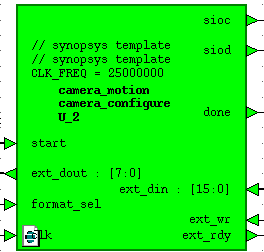 A third-party SCCB interface module is used to configure the camera. It is slightly modified for the needs of the project and is capable of recording camera register values on-the-fly upon a command from the UART interface.
UART
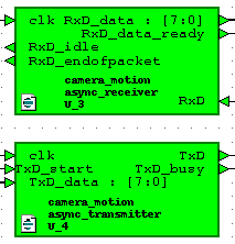 The module consists of a receiver and transmitter UART and module io_controller
The code of the receiver and transmitter modules was taken from the Internet. The modules operate at 115200 baud with 8N1 settings.
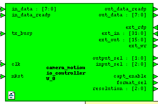
This module (io_controller) is the link between the UART transceiver and external modules of the project. It provides statistics output to the UART, receiving and processing commands. With it, you can change the display resolution, change the output format of the camera (YCbCr or RGB), record any of its registers and output any requested statistics.
Video demonstration of the result
Video quality
I apologize for the quality of the video, this is my phone.
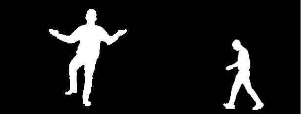
Video 1. Frame Difference
The left side of the screen displays the image from the camera in 320x240 format, and on the right is the threshold frame difference. The left image is tinted red in places where we detected movement.
The video shows that when the object is stopped, the movement is not detected, and when the speed of the object decreases, it is detected much worse.
Video 2. Background Subtraction
You can see that as the object approaches the camera, the white balance changes and we get a false trigger of the detector. Such phenomena can be filtered or compensated. One of the compensation methods is the training with the averaging of the reference image (Approximate Median Filter).
findings
This development can and should be improved by complicating the detection algorithms. It would also be nice to implement tracking of moving objects by drawing a rectangular frame around the object.
The video has horizontal rectangles. This phenomenon is associated with a read bug from the SDRAM controller, which I have not yet been able to completely overcome.
Materials on the topic
→ Article about motion detection on OpenCV
→ Yet another detector on OpenCV
→ Background subtraction
→ Methods to improve detection
UPD
As promised, I publish the project. Available on Yandex disk. This is a copy of the project made in Quartus, while I’m not going to upload it to HDL Designer, it’s unlikely that it will run for anyone even if I post it.
reference to the project
Source: https://habr.com/ru/post/323258/
All Articles