Implementation of FFT node with floating point on the FPGA
Hello! This article will discuss the implementation of the fast Fourier transform in floating point format on the FPGA. The main features of kernel development from the very first stage to the finished configurable IP core will be shown. In particular, a comparison will be made with ready-made Xilinx cores, showing the advantages and disadvantages of various implementation options. The article will tell about the main feature of the core FFT and OBPF - about the absence of the need to translate the data into natural order after the FFT and OBPF for their joint connective. In this article I will try to reflect all the subtleties of the project called FP23FFTK, I will give real examples of using the finished core. The project is written in VHDL and sharpened under the Xilinx FPGA of the last families.
In digital signal processing, without any doubt, the main analysis tool is the Fast Fourier Transform (FFT). The algorithm is used in almost all areas of science and technology. The simplest physical example of the Fourier transform is the human perception of sound. Whenever we hear a sound, the auricle automatically performs a complex calculation, which a person is able to do only after several years of studying math. The essence of the phenomenon lies in the fact that the auditory organ represents sound in the form of a spectrum of consecutive loudness values for tones of different heights, and the brain transforms the received information into perceived sound.
In matters of radio engineering, FFT algorithms are used in convolutions and in the design of digital correlators, used in image processing, as well as in audio and video equipment (equalizers, spectrum analyzers, vocoders). In addition, FFT methods underlie all sorts of data encryption and compression algorithms (jpeg, mpeg4, mp3), as well as when working with long numbers. FFT is used in sonar systems to detect surface ships and submarines, and in radar systems to obtain information about speed, flight direction and distance to targets.
')
Various FFT modules are available in almost any application package for research, such as Maple, MATLAB, GNU Octave, MathCAD, Mathematica. The specialist must understand the Fourier transform process and be able to correctly apply it to solve the set tasks, where necessary.
The first software implementation of the FFT algorithm was carried out in the early 60s of the 20th century at the IBM Computing Center by John Cooley under the direction of John Tukey. In 1965 they also published an article devoted to the fast Fourier transform algorithm. This method formed the basis of many FFT algorithms and was named after the developers - Cooley-Tukey. Since then, quite a lot of various publications and monographs have been issued, in which various methods and algorithms of FFT are developed and described, reducing the number of operations performed, reducing energy costs and resources, etc. Today, FFT is not the name of one, but a large number of different algorithms designed to quickly calculate the Fourier transform.
I will not describe in detail the theory from the course of the radio engineering faculty of the type “Digital signal processing”. Instead, I will provide a selection of the most useful sources, where you can get acquainted with both theoretical research and practical calculations and implementation features of various FFT algorithms.
Articles on Habré:
Books:
DSPLIB website:
The FFT node is made according to the Kuli-Tuki algorithm with base 2. All calculations for such an implementation are reduced to the repeated execution of the basic operation “butterfly”. The transformation method is based on a conveyor scheme with frequency thinning (for FFT) and temporary thinning (for IFFT). The algorithm uses a scheme of double parallelism. This approach allows the processing of a continuous stream of complex samples from the ADC, the sampling frequency of which is 2 times higher than the processing clock frequency. That is, the FFT “butterfly” performs a calculation for two complex samples at the same time. If 4 or 8 times parallelism is used, then the data stream from the ADC or any other source can be processed at a frequency 4 and 8 times higher than the processing frequency. Such schemes are often used in problems of the polyphase Fourier transform (Polyphase FFT) and are of particular interest.
To save RAMB memory in the FPGA chip, starting from a certain stage of the FFT (at NFFT> 4096 points), linear interpolation of the turning coefficients is used - decomposition into a Taylor series to the first derivative. This allows instead of storing the entire set of coefficients to use only a part of them, and the rest to be obtained by approximate calculation from the original set. By sacrificing the resources of the DSP48 primitives, the resources of the block RAMB are saved, which for FFT nodes is a critical place in any hardware implementation on the FPGA. More on this will be discussed below.
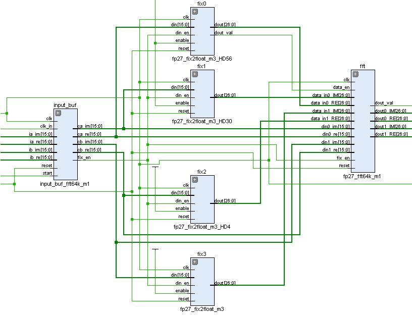
In the structure of the implemented FFT node, 3 functional nodes can be distinguished: data conversion from integer type to a special floating point format, an input buffer for recording signal samples, and an FFT core, which contains various complete special purpose nodes.
Schematic view of the synthesized project: Input buffer + FP converters + FFT Core
To increase efficiency, all calculations are performed in a special 23-bit floating-point format FP23. This is a progressive implementation of the FP18 and FP27 algorithms, on the basis of which all the logic is built. The following features are characteristic of the FP23 format: the word width is 23 bits, the mantissa is 16, the exponents are 6 and the sign is 1. The FP23 format is specially adapted to the FPGA architecture and takes into account the internal features of the operation of crystal blocks such as the DSP48 universal digital processing unit and memory blocks RAMB18. The use of the floating point format ensures high accuracy of signal processing with ADC regardless of their amplitude and allows you to avoid computational errors when scaling data inherent to systems with integer hardware computing with a limitation on the width of the calculations. You can read about it in my previous article .
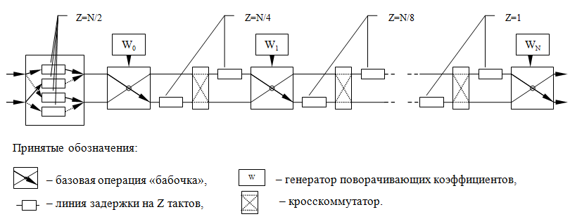
The following figure shows the pipeline FFT calculation scheme for a sequence of length N = 2 ^ n . It contains:
The FFT core conveyor is designed so that the data at its input must come in a natural order , and at the output of the FFT a data stream is formed in a discharge-inverse order . For OBPF, the opposite is true - the input data are in binary-inverse order , and the output in natural or natural order . This is the main advantage of this bundle of FFT and OBFT in comparison with ready-made cores from Xilinx, for which the input data must be strictly in natural order, and the output data depends on the enabled option.
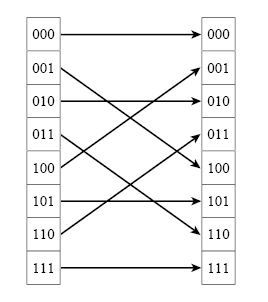
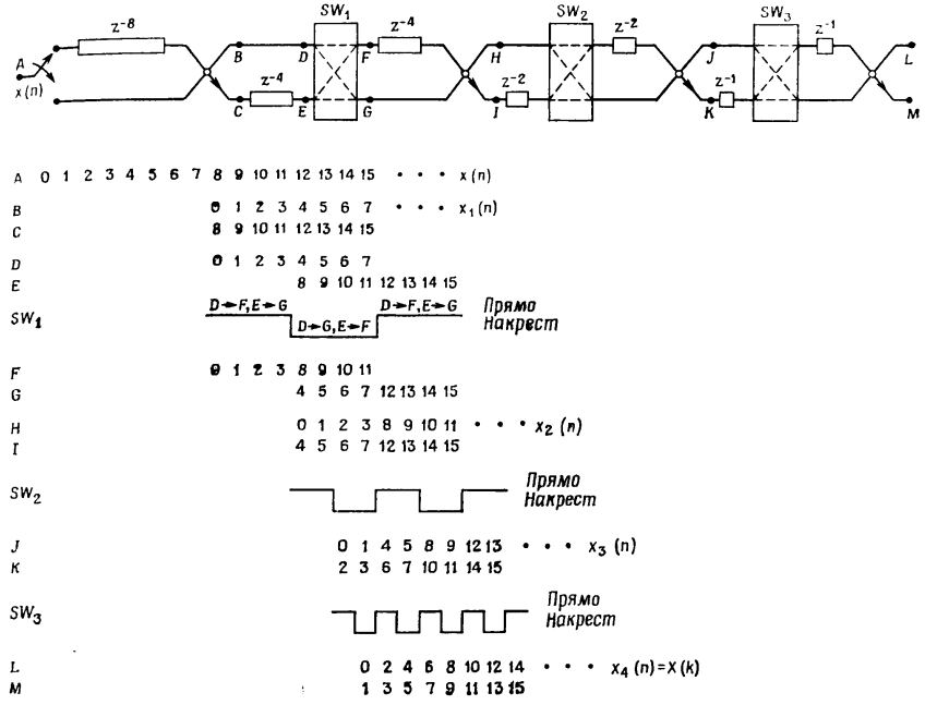
What is a binary-inverse order and how it is obtained from the natural order is clearly demonstrated by the following picture (for a sequence of N = 8 samples):
It is built on the distributed or internal memory of the FPGA crystal. In the latest implementation, it is a memory, at the input of which N complex samples arrive, and at the output two N / 2 packs of samples are formed, and the first pack contains samples [0; N / 2 -1], and in the second bundle [N / 2; N-1]. In fact, the input buffer is the zero delay line for the FFT node and there is a primary permutation of the data in it.
The VHDL source code for implementing buffer memory or delay lines is fairly simple and essentially implements dual-port memory:
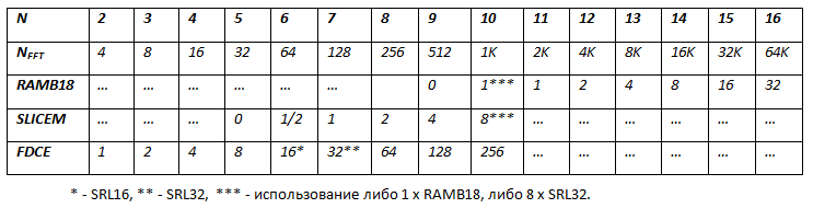
For each stage of the butterfly calculation, a different number of coefficients is needed. For example, for the first stage only 1 coefficient is needed, for the second stage 2, for the third 4, etc. proportional to the power of two. In this regard, the turning factors are implemented on the basis of distributed (SLICEM) and internal (RAMB) FPGA memory in the form of ROM-memory, which stores the sine and cosine counts. For economical storage is used reception, allowing to reduce memory resources. It consists in the fact that with the help of a quarter of the sine and cosine period it is possible to construct the entire period of the harmonic signal using only operations with the sign and direction of the memory address. If necessary, only one eighth of the coefficients can be stored, and the remaining sections can be obtained by switching the data source of harmonic signals between themselves and changing the direction of the counter. In the current implementation, this does not bring performance gains and slightly saves the resource of block memory, and significantly increases the amount of logical resources of the crystal.
Example of cosine shaping:
Simple logic on the multiplexers of the address and data counter allows saving FPGA memory 4 times.
The coefficients are stored in an integer format of 16 bits and after they are retrieved from memory, they are transferred to the FP23 format. I have evaluated performance for floating point and integer format. Practice has shown that the first version saves the crystal memory 1.5 times , while the performance of the entire core does not deteriorate, and the added delay in converting formats at some stages even brings some advantages (leveling the delays with the data and coefficients for the butterfly with frequency decimation).
The rotation coefficients for small FFT lengths are stored in the distributed memory of the FPGA in the SLICEM cells up to the stage when it is necessary to store 512 complex samples with a total capacity of 32 bits. For large FFT lengths, RAMB18 block memory is used, and for storing 1024 pairs of samples, only 2 RAMB18 blocks are needed, which is equivalent to 36 * 1K = 16 * 2 * 1K = 18K * 2. Note that 1024 coefficients are converted to 2048 using the described earlier method of partial data storage, and taking into account the double parallelism Radix-2, it allows you to serve the FFT with a length of NFFT = 4096 samples.
For NFFT FFT lengths> 4096 counts, the expansion of the coefficients in a Taylor series to the first derivative is used, which allows to calculate the turning coefficients with sufficiently high accuracy and save FPGA memory additionally. We omit some theoretical calculations and proceed directly to the practical features of the calculation.
For large values of NFFT, the turning factors are not stored directly in the block memory of the FPGA, but are obtained by calculating using the Taylor method. The calculated formulas for the real and imaginary parts of the turning factors in a simplified form are given below:
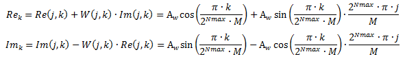
In these formulas:
A w - the amplitude of the turning factors (as a rule, A w = 2 16 ),
2 Nmax - the maximum number of turning factors limiting the use of FPGA block memory (in the current implementation, 2 Nmax = 2048, that is, Nmax = 12),
k is the counter of all coefficient values at the current FFT stage, k = 0 ... 2 Nmax ∙ M-1,
j - counter of intermediate values of the coefficients at the current stage of the FFT, j = 0 ... M-1,
M is a number depending on the stage of calculation, is defined as M = 2 stage , where stage is the number of the FFT stage.
Re k , Im k - calculated values of the turning factors.
The figure shows a simplified scheme for implementing the calculation of coefficients according to the Taylor scheme (the address counter is used to extract coefficients from memory and mathematical operations with data)
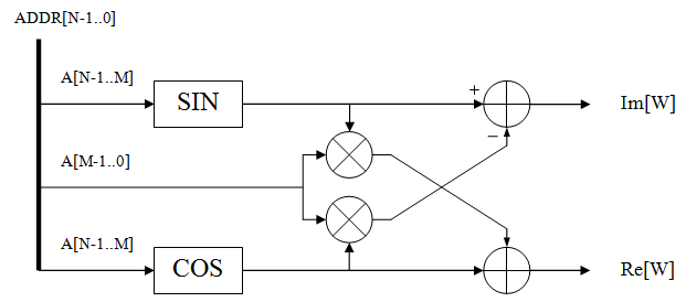
Since the calculations of the turning coefficients are performed using mathematical operations and extracting data from the block memory, each stage of storing the coefficients occupies the resources DSP48 and RAMB18. For the presented calculation formulas, an algorithm was written using 2 operations of multiplying harmonic functions and 1 operation of multiplying by the counter value, which is equivalent to 3 DSP48 blocks.
If the Taylor scheme was not used in the core, then for each next stage the block memory resources would grow proportionally to degree 2. For 4096 samples, 4 RAMB primitives are expended, for 8192 samples - 8 primitives, etc. When using the Taylor algorithm, the number of block memory primitives always remains fixed and equal to 2.
The code for creating the sine and cosine coefficients is based on the VHDL function (you must use the MATH package). The function is synthesized and successfully converts data into a 32-bit data vector in integer format.
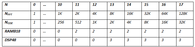
Table of resources for the implementation of turning factors:
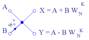
Each butterfly for FFT and OBPF uses 4 multipliers and 6 adders-subtractors, realizing the function of complex multiplication and addition / subtraction. Of the functional blocks presented, only multipliers use DSP48 cells, 1 each. From this it follows that only 4 DSP48 primitives per FFT butterfly. Formulas for calculating butterflies with thinning in frequency and time are given in the sources above. Butterflies are implemented quite simply. Butterfly does not occupy resources of block memory. The pitfall here is simple and easy to manage: you should take into account delays in the calculations in the process of calculating the data and unloading the turning coefficients Wn. For the FFT and OBPF these delays are different!
Cross-switches and delay lines implement data swapping to the required order for each stage of the FFT. The most detailed description of the permutation algorithm is given in the book of Rabiner and Gold ! Use distributed or block memory FPGA. No tricks to save memory here, unfortunately, can not be done. This is the most non-optimizable block and is implemented as it is.
Table of resources for the implementation of delay lines in general:
Let me take a picture from the book, which shows the process of binary rearrangement in the delay lines at different stages for NFFT = 16.
In C ++, this algorithm is implemented as follows:
The butterfly receives the A and B counts with the numbers jN and jN + iN , and the coefficients WW are received with the numbers ii * CNT_jj . For a complete understanding of the process, it is enough to look at the binary permutation scheme and the example from the book.
Further actions are quite simple - all nodes must be correctly connected to each other, taking into account delays in performing various operations (mathematics in butterflies, unloading coefficients for different stages). If everything is done correctly, in the end result you will have a ready-made working core.
The following table shows the resource calculation for the FP23FFTK FFT core and for the Xilinx FFT core (Floating point, Radix-2, Pipelined Streaming I / O options). The table for the Xilinx core contains two columns of resources for block memory: (1) - without converting the order from binary inverse to natural ( bitreverse output data ) and (2) - with conversion ( natural output data ).
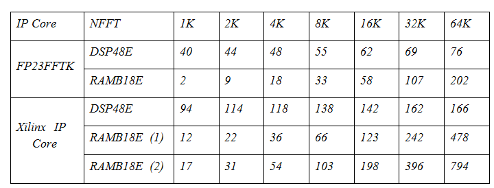
As can be seen from the table, the FP23FFTK core is 2.5 times smaller than the DSP48 primitives with NFFT = 64K, which is primarily due to the format of the data with the reduced mantissa and the exponent (FP23 vs FP32). In addition, the kernel takes 2.5 times less than the components of the block memory for the bitreverse option and 4 times less for the natural option in the Xilinx core. This can be justified by a truncated data format, but it gives a gain of only 1.5 times. The remaining improvements are related to the storage characteristics of the turning factors and the use of the Taylor algorithm.
Example: the Xilinx FFT core must accept input data in its natural order ( kernel feature! ), Therefore, for the FFT + OBPF bundle of Xilinx cores with NFFT = 64K, ~ 1600 block memory cells will be required, and for the same bundle in FP23FFTK format only ~ 400 cells RAMB, since OBPF is not required to translate data into a natural form, and at its output data is already in kind. This feature allows you to build compact compression filters (a bunch of FFT + OBPF) on fast convolutions in small FPGA crystals without loss of performance!
Below is the log of FFT core synthesis for NFFT = 65536 points:

Due to the fact that I am limited in iron, the FFT core was tested only on two crystals: Virtex-6 (XC6VSX315T) and Kintex-7 (XC7K325T).
For the FFT + OBPF bundle with NFFT = 64K counts on Xilinx FPGA Virtex-6 SX315T, it was possible to achieve stable filter operation at a frequency F dsp = 333 MHz . The Xilinx FFT core also worked at this frequency, but the amount of resources occupied was significantly higher.
For the Kintex-7 FPGA, a stable multichannel circuit with independent filters is implemented with NFFT = 8K, the processing frequency is also equal to F dsp = 333 MHz .
Unfortunately, at frequencies above 333 MHz and on the FPGA of other families, the operation of the nodes was not checked.
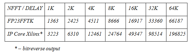
The table below shows the delays in cycles from the input to the kernel output (the full calculation of a packet of NFFT samples) for different FFT lengths. As can be seen from the table, for Xilinx and here the results are disappointing. With the help of the FP23FFTK kernel, it was possible to reduce the time for a complete FFT calculation by ~ 2.5 times ! And if you also include a translation in the natural order in IP Xilinx, then the values will be even greater.
1. 4 channels direct FFT. FPGA: Virtex-6 SX315T (~ 1300 RAMB, ~ 1400 DSP48). 4x FP23FFTK, NFFT = 16K
For the simulation and debugging of the FFT core in floating point format on the FPGA, various development tools were used.
A) Testing of the RTL-model of the FFT core was carried out using Xilinx Vivado and Aldec Active-HDL CAD systems. Despite the high performance of Vivado, it has several drawbacks, one of which is poor code editing tools. It seems that the product is constantly evolving, but some useful gadgets are still missing in the program, so the source code is written in Notepad ++, configured to work with VHDL / Verilog files. Unlike Vivado, Active-HDL models much faster, and also allows you to save time diagrams after exiting the application. Modelsim was not used for lack of license :)
B) Testing of the software model of the FFT core was carried out in Microsoft Visual Studio, for which an application was written in C ++ that repeated the RTL model, but without delays and clock frequencies, which made it possible to quickly and effectively debug at different stages of design ( , commutation switching nodes, mathematical operations, the implementation of the Taylor algorithm and the complete core FFT).
C) Full testing was carried out in Matlab / GNU Octave. Scripts with various test signals were created for debugging, but the simplest chirp signal with different deviation, amplitude, offset, and other parameters turned out to be ideal for visual modeling. It allows you to check the performance of the FFT in the whole part of the spectrum, in contrast to the harmonic signals. When testing with sinusoidal signals, I fell into the trap several times, which is eliminated by the use of the chirp signal. If I apply a sinusoidal signal of a certain frequency to the FFT input, then at the output I get a good harmonic at the desired frequency, but as soon as I change the period of the input sinusoid, errors occurred. The nature of these errors in the process of debugging the RTL code was not easy to trace, but then I found the answer: incorrect delays in the butterfly nodes and turning factors at some stages of the calculations. The use of the chirp signal eliminated this problem and allowed us to select the correct delays at each stage of the FFT calculation. Also, using m-scripts, we compared the work of C ++ and RTL-models, and also checked the difference in calculations in the FP23 floating-point format and in the float / double format.
This process may seem somewhat routine, but it was in this sequence that I managed to ensure the correct operation of all the FFT nodes. It may also help you if you use the kernel in your projects.
1. Run the Matlab / Octave script to create a reference signal. You can control the following variables:
As a result, two files are created (for the real and imaginary components), which are used in C ++ and RTL models.
2. Create a project in Microsoft Visual Studio, taking the source code in C ++ in the appropriate directory.
3. Build and run the project. You can set the following variables in the h-file:
4. Create an HDL project in a Vivado or Active-HDL environment, taking the source files to VHDL.
5. Run the simulation using a file from the testbench directory. You can set the following options in this file:
6. Re-run the m-script (from item 1) to test the operation of the C ++ / RTL cores of the FFT and OBPF.
After these magical actions are carried out, the graph of the input signal and the graphs of the signal passing through the FFT and OBPF nodes will be reflected on the screen. To test only one FFT node, you need to take another m-script from the math directory and make some changes to the source files.
Visual inspection of C ++ and RTL models (a bunch of FFT + OBPF):
All FP23FFTK FFT core kernel sources on VHDL (including basic operations in FP23 format), the C ++ test model and Matlab / Octave m-scripts are available in my github profile .
Of course, the development of the project does not end there. In my plans on the basis of already created models to make a lot of interesting and new, for example:
, . Xilinx FP23FFTK , , , . , FP23FFTK , !
( , ). , , , . , . , — . , ++ , .
, - . ( , FP23 ..). dsmv2014 , .
Thanks for attention!
Introduction
In digital signal processing, without any doubt, the main analysis tool is the Fast Fourier Transform (FFT). The algorithm is used in almost all areas of science and technology. The simplest physical example of the Fourier transform is the human perception of sound. Whenever we hear a sound, the auricle automatically performs a complex calculation, which a person is able to do only after several years of studying math. The essence of the phenomenon lies in the fact that the auditory organ represents sound in the form of a spectrum of consecutive loudness values for tones of different heights, and the brain transforms the received information into perceived sound.
In matters of radio engineering, FFT algorithms are used in convolutions and in the design of digital correlators, used in image processing, as well as in audio and video equipment (equalizers, spectrum analyzers, vocoders). In addition, FFT methods underlie all sorts of data encryption and compression algorithms (jpeg, mpeg4, mp3), as well as when working with long numbers. FFT is used in sonar systems to detect surface ships and submarines, and in radar systems to obtain information about speed, flight direction and distance to targets.
')
Various FFT modules are available in almost any application package for research, such as Maple, MATLAB, GNU Octave, MathCAD, Mathematica. The specialist must understand the Fourier transform process and be able to correctly apply it to solve the set tasks, where necessary.
The first software implementation of the FFT algorithm was carried out in the early 60s of the 20th century at the IBM Computing Center by John Cooley under the direction of John Tukey. In 1965 they also published an article devoted to the fast Fourier transform algorithm. This method formed the basis of many FFT algorithms and was named after the developers - Cooley-Tukey. Since then, quite a lot of various publications and monographs have been issued, in which various methods and algorithms of FFT are developed and described, reducing the number of operations performed, reducing energy costs and resources, etc. Today, FFT is not the name of one, but a large number of different algorithms designed to quickly calculate the Fourier transform.
Theory
I will not describe in detail the theory from the course of the radio engineering faculty of the type “Digital signal processing”. Instead, I will provide a selection of the most useful sources, where you can get acquainted with both theoretical research and practical calculations and implementation features of various FFT algorithms.
Articles on Habré:
- Simple words about Fourier transform
- Practical application of Fourier transform
- Fourier transform in action ...
- Fourier processing of digital images
- Matlab and Fast Fourier Transform
- Spectral analysis of signals
Books:
- E.S. Ifcher, Barry U. Dervis., Digital Signal Processing. Practical approach
- Rabiner L., Gold B., Theory and application of digital signal processing
DSPLIB website:
- Time thinning FFT
- FFT with thinning by frequency
- Fast Fourier transform. Principle of construction
- Polyphase FFT
Algorithm
The FFT node is made according to the Kuli-Tuki algorithm with base 2. All calculations for such an implementation are reduced to the repeated execution of the basic operation “butterfly”. The transformation method is based on a conveyor scheme with frequency thinning (for FFT) and temporary thinning (for IFFT). The algorithm uses a scheme of double parallelism. This approach allows the processing of a continuous stream of complex samples from the ADC, the sampling frequency of which is 2 times higher than the processing clock frequency. That is, the FFT “butterfly” performs a calculation for two complex samples at the same time. If 4 or 8 times parallelism is used, then the data stream from the ADC or any other source can be processed at a frequency 4 and 8 times higher than the processing frequency. Such schemes are often used in problems of the polyphase Fourier transform (Polyphase FFT) and are of particular interest.
To save RAMB memory in the FPGA chip, starting from a certain stage of the FFT (at NFFT> 4096 points), linear interpolation of the turning coefficients is used - decomposition into a Taylor series to the first derivative. This allows instead of storing the entire set of coefficients to use only a part of them, and the rest to be obtained by approximate calculation from the original set. By sacrificing the resources of the DSP48 primitives, the resources of the block RAMB are saved, which for FFT nodes is a critical place in any hardware implementation on the FPGA. More on this will be discussed below.
Structural scheme
In the structure of the implemented FFT node, 3 functional nodes can be distinguished: data conversion from integer type to a special floating point format, an input buffer for recording signal samples, and an FFT core, which contains various complete special purpose nodes.
Schematic view of the synthesized project: Input buffer + FP converters + FFT Core
To increase efficiency, all calculations are performed in a special 23-bit floating-point format FP23. This is a progressive implementation of the FP18 and FP27 algorithms, on the basis of which all the logic is built. The following features are characteristic of the FP23 format: the word width is 23 bits, the mantissa is 16, the exponents are 6 and the sign is 1. The FP23 format is specially adapted to the FPGA architecture and takes into account the internal features of the operation of crystal blocks such as the DSP48 universal digital processing unit and memory blocks RAMB18. The use of the floating point format ensures high accuracy of signal processing with ADC regardless of their amplitude and allows you to avoid computational errors when scaling data inherent to systems with integer hardware computing with a limitation on the width of the calculations. You can read about it in my previous article .
The following figure shows the pipeline FFT calculation scheme for a sequence of length N = 2 ^ n . It contains:
- Input buffer - performs the initial data preparation at the FFT input (permutation of the samples, depending on the implementation and the used ADC scheme),
- Rotation coefficients generators - nodes of distributed and block memory, in which sine and cosine counts are stored,
- The butterfly is the basic operation of the FFT core (with frequency and time decimation),
- Delay lines and cross -connectors — provide the input of “butterflies” of elements of the array being processed with the necessary indices.
The FFT core conveyor is designed so that the data at its input must come in a natural order , and at the output of the FFT a data stream is formed in a discharge-inverse order . For OBPF, the opposite is true - the input data are in binary-inverse order , and the output in natural or natural order . This is the main advantage of this bundle of FFT and OBFT in comparison with ready-made cores from Xilinx, for which the input data must be strictly in natural order, and the output data depends on the enabled option.
What is a binary-inverse order and how it is obtained from the natural order is clearly demonstrated by the following picture (for a sequence of N = 8 samples):
Input buffer
It is built on the distributed or internal memory of the FPGA crystal. In the latest implementation, it is a memory, at the input of which N complex samples arrive, and at the output two N / 2 packs of samples are formed, and the first pack contains samples [0; N / 2 -1], and in the second bundle [N / 2; N-1]. In fact, the input buffer is the zero delay line for the FFT node and there is a primary permutation of the data in it.
The VHDL source code for implementing buffer memory or delay lines is fairly simple and essentially implements dual-port memory:
PR_RAMB: process(clk) is begin if (clk'event and clk = '1') then if (enb = '1') then ram_dout <= ram(conv_integer(addrb)); end if; if (ena = '1') then if (wea = '1') then ram(conv_integer(addra)) <= ram_din; end if; end if; end if; end process; Rotation coefficients generators
For each stage of the butterfly calculation, a different number of coefficients is needed. For example, for the first stage only 1 coefficient is needed, for the second stage 2, for the third 4, etc. proportional to the power of two. In this regard, the turning factors are implemented on the basis of distributed (SLICEM) and internal (RAMB) FPGA memory in the form of ROM-memory, which stores the sine and cosine counts. For economical storage is used reception, allowing to reduce memory resources. It consists in the fact that with the help of a quarter of the sine and cosine period it is possible to construct the entire period of the harmonic signal using only operations with the sign and direction of the memory address. If necessary, only one eighth of the coefficients can be stored, and the remaining sections can be obtained by switching the data source of harmonic signals between themselves and changing the direction of the counter. In the current implementation, this does not bring performance gains and slightly saves the resource of block memory, and significantly increases the amount of logical resources of the crystal.
Example of cosine shaping:
- First quarter: counter address +1, counts cos,
- Second quarter: +1 address counter, -sin counts,
- Third quarter: address counter -1, count -sin,
- Fourth quarter: address counter -1, cos counts,
Simple logic on the multiplexers of the address and data counter allows saving FPGA memory 4 times.
The coefficients are stored in an integer format of 16 bits and after they are retrieved from memory, they are transferred to the FP23 format. I have evaluated performance for floating point and integer format. Practice has shown that the first version saves the crystal memory 1.5 times , while the performance of the entire core does not deteriorate, and the added delay in converting formats at some stages even brings some advantages (leveling the delays with the data and coefficients for the butterfly with frequency decimation).
The rotation coefficients for small FFT lengths are stored in the distributed memory of the FPGA in the SLICEM cells up to the stage when it is necessary to store 512 complex samples with a total capacity of 32 bits. For large FFT lengths, RAMB18 block memory is used, and for storing 1024 pairs of samples, only 2 RAMB18 blocks are needed, which is equivalent to 36 * 1K = 16 * 2 * 1K = 18K * 2. Note that 1024 coefficients are converted to 2048 using the described earlier method of partial data storage, and taking into account the double parallelism Radix-2, it allows you to serve the FFT with a length of NFFT = 4096 samples.
For NFFT FFT lengths> 4096 counts, the expansion of the coefficients in a Taylor series to the first derivative is used, which allows to calculate the turning coefficients with sufficiently high accuracy and save FPGA memory additionally. We omit some theoretical calculations and proceed directly to the practical features of the calculation.
For large values of NFFT, the turning factors are not stored directly in the block memory of the FPGA, but are obtained by calculating using the Taylor method. The calculated formulas for the real and imaginary parts of the turning factors in a simplified form are given below:
In these formulas:
A w - the amplitude of the turning factors (as a rule, A w = 2 16 ),
2 Nmax - the maximum number of turning factors limiting the use of FPGA block memory (in the current implementation, 2 Nmax = 2048, that is, Nmax = 12),
k is the counter of all coefficient values at the current FFT stage, k = 0 ... 2 Nmax ∙ M-1,
j - counter of intermediate values of the coefficients at the current stage of the FFT, j = 0 ... M-1,
M is a number depending on the stage of calculation, is defined as M = 2 stage , where stage is the number of the FFT stage.
Re k , Im k - calculated values of the turning factors.
The figure shows a simplified scheme for implementing the calculation of coefficients according to the Taylor scheme (the address counter is used to extract coefficients from memory and mathematical operations with data)
Since the calculations of the turning coefficients are performed using mathematical operations and extracting data from the block memory, each stage of storing the coefficients occupies the resources DSP48 and RAMB18. For the presented calculation formulas, an algorithm was written using 2 operations of multiplying harmonic functions and 1 operation of multiplying by the counter value, which is equivalent to 3 DSP48 blocks.
If the Taylor scheme was not used in the core, then for each next stage the block memory resources would grow proportionally to degree 2. For 4096 samples, 4 RAMB primitives are expended, for 8192 samples - 8 primitives, etc. When using the Taylor algorithm, the number of block memory primitives always remains fixed and equal to 2.
The code for creating the sine and cosine coefficients is based on the VHDL function (you must use the MATH package). The function is synthesized and successfully converts data into a 32-bit data vector in integer format.
function rom_twiddle(xx : integer) return std_array_32xN is variable pi_new : real:=0.0; variable re_int : integer:=0; variable im_int : integer:=0; variable sc_int : std_array_32xN; begin for ii in 0 to 2**(xx-1)-1 loop pi_new := (real(ii) * MATH_PI)/(2.0**xx); re_int := INTEGER(32768.0*COS( pi_new)); im_int := INTEGER(32768.0*SIN(-pi_new)); sc_int(ii)(31 downto 16) := STD_LOGIC_VECTOR(CONV_SIGNED(im_int, 16)); sc_int(ii)(15 downto 00) := STD_LOGIC_VECTOR(CONV_SIGNED(re_int, 16)); end loop; return sc_int; end rom_twiddle; Table of resources for the implementation of turning factors:
Butterfly
Each butterfly for FFT and OBPF uses 4 multipliers and 6 adders-subtractors, realizing the function of complex multiplication and addition / subtraction. Of the functional blocks presented, only multipliers use DSP48 cells, 1 each. From this it follows that only 4 DSP48 primitives per FFT butterfly. Formulas for calculating butterflies with thinning in frequency and time are given in the sources above. Butterflies are implemented quite simply. Butterfly does not occupy resources of block memory. The pitfall here is simple and easy to manage: you should take into account delays in the calculations in the process of calculating the data and unloading the turning coefficients Wn. For the FFT and OBPF these delays are different!
Delay lines
Cross-switches and delay lines implement data swapping to the required order for each stage of the FFT. The most detailed description of the permutation algorithm is given in the book of Rabiner and Gold ! Use distributed or block memory FPGA. No tricks to save memory here, unfortunately, can not be done. This is the most non-optimizable block and is implemented as it is.
Table of resources for the implementation of delay lines in general:
Let me take a picture from the book, which shows the process of binary rearrangement in the delay lines at different stages for NFFT = 16.
In C ++, this algorithm is implemented as follows:
for (int cnt=1; cnt<stages+1; cnt++) { int CNT_ii = pow(2.0,(stFFT-cnt)); int CNT_jj = pow(2.0,(cnt-1)); for (int jj=0; jj<CNT_jj; jj++) { for (int ii=0; ii<CNT_ii; ii++) { int jN = ii+jj*(N_FFT/pow(2.0,cnt-1)); int iN = N_FFT/(pow(2.0,cnt)); int xx = jj*N_FFT/pow(2.0,cnt); // mix data // -------- A, B, WW, IND[A], IND[B], IND[W] -------- // ButterflyFP(Ax, Bx, CFW, jN, jN+iN, ii*CNT_jj); } } } The butterfly receives the A and B counts with the numbers jN and jN + iN , and the coefficients WW are received with the numbers ii * CNT_jj . For a complete understanding of the process, it is enough to look at the binary permutation scheme and the example from the book.
Total resources
Further actions are quite simple - all nodes must be correctly connected to each other, taking into account delays in performing various operations (mathematics in butterflies, unloading coefficients for different stages). If everything is done correctly, in the end result you will have a ready-made working core.
The following table shows the resource calculation for the FP23FFTK FFT core and for the Xilinx FFT core (Floating point, Radix-2, Pipelined Streaming I / O options). The table for the Xilinx core contains two columns of resources for block memory: (1) - without converting the order from binary inverse to natural ( bitreverse output data ) and (2) - with conversion ( natural output data ).
As can be seen from the table, the FP23FFTK core is 2.5 times smaller than the DSP48 primitives with NFFT = 64K, which is primarily due to the format of the data with the reduced mantissa and the exponent (FP23 vs FP32). In addition, the kernel takes 2.5 times less than the components of the block memory for the bitreverse option and 4 times less for the natural option in the Xilinx core. This can be justified by a truncated data format, but it gives a gain of only 1.5 times. The remaining improvements are related to the storage characteristics of the turning factors and the use of the Taylor algorithm.
Example: the Xilinx FFT core must accept input data in its natural order ( kernel feature! ), Therefore, for the FFT + OBPF bundle of Xilinx cores with NFFT = 64K, ~ 1600 block memory cells will be required, and for the same bundle in FP23FFTK format only ~ 400 cells RAMB, since OBPF is not required to translate data into a natural form, and at its output data is already in kind. This feature allows you to build compact compression filters (a bunch of FFT + OBPF) on fast convolutions in small FPGA crystals without loss of performance!
Below is the log of FFT core synthesis for NFFT = 65536 points:
Core performance
Due to the fact that I am limited in iron, the FFT core was tested only on two crystals: Virtex-6 (XC6VSX315T) and Kintex-7 (XC7K325T).
For the FFT + OBPF bundle with NFFT = 64K counts on Xilinx FPGA Virtex-6 SX315T, it was possible to achieve stable filter operation at a frequency F dsp = 333 MHz . The Xilinx FFT core also worked at this frequency, but the amount of resources occupied was significantly higher.
For the Kintex-7 FPGA, a stable multichannel circuit with independent filters is implemented with NFFT = 8K, the processing frequency is also equal to F dsp = 333 MHz .
Unfortunately, at frequencies above 333 MHz and on the FPGA of other families, the operation of the nodes was not checked.
The table below shows the delays in cycles from the input to the kernel output (the full calculation of a packet of NFFT samples) for different FFT lengths. As can be seen from the table, for Xilinx and here the results are disappointing. With the help of the FP23FFTK kernel, it was possible to reduce the time for a complete FFT calculation by ~ 2.5 times ! And if you also include a translation in the natural order in IP Xilinx, then the values will be even greater.
Implementation examples on FPGAs
1. 4 channels direct FFT. FPGA: Virtex-6 SX315T (~ 1300 RAMB, ~ 1400 DSP48). 4x FP23FFTK, NFFT = 16K
Other examples ...
2. 8 channels of compression (FFT + OBPF). FPGA: Virtex-6 SX315T (~ 1300 RAMB, ~ 1400 DSP48). 16x FP23FFTK, NFFT = 16K

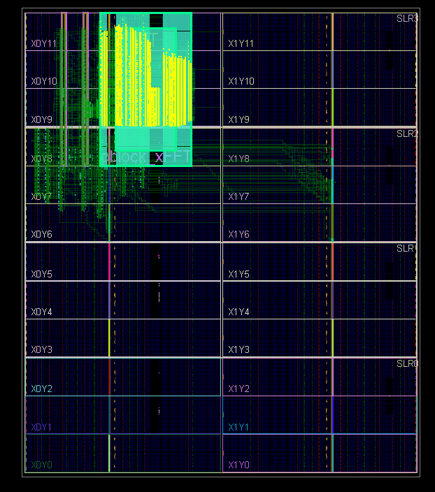
3. FFT + OBPF 64K (large compression filter). FPGA: XC7VX1140TFLG-2 (~ 3700 RAMB, ~ 3600 DSP48).
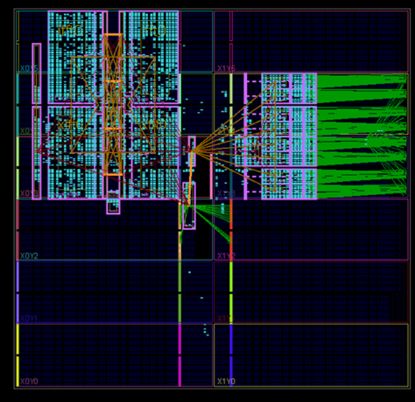
4. Picture of random FFT layout (resembles a butterfly):
3. FFT + OBPF 64K (large compression filter). FPGA: XC7VX1140TFLG-2 (~ 3700 RAMB, ~ 3600 DSP48).
4. Picture of random FFT layout (resembles a butterfly):
Kernel check
For the simulation and debugging of the FFT core in floating point format on the FPGA, various development tools were used.
A) Testing of the RTL-model of the FFT core was carried out using Xilinx Vivado and Aldec Active-HDL CAD systems. Despite the high performance of Vivado, it has several drawbacks, one of which is poor code editing tools. It seems that the product is constantly evolving, but some useful gadgets are still missing in the program, so the source code is written in Notepad ++, configured to work with VHDL / Verilog files. Unlike Vivado, Active-HDL models much faster, and also allows you to save time diagrams after exiting the application. Modelsim was not used for lack of license :)
B) Testing of the software model of the FFT core was carried out in Microsoft Visual Studio, for which an application was written in C ++ that repeated the RTL model, but without delays and clock frequencies, which made it possible to quickly and effectively debug at different stages of design ( , commutation switching nodes, mathematical operations, the implementation of the Taylor algorithm and the complete core FFT).
C) Full testing was carried out in Matlab / GNU Octave. Scripts with various test signals were created for debugging, but the simplest chirp signal with different deviation, amplitude, offset, and other parameters turned out to be ideal for visual modeling. It allows you to check the performance of the FFT in the whole part of the spectrum, in contrast to the harmonic signals. When testing with sinusoidal signals, I fell into the trap several times, which is eliminated by the use of the chirp signal. If I apply a sinusoidal signal of a certain frequency to the FFT input, then at the output I get a good harmonic at the desired frequency, but as soon as I change the period of the input sinusoid, errors occurred. The nature of these errors in the process of debugging the RTL code was not easy to trace, but then I found the answer: incorrect delays in the butterfly nodes and turning factors at some stages of the calculations. The use of the chirp signal eliminated this problem and allowed us to select the correct delays at each stage of the FFT calculation. Also, using m-scripts, we compared the work of C ++ and RTL-models, and also checked the difference in calculations in the FP23 floating-point format and in the float / double format.
Testing algorithm
This process may seem somewhat routine, but it was in this sequence that I managed to ensure the correct operation of all the FFT nodes. It may also help you if you use the kernel in your projects.
1. Run the Matlab / Octave script to create a reference signal. You can control the following variables:
- NFFT is the FFT / OBPF length, the number of transform points,
- Asig - input signal amplitude (0-32767),
- Fsig is the frequency of the input signal,
- F0 is the initial chirp frequency (signal phase),
- Fm is the frequency of the chirp signal envelope (for a non-rectangular envelope),
As a result, two files are created (for the real and imaginary components), which are used in C ++ and RTL models.
2. Create a project in Microsoft Visual Studio, taking the source code in C ++ in the appropriate directory.
3. Build and run the project. You can set the following variables in the h-file:
- NFFT is the length of the FFT / OBPF (depends on the choice in claim 1),
- SCALE is a scaling factor that determines the range of numbers after converting data from the FP23 format to the INT16 format. Values range from 0 to 0x3F.
- _TAY (0/1) - use the calculation of coefficients using the Taylor algorithm (for NFFT> 4096).
4. Create an HDL project in a Vivado or Active-HDL environment, taking the source files to VHDL.
5. Run the simulation using a file from the testbench directory. You can set the following options in this file:
- NFFT is the length of the FFT / OBPF (depends on the choice in claim 1),
- SCALE is a scaling factor that determines the range of numbers after converting data from the FP23 format to the INT16 format. Values range from 0 to 0x3F.
- USE_SCALE (TRUE / FALSE) - use the calculation of the coefficients by the Taylor algorithm or the calculation of the coefficients directly (for NFFT> 4096). The return value for the _TAY variable from p.3.
- USE_FLY_FFT (TRUE / FALSE) - use of butterflies in the FFT core. For debugging purposes, the option has remained, it does not carry any practical benefits.
- USE_FLY_IFFT (TRUE / FALSE) - the use of butterflies in the OBPF core.
6. Re-run the m-script (from item 1) to test the operation of the C ++ / RTL cores of the FFT and OBPF.
After these magical actions are carried out, the graph of the input signal and the graphs of the signal passing through the FFT and OBPF nodes will be reflected on the screen. To test only one FFT node, you need to take another m-script from the math directory and make some changes to the source files.
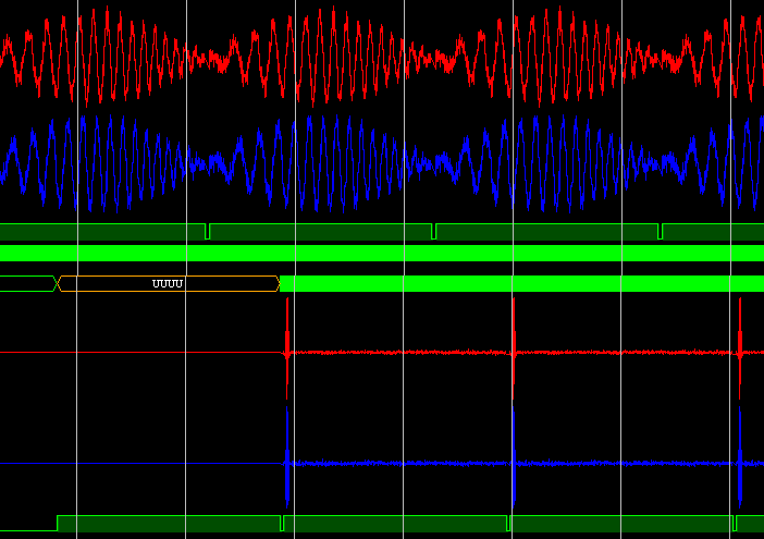
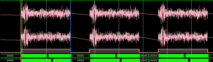
Visual inspection of C ++ and RTL models (a bunch of FFT + OBPF):
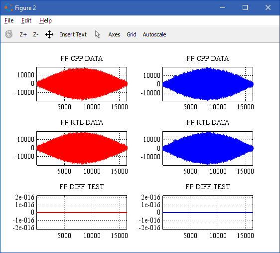
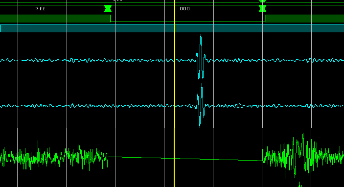
FFT core test results
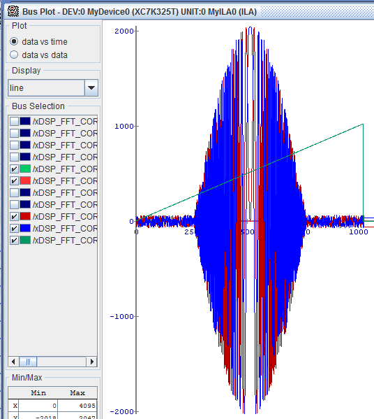
White Noise Chirp Test (Vivado Model)
FFT input:
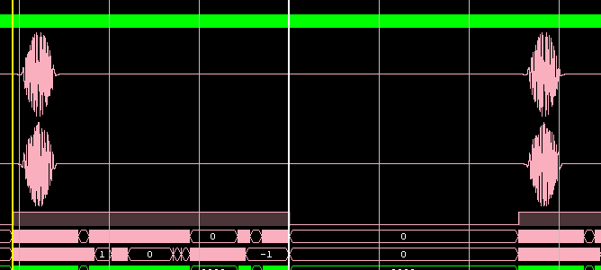
Another test example (input signal and FFT result):
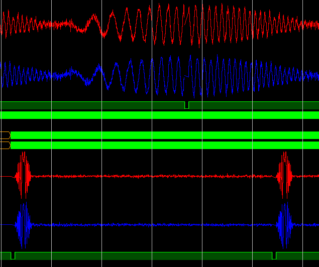
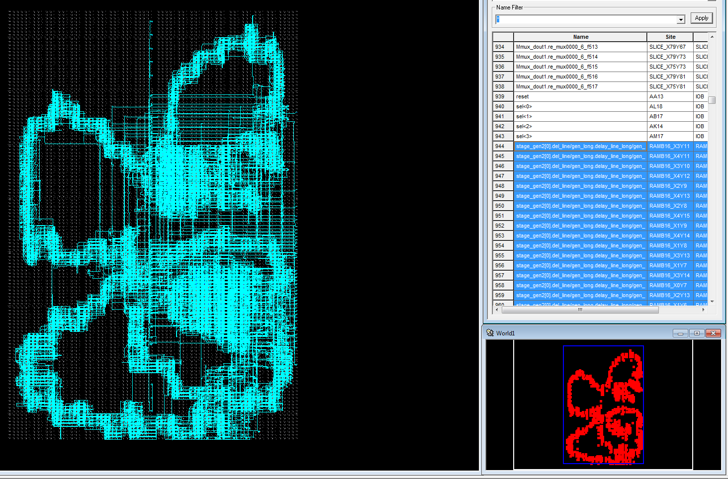
Testing in hardware (debugging in ChipScope) on the Kintex-7 FPGA:
The filter operation is a compressed chirp pulse (there is no compression filter in the source codes of the implementation):
FFT input:
Another test example (input signal and FFT result):
Testing in hardware (debugging in ChipScope) on the Kintex-7 FPGA:
The filter operation is a compressed chirp pulse (there is no compression filter in the source codes of the implementation):
Features of the FFT core FP23FFTK
- Implementation at the level of gates and primitives Xilinx.
- Description Language - VHDL.
- NFFT transform length = 8-256K points.
- Flexible adjustment of NFFT conversion length.
- The specialized format of numbers in floating point is FP23, (the bit width of the mantissa is 16 bits).
- Scale output when converting to fixed point format.
- Compact storage of turning factors through expansion in a Taylor series to the first derivative.
- Storage of a quarter of the period of the coefficients in the distributed and block memory.
- Butterfly for FFT - time decimation, for OBPF - by frequency.
- FFT: input data - in the direct order, at the output in binary inverse.
- OBPF: input data in binary-inverse order, output - in the forward.
- Conveyor processing scheme with double parallelism. Radix-2
- The minimum data burst is NFFT samples in continuous or block mode.
- High computation speed and small amount of resources.
- Significantly shorter delay time for full computation relative to existing cores.
- Implementation on the last FPGA crystals (Virtex-6, 7-Series, Ultrascale)
- No need for expensive bitreverse operation for FFT + OBPF bundle
- Open source.
Source
All FP23FFTK FFT core kernel sources on VHDL (including basic operations in FP23 format), the C ++ test model and Matlab / Octave m-scripts are available in my github profile .
Future plans
Of course, the development of the project does not end there. In my plans on the basis of already created models to make a lot of interesting and new, for example:
- To increase the accuracy of calculations for large FFT lengths, implement the FP32 format (similar to IEEE-754), taking into account the FPGA features, the mantissa length is 25 bits.
- The FFT and OBPF nodes in the FP32 format, the length of NFFT = 256K and higher using the example of a compression filter.
- Polyphase FFT according to the scheme Radix-4, Radix-8, which will allow in the pipeline mode to process data streams from the ADC at very high frequencies.
- Ultra-long FFT scheme (based on 2D-FFT) using external memory for NFFT = 1M-256M points.
Rewrite source files on SystemVerilog.Whether it is necessary?
Conclusion
, . Xilinx FP23FFTK , , , . , FP23FFTK , !
( , ). , , , . , . , — . , ++ , .
, - . ( , FP23 ..). dsmv2014 , .
Thanks for attention!
Source: https://habr.com/ru/post/322728/
All Articles