Primitives for implementing 1-Wire master using PWM and ICP on AVR AtMega microcontrollers
If someone used the linux driver of the 1-Wire bus based on GPIO, he probably noticed that at the time of exchanging data, the loading of SY% jumps to almost 100% (which is quite logical for a bitbang implementation). Of course, you can install a dedicated 1-Wire bus controller connected via I2C DS28E17 or use a UART , but ... Still, using linux for real-time applications is not a good idea. Let the controller on it is engaged in high-level logic, and the whole realtime can be transferred to a separate processor. Moreover, there are more than enough tasks for this separate processor in my project.
No,I will not take STM32 that is now ramping up (after all, I did an implementation for STM8 ). Take the good old AtMega328P (well, or some Arduino , if it becomes easier for someone like this) and collect everything on it. But we will do everything “in an adult way”, with work in the mode of allowed interrupts and with the expectation of the subsequent implementation of higher levels using protothreads (for the protothreads themselves, see the original and chewed examples in Russian ). Those. from bitbang we refuse immediately and irrevocably.
We will also save the UART for future use under other peripherals. For in our case, it is one, and I would have to push the eBus protocol here. For this is also realtime.
I2C is good, but this is another not the cheapest crystal with strapping, and we need it? So, from interesting remains PWM and ICP.
What is PWM, I think, no need to explain. This is simply the generation of pulses of a given phase and duration, which is produced by hardware (that is, from the point of view of the program “in the background”), but the parameters of which can be changed by software. But ICP is quite an interesting thing: it allows the hardware to save the timer value at the moment of changing the signal level at a certain microcontroller output. Thus, it is possible to quite accurately obtain the moment of the occurrence of the event (change in the state of the microcontroller's output) and / or measure its duration.
')
So, we will use hardware TIMER1 ATmega328 (my timers 0 and 2 are used for other purposes). For PWM, you can use pins OC1A and OC1B. However, OC1B is also used as an SS signal, and I planned to connect the ATmega328 to the target device via the SPI bus. This is convenient from the point of view of upgrading ATmega firmware - we make them with the help of the target device, only one of the CE signals from its SPI controller will be put on the SS Atmega contact, and the other CE signal will be put on the RESET pin. Yes, and with the agreement of exchange rates do not need to mess around. Well, as another argument against the use of OC1B is that on the Arduino MEGA 2560 board, this signal is not output to the outside world at all.
So, to generate PWM use the contact OC1A. There are no options for ICP at all - there is only one output of this type for this chip. For the “ACTIVE PULLUP” mode, use any free IO port and configure it to work in the “OUT” mode.
So, with the circuitry sorted out. Now let's refresh the physics of the 1-wire bus. In a nutshell, it can be described as:
Well, then choose the Phase Correct PWM Mode mode (the meter first counts up from the BOTTOM value to the TOP value, and after reaching the TOP value it starts counting down to the BOTTOM value). In this case, the BOTTOM value is fixed and is always 0, and the TOP value can be either one of the fixed values (0xFF, 0x1FF, 0x3FF), or a value from the OCR1A or ICR1 registers. The last two options do not suit us, because OCR1A will be used to generate pulses on the OC1A pin, and ICR1 will be used to measure the low level duration on the 1-Wire bus. Those. it only remains to use the variant with fixed TOP values, since the time interval between bits is not critical for us.
In accordance with the scheme, the OC1A output is enabled in the inverse mode (i.e., a high level setting on it will result in a low level setting on the 1-Wire bus and vice versa), we will use the following PWM mode:

The rest is simple. The new value (the duration of the next transmitted bit) in the OCR1A register will be loaded via the TIMER1_OVF interrupt (in this mode it is generated when the counter reaches the BOTTOM value, and then activated after the TOP value is reached), and the TIMER1_ICP interrupt will be calculated state of the low level and, depending on this, to conclude that the acceptance of bit "1" or bit "0".
Thus, for each operation of receiving or transmitting one bit, we will generate one OVF interrupt and one ICP interrupt. Accordingly, it would be better to optimize their ISRs, but for now let them be written in C.
Well, we’ll perform the RESET operation for the 1-Wire bus by reprogramming TIMER1 to NORMAL mode (since the RESET pulse and the subsequent possible PRESENCE pulse are long enough, we need to expand the “dynamic range” of the timer. In the NORMAL mode, it is 0xFFFF This is quite enough in our case. Moreover, we will even specifically limit it to the value from the OCR1B register, so that in the absence of devices connected to the 1-Wire bus, we should not wait until the timer reaches 0xFFFF, but abort the operation immediately after reaching the maximum time interval).
Manually counting the timer settings depending on the ATmega clock frequency is moveton (and lazily checking all boundary conditions), so let's make it do the C compiler preprocessor using the fact that we need to have a certain constant F_CPU, the value of which is equal to the clock frequency used in Hertz (unsigned long, i.e. a constant must be defined as either 8000000UL or 16000000UL, otherwise the preprocessor will consider it as an int and lose significant digits).
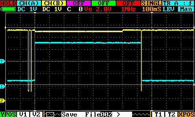
Here is an example of an acquisition waveform:

Channel C is connected to the OC1A output (pulses of the same duration), and channel B is connected to the 1-Wire bus. It can be seen that the duration of the 1st and 3rd pulse on channel B is longer than the duration of the corresponding sync pulse on channel C. Ie The slave in bits 1 and 3 transmits the value "0". And the pulse duration 2 on channels B and C is approximately equal, which corresponds to bit "1".
Since the 1-Wire bus driver used also supports the “ACTIVE PULLUP” mode (which is also implemented in primitives), the corresponding waveforms are listed below:

Activating the “ACTIVE PULLUP” mode after the last bit of the command has been transmitted (the channel B signal goes from low to high, after which the PULLUP activation signal also goes to the active state for no more than 10 µs, applying the supply voltage to the signal bus through Q5).
The same mode is “ACTIVE PULLUP”, but on a smaller scale (command transmission, activation of PULLUP, deactivation of PULLUP and reading command with obtaining results).
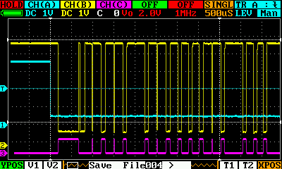
The end of the "ACTIVE PULLUP" mode with the transfer of the command to read the results in an enlarged form.

The RESET procedure (the first low level pulse on channel B, coinciding in duration with the high level pulse on channel C) followed by a PRESENCE from the device connected to the 1-Wire bus (the second low level pulse on channel B, when channel C also has a low level).

The same, but after the end of the mode "ACTIVE PULLUP".
Question to readers: does it make sense to write a sequel, where will the implementation of 1-Wire exchange protocol commands be based on these primitives and the protothreads library ? In principle, everything is very simple there and is written just right away, peeping with one eye into the corresponding datasheet.
Bibliography
No,
We will also save the UART for future use under other peripherals. For in our case, it is one, and I would have to push the eBus protocol here. For this is also realtime.
I2C is good, but this is another not the cheapest crystal with strapping, and we need it? So, from interesting remains PWM and ICP.
What is PWM, I think, no need to explain. This is simply the generation of pulses of a given phase and duration, which is produced by hardware (that is, from the point of view of the program “in the background”), but the parameters of which can be changed by software. But ICP is quite an interesting thing: it allows the hardware to save the timer value at the moment of changing the signal level at a certain microcontroller output. Thus, it is possible to quite accurately obtain the moment of the occurrence of the event (change in the state of the microcontroller's output) and / or measure its duration.
')
So, we will use hardware TIMER1 ATmega328 (my timers 0 and 2 are used for other purposes). For PWM, you can use pins OC1A and OC1B. However, OC1B is also used as an SS signal, and I planned to connect the ATmega328 to the target device via the SPI bus. This is convenient from the point of view of upgrading ATmega firmware - we make them with the help of the target device, only one of the CE signals from its SPI controller will be put on the SS Atmega contact, and the other CE signal will be put on the RESET pin. Yes, and with the agreement of exchange rates do not need to mess around. Well, as another argument against the use of OC1B is that on the Arduino MEGA 2560 board, this signal is not output to the outside world at all.
So, to generate PWM use the contact OC1A. There are no options for ICP at all - there is only one output of this type for this chip. For the “ACTIVE PULLUP” mode, use any free IO port and configure it to work in the “OUT” mode.
So, with the circuitry sorted out. Now let's refresh the physics of the 1-wire bus. In a nutshell, it can be described as:
- Receive and transmit is clocked by the master device (i.e. us)
- The time interval between the transmitted and / or received bits is not critical (the main thing is that it be not less than the minimum allowable)
- The duration of the transmitted pulse and the duration of the received (measured) signal is critical.
Well, then choose the Phase Correct PWM Mode mode (the meter first counts up from the BOTTOM value to the TOP value, and after reaching the TOP value it starts counting down to the BOTTOM value). In this case, the BOTTOM value is fixed and is always 0, and the TOP value can be either one of the fixed values (0xFF, 0x1FF, 0x3FF), or a value from the OCR1A or ICR1 registers. The last two options do not suit us, because OCR1A will be used to generate pulses on the OC1A pin, and ICR1 will be used to measure the low level duration on the 1-Wire bus. Those. it only remains to use the variant with fixed TOP values, since the time interval between bits is not critical for us.
In accordance with the scheme, the OC1A output is enabled in the inverse mode (i.e., a high level setting on it will result in a low level setting on the 1-Wire bus and vice versa), we will use the following PWM mode:
- when the timer counts down and its value coincides with the value from the OCR1A register, we set the signal at the OC1A pin to a high level (there will be a low level on the 1-Wire bus).
- when the timer counts up and its value coincides with the value from the OCR1A register, set the signal at the OC1A pin to a low level (and, perhaps, start measuring the moment of the signal transition at the ICP pin from low to high).
The rest is simple. The new value (the duration of the next transmitted bit) in the OCR1A register will be loaded via the TIMER1_OVF interrupt (in this mode it is generated when the counter reaches the BOTTOM value, and then activated after the TOP value is reached), and the TIMER1_ICP interrupt will be calculated state of the low level and, depending on this, to conclude that the acceptance of bit "1" or bit "0".
Thus, for each operation of receiving or transmitting one bit, we will generate one OVF interrupt and one ICP interrupt. Accordingly, it would be better to optimize their ISRs, but for now let them be written in C.
Well, we’ll perform the RESET operation for the 1-Wire bus by reprogramming TIMER1 to NORMAL mode (since the RESET pulse and the subsequent possible PRESENCE pulse are long enough, we need to expand the “dynamic range” of the timer. In the NORMAL mode, it is 0xFFFF This is quite enough in our case. Moreover, we will even specifically limit it to the value from the OCR1B register, so that in the absence of devices connected to the 1-Wire bus, we should not wait until the timer reaches 0xFFFF, but abort the operation immediately after reaching the maximum time interval).
Manually counting the timer settings depending on the ATmega clock frequency is moveton (and lazily checking all boundary conditions), so let's make it do the C compiler preprocessor using the fact that we need to have a certain constant F_CPU, the value of which is equal to the clock frequency used in Hertz (unsigned long, i.e. a constant must be defined as either 8000000UL or 16000000UL, otherwise the preprocessor will consider it as an int and lose significant digits).
Determine the parameters of the used board
/* Arduino Pro Mini 1-Wire connection */ #define WIRE1_DDR DDRB #define WIRE1_PORT PORTB #define WIRE1_PIN PINB /* OC1A/PCINT1 */ #define WIRE1_OUT PB1 /* (PCINT0/CLKO/ICP1) */ #define WIRE1_ICP PB0 #define WIRE1_IN_ICP PINB0 /* Active pullup PD7 */ #define WIRE1_PULLUP_DDR DDRD #define WIRE1_PULLUP_PORT PORTD #define WIRE1_PULLUP_OUT PD7 /* Presence detection in idle mode: external interrupt #0 */ #define WIRE1_IDLE_PRESENCE_DETECT_IRQ INT0_vect #define WIRE1_IDLE_PRESENCE_DETECT_EICRA_MASK (_BV(ISC01) | _BV(ISC00)) /* Presence detection in idle mode: low level generate IRQ */ #define WIRE1_IDLE_PRESENCE_DETECT_EICRA_ISC 0 #define WIRE1_IDLE_PRESENCE_DETECT_EIMSK_INT INT0 #define WIRE1_IDLE_PRESENCE_DETECT_EIFR_INTF INTF0 #define WIRE1_IDLE_PRESENCE_DETECT_DDR DDRD #define WIRE1_IDLE_PRESENCE_DETECT_PORT PORTD #define WIRE1_IDLE_PRESENCE_DETECT_PIN PIND #define WIRE1_IDLE_PRESENCE_DETECT_BIT PD2 #define WIRE1_TCNT TCNT1 #define WIRE1_TCCRA TCCR1A #define WIRE1_TCCRB TCCR1B #define WIRE1_TCCRC TCCR1C #define WIRE1_OCRA OCR1A #define WIRE1_OCRB OCR1B #define WIRE1_ICR ICR1 #define WIRE1_TIFR TIFR1 #define WIRE1_TIMSK TIMSK1 #define WIRE1_ICP_IRQ TIMER1_CAPT_vect #define WIRE1_OVF_IRQ TIMER1_OVF_vect #define WIRE1_COMPA_IRQ TIMER1_COMPA_vect #define WIRE1_COMPB_IRQ TIMER1_COMPB_vect #define WIRE1_POWER_ON() \ power_timer1_enable() Determine the temporary parameters of the protocol 1-Wire
/* RESET TSLOT */ #define RESET_DURATION_TSLOTS 8 /* */ #define NORMAL_TLOWR_MIN 1 #define NORMAL_TLOWR_MAX 15 #define NORMAL_TSLOT_MIN 60 #define NORMAL_TSLOT_MAX 120 #define NORMAL_BIT1_MIN NORMAL_TLOWR_MIN #define NORMAL_BIT1_MAX NORMAL_TLOWR_MAX #define NORMAL_BIT0_MIN NORMAL_TSLOT_MIN #define NORMAL_BIT0_MAX NORMAL_TSLOT_MAX #define NORMAL_TREC_MIN 1 #define NORMAL_RESET (RESET_DURATION_TSLOTS * NORMAL_TSLOT_MIN) #define NORMAL_PRESENCE_START_MIN 15 #define NORMAL_PRESENCE_START_MAX 60 #define NORMAL_PRESENCE_MIN 60 #define NORMAL_PRESENCE_MAX 240 #define OVERDRIVE_TLOWR_MIN 1 #define OVERDRIVE_TLOWR_MAX 2 #define OVERDRIVE_TSLOT_MIN 6 #define OVERDRIVE_TSLOT_MAX 16 #define OVERDRIVE_BIT1_MIN OVERDRIVE_TLOWR_MIN #define OVERDRIVE_BIT1_MAX OVERDRIVE_TLOWR_MAX #define OVERDRIVE_BIT0_MIN OVERDRIVE_TSLOT_MIN #define OVERDRIVE_BIT0_MAX OVERDRIVE_TSLOT_MAX #define OVERDRIVE_TREC_MIN 1 #define OVERDRIVE_RESET (RESET_DURATION_TSLOTS * OVERDRIVE_TSLOT_MIN) #define OVERDRIVE_PRESENCE_START_MIN 2 #define OVERDRIVE_PRESENCE_START_MAX 6 #define OVERDRIVE_PRESENCE_MIN 8 #define OVERDRIVE_PRESENCE_MAX 24 /* */ #define WIRE1_MAX_PERIOD (NORMAL_TSLOT_MAX + NORMAL_TREC_MIN) /* (.. ) */ #define WIRE1_MIN_PRECISION (OVERDRIVE_TLOWR_MAX / 2) /* RESET */ #define WIRE1_RESET_PROCEDURE_DURATION (RESET_DURATION_TSLOTS * NORMAL_TSLOT_MIN * 2) Calculation of timer settings
/* TOP NORMAL MODE */ #define PWM_NORMAL_MODE_TOP 0xFFFF /* TOP, */ #define PWM_FIXED_TOP_1 0xFF #define PWM_FIXED_TOP_2 0x1FF #define PWM_FIXED_TOP_3 0x3FF /* */ #define PWM_PRECISION(_n) \ ((_n) * 1000000UL / F_CPU) /* _cnt */ #define PWM_DURATION(_n, _cnt) \ ((_cnt) * (_n) * 1000000UL / F_CPU) /* */ #define PWM_PERIOD(_n, _t) \ ((_t) * 2 * (_n) * 1000000UL / F_CPU) /* */ #define PWM_COUNT_VALUE(_n, _t) \ (((F_CPU / (_n)) / 1000000UL) * (_t)) /* OCRA */ #define PWM_BOTTOM_VALUE(_n, _t) \ ((F_CPU / 2 / (_n) / 1000000UL) * (_t)) /* * TOP: * * A. * - .. >= WIRE1_MAX_PERIOD * - .. < WIRE1_MIN_PRECISION * * B. * - (.. TOP) */ #undef PWM_TOP /* 8 */ #if PWM_DURATION(8, PWM_FIXED_TOP_3) >= WIRE1_MAX_PERIOD #if PWM_PRECISION(8) < WIRE1_MIN_PRECISION #undef PWM_TOP #define PWM_TOP PWM_FIXED_TOP_3 #undef PWM_DIVIDER #define PWM_DIVIDER 8 #undef PWM_TCCRA #define PWM_TCCRA (_BV(WGM11) | _BV(WGM10)) #undef PWM_TCCRB #define PWM_TCCRB _BV(CS11) #endif #endif #if PWM_DURATION(8, PWM_FIXED_TOP_2) >= WIRE1_MAX_PERIOD #if PWM_PRECISION(8) < WIRE1_MIN_PRECISION #undef PWM_TOP #define PWM_TOP PWM_FIXED_TOP_2 #undef PWM_DIVIDER #define PWM_DIVIDER 8 #undef PWM_TCCRA #define PWM_TCCRA _BV(WGM11) #undef PWM_TCCRB #define PWM_TCCRB _BV(CS11) #endif #endif #if PWM_DURATION(8, PWM_FIXED_TOP_1) >= WIRE1_MAX_PERIOD #if PWM_PRECISION(8) < WIRE1_MIN_PRECISION #undef PWM_TOP #define PWM_TOP PWM_FIXED_TOP_1 #undef PWM_DIVIDER #define PWM_DIVIDER 8 #undef PWM_TCCRA #define PWM_TCCRA _BV(WGM10) #undef PWM_TCCRB #define PWM_TCCRB _BV(CS11) #endif #endif /* 1 */ #if PWM_DURATION(1, PWM_FIXED_TOP_3) >= WIRE1_MAX_PERIOD #if PWM_PRECISION(1) < WIRE1_MIN_PRECISION #undef PWM_TOP #define PWM_TOP PWM_FIXED_TOP_3 #undef PWM_DIVIDER #define PWM_DIVIDER 1 #undef PWM_TCCRA #define PWM_TCCRA (_BV(WGM11) | _BV(WGM10)) #undef PWM_TCCRB #define PWM_TCCRB _BV(CS10) #endif #endif #if PWM_DURATION(1, PWM_FIXED_TOP_2) >= WIRE1_MAX_PERIOD #if PWM_PRECISION(1) < WIRE1_MIN_PRECISION #undef PWM_TOP #define PWM_TOP PWM_FIXED_TOP_2 #undef PWM_DIVIDER #define PWM_DIVIDER 1 #undef PWM_TCCRA #define PWM_TCCRA _BV(WGM11) #undef PWM_TCCRB #define PWM_TCCRB _BV(CS10) #endif #endif #if PWM_DURATION(1, PWM_FIXED_TOP_1) >= WIRE1_MAX_PERIOD #if PWM_PRECISION(1) < WIRE1_MIN_PRECISION #undef PWM_TOP #define PWM_TOP PWM_FIXED_TOP_1 #undef PWM_DIVIDER #define PWM_DIVIDER 1 #undef PWM_TCCRA #define PWM_TCCRA _BV(WGM10) #undef PWM_TCCRB #define PWM_TCCRB _BV(CS10) #endif #endif #if !defined(PWM_TOP) #error "Can't build I/O procedure with current F_CPU value" #endif /* * RESET normal mode, * TOP RESET * */ #undef PWM_RESET_TCCRB /* 8 */ #if PWM_PERIOD(8, PWM_NORMAL_MODE_TOP) >= WIRE1_RESET_PROCEDURE_DURATION #undef PWM_RESET_DIVIDER #define PWM_RESET_DIVIDER 8 #undef PWM_RESET_TCCRB #define PWM_RESET_TCCRB _BV(CS11) #endif /* 1 */ #if PWM_PERIOD(1, PWM_NORMAL_MODE_TOP) >= WIRE1_RESET_PROCEDURE_DURATION #undef PWM_RESET_DIVIDER #define PWM_RESET_DIVIDER 1 #undef PWM_RESET_TCCRB #define PWM_RESET_TCCRB _BV(CS10) #endif #if !defined(PWM_RESET_TCCRB) #error "Can't build reset procedure with current F_CPU value" #endif Define some useful macros.
/* */ #define DRV_STOP_CLOCK() do { \ _SFR_BYTE(WIRE1_TCCRB) &= ~(_BV(CS12) | _BV(CS11) | _BV(CS10)); \ } while(0) /* "NORMAL MODE" */ #define DRV_TIMER_NORMAL_MODE() do { \ _SFR_BYTE(WIRE1_TCCRB) &= ~(_BV(WGM13) | _BV(WGM12)); \ _SFR_BYTE(WIRE1_TCCRA) &= ~(_BV(WGM11) | _BV(WGM10)); \ } while(0) /* OCRA (low level) */ #define DRV_DISCONNECT_OCRA_PIN() do { \ _SFR_BYTE(WIRE1_TCCRA) &= ~(_BV(COM1A1) | _BV(COM1A0)); } while(0) /* OCRA low level OCRA */ #define DRV_MATCH_OCRA_PIN_LOW() do { \ _SFR_BYTE(WIRE1_TCCRA) = \ (_SFR_BYTE(WIRE1_TCCRA) & ~_BV(COM1A0)) | _BV(COM1A1); } while(0) /* OCRA high level OCRA */ #define DRV_MATCH_OCRA_PIN_HIGH() do { \ _SFR_BYTE(WIRE1_TCCRA) |= _BV(COM1A1) | _BV(COM1A0); } while(0) /* (1 => 0) */ #define DRV_CAPTURE_FALLING_EDGE() do { \ _SFR_BYTE(WIRE1_TCCRB) &= ~_BV(ICES1); } while(0) /* (0 => 1) */ #define DRV_CAPTURE_RISING_EDGE() do { \ _SFR_BYTE(WIRE1_TCCRB) |= _BV(ICES1); } while(0) /* != 0, */ #define DRV_IS_CAPTURE_RISING() \ (_SFR_BYTE(WIRE1_TCCRB) & _BV(ICES1)) /* OCRA 1 normal */ #define NORMAL_BIT1_VALUE \ PWM_BOTTOM_VALUE(PWM_DIVIDER, (NORMAL_BIT1_MIN + NORMAL_BIT1_MAX) / 2) /* OCRA 1 overdrive */ #define OVERDRIVE_BIT1_VALUE \ PWM_BOTTOM_VALUE(PWM_DIVIDER, (OVERDRIVE_BIT1_MIN + OVERDRIVE_BIT1_MAX) / 2) /* OCRA 0 normal */ #define NORMAL_BIT0_VALUE \ PWM_BOTTOM_VALUE(PWM_DIVIDER, (NORMAL_BIT0_MIN + NORMAL_BIT0_MAX) / 2) /* OCRA 0 overdrive */ #define OVERDRIVE_BIT0_VALUE \ PWM_BOTTOM_VALUE(PWM_DIVIDER, (OVERDRIVE_BIT0_MIN + OVERDRIVE_BIT0_MAX) / 2) /* 1 normal */ #define NORMAL_BIT1_MIN_VALUE \ PWM_COUNT_VALUE(PWM_DIVIDER, NORMAL_BIT1_MIN) /* 1 overdrive */ #define OVERDRIVE_BIT1_MIN_VALUE \ PWM_COUNT_VALUE(PWM_DIVIDER, OVERDRIVE_BIT1_MIN) /* 1 normal */ #define NORMAL_BIT1_MAX_VALUE \ PWM_COUNT_VALUE(PWM_DIVIDER, NORMAL_BIT1_MAX) /* 1 overdrive */ #define OVERDRIVE_BIT1_MAX_VALUE \ PWM_COUNT_VALUE(PWM_DIVIDER, OVERDRIVE_BIT1_MAX) /* 0 normal */ #define NORMAL_BIT0_MAX_VALUE \ PWM_COUNT_VALUE(PWM_DIVIDER, NORMAL_BIT0_MAX) /* 0 overdrive */ #define OVERDRIVE_BIT0_MAX_VALUE \ PWM_COUNT_VALUE(PWM_DIVIDER, OVERDRIVE_BIT0_MAX) Define data types to help save RAM.
/* */ typedef struct { /* , .. */ volatile uint8_t state; /* , */ union { /* RESET */ struct { /* presence TPDH */ volatile uint16_t tpdhMeasure; /* presence TPDL*/ volatile uint16_t tpdlMeasure; } reset; /* */ struct { /* , compare unit capture event */ volatile uint16_t icpOCRA; /* - , - */ volatile uint8_t value; /* - , */ volatile uint8_t pending; } io; } param; } drv_1wire_context_t; /* state: RESET */ #define DRV_1WIRE_STATE_RESET_COMPLETE 0b10000000 /* state: PRESENCE tpdhMeasure/tpdlMeasure */ #define DRV_1WIRE_STATE_PRESENCE_DETECTED 0b01000000 /* state: overdrive */ #define DRV_1WIRE_STATE_OVERDRIVE_DETECTED 0b00100000 /* state: */ #define DRV_1WIRE_STATE_IO_COMPLETE 0b00010000 /* state: */ #define DRV_1WIRE_STATE_IO_ERROR 0b00001000 /* state: parasite power */ #define DRV_1WIRE_STATE_BUS_PARASITE_POWER 0b00000100 /* state: - pullup. * */ #define DRV_1WIRE_STATE_ACTIVATE_PULLUP 0b00000010 /* state: : OCA high ICP low. * RESET. */ #define DRV_1WIRE_STATE_OCA_LOW_PASSED 0b00000010 /* state: : OCA low ICP high. * RESET. */ #define DRV_1WIRE_STATE_OCA_HIGH_PASSED 0b00000001 /* 1-wire. * RESET. */ #define DRV_1WIRE_STATE_1WIRE_DETECTED \ (DRV_1WIRE_STATE_OCA_LOW_PASSED | DRV_1WIRE_STATE_OCA_HIGH_PASSED) /* , */ #define DRV_1WIRE_STATE_DEVICE_DETECTED(_s) \ ((_s) & DRV_1WIRE_STATE_PRESENCE_DETECTED) /* , / */ #define DRV_1WIRE_STATE_IO_OK(_s) \ (((_s) & (DRV_1WIRE_STATE_PRESENCE_DETECTED | DRV_1WIRE_STATE_IO_ERROR)) == DRV_1WIRE_STATE_PRESENCE_DETECTED) #define DRV_1WIRE_TXBITS(_v, _n, _p) \ drv1WireStartIo((_v), (_n), (_p)) #define DRV_1WIRE_RXBITS(_n) \ DRV_1WIRE_TXBITS(0xFF, (_n), 0) /* */ #define DRV_1WIRE_TXBYTE(_v, _p) \ DRV_1WIRE_TXBITS((_v), 8, (_p)) #define DRV_1WIRE_RXBYTE() \ DRV_1WIRE_RXBITS(8) #define DRV_1WIRE_RESET() \ drv1WireStartReset(DRV_1WIRE_STATE() & DRV_1WIRE_STATE_OVERDRIVE_DETECTED) #if defined(WIRE1_PULLUP_OUT) #define DRV_1WIRE_PULLUP_ON() \ drv1WirePullupOn() #define DRV_1WIRE_PULLUP_OFF() \ drv1WirePullupOff() #else /* defined(WIRE1_PULLUP_OUT) */ #define DRV_1WIRE_PULLUP_ON() #define DRV_1WIRE_PULLUP_OFF() #endif /* defined(WIRE1_PULLUP_OUT) */ Source code for the implementation of primitives
/* */ drv_1wire_context_t ctx1WireDriver; /** * RESET * * @param _flags - */ __INLINE void resetOperationComplete(uint8_t _flags) { /* , .. */ _SFR_BYTE(WIRE1_TIMSK) = 0; /* */ ctx1WireDriver.state |= _flags | DRV_1WIRE_STATE_RESET_COMPLETE; /* !? */ DRV_STOP_CLOCK(); /* OCA low ( high level) */ DRV_MATCH_OCRA_PIN_LOW(); _SFR_BYTE(WIRE1_TCCRC) |= _BV(FOC1A); /* precence */ VOS_KERNEL_FIRE_SIGNIFICANT_EVENT(VOS_SE_REASON_1WIRE_PRESENCE_DETECTOR); } /** * * * @param _flags */ __INLINE void ioOperationComplete(uint8_t _flags) { /* , .. */ _SFR_BYTE(WIRE1_TIMSK) = 0; /* */ ctx1WireDriver.state |= _flags | DRV_1WIRE_STATE_IO_COMPLETE; /* normal */ _SFR_BYTE(WIRE1_TCCRB) = 0; /* normal, OCA low */ _SFR_BYTE(WIRE1_TCCRA) = _BV(COM1A1); /* , OCA */ _SFR_BYTE(WIRE1_TCCRC) |= _BV(FOC1A); /* */ VOS_KERNEL_FIRE_SIGNIFICANT_EVENT(VOS_SE_REASON_1WIRE_IO_BYTE_COMPLETE); } /** * */ __INLINE __OPTIMIZE_SPEED void txBit() { if(ctx1WireDriver.param.io.value & 0x01) { /* 1 */ _SFR_WORD(WIRE1_OCRA) = (ctx1WireDriver.state & DRV_1WIRE_STATE_OVERDRIVE_DETECTED) ? OVERDRIVE_BIT1_VALUE : NORMAL_BIT1_VALUE; } else { /* 0 */ _SFR_WORD(WIRE1_OCRA) = (ctx1WireDriver.state & DRV_1WIRE_STATE_OVERDRIVE_DETECTED) ? OVERDRIVE_BIT0_VALUE : NORMAL_BIT0_VALUE; } } void drv1WireAttach() { /* */ WIRE1_POWER_ON(); /* */ DRV_STOP_CLOCK(); /* Z- pullup */ _SFR_BYTE(WIRE1_PORT) &= ~(_BV(WIRE1_OUT) | _BV(WIRE1_ICP)); /* OCA low ( high level) */ DRV_MATCH_OCRA_PIN_LOW(); _SFR_BYTE(WIRE1_TCCRC) |= _BV(FOC1A); /* Set WIRE1_OUT out direction and low signal level, force ICP is in direction */ _SFR_BYTE(WIRE1_DDR) = (_SFR_BYTE(WIRE1_DDR) & ~_BV(WIRE1_ICP)) | _BV(WIRE1_OUT); #if defined(WIRE1_IDLE_PRESENCE_DETECT_BIT) /* Z- pullup */ _SFR_BYTE(WIRE1_IDLE_PRESENCE_DETECT_PORT) &= ~_BV(WIRE1_IDLE_PRESENCE_DETECT_BIT); /* , presence idle mode */ _SFR_BYTE(WIRE1_IDLE_PRESENCE_DETECT_DDR) &= ~_BV(WIRE1_IDLE_PRESENCE_DETECT_BIT); #endif /* defined(WIRE1_IDLE_PRESENCE_DETECT_BIT) */ #if defined(WIRE1_PULLUP_OUT) /* Z- pullup */ drv1WirePullupOff(); /* pullup pin */ _SFR_BYTE(WIRE1_PULLUP_DDR) |= _BV(WIRE1_PULLUP_OUT); #endif /* defined(WIRE1_PULLUP_OUT) */ /* */ ctx1WireDriver.state = 0; } #if defined(WIRE1_PULLUP_OUT) void drv1WirePullupOn() { _SFR_BYTE(WIRE1_PULLUP_PORT) |= _BV(WIRE1_PULLUP_OUT); } void drv1WirePullupOff() { _SFR_BYTE(WIRE1_PULLUP_PORT) &= ~_BV(WIRE1_PULLUP_OUT); } #endif /* defined(WIRE1_PULLUP_OUT) */ /** * "RESET" * * @param _overdrive - OVERDRIVE ( != 0 - ) * * : * 1. NORMAL MODE TCNT = 0 * 2. OCRA = 0 FOCA * OCRA HIGH ( LOW) * 3. OCRA LOW * 4. OCRA * (.. HIGH) * 5. * * OCRA OCRA * LOW ( high) * */ void drv1WireStartReset(uint8_t _overdrive) { /* strong pullup, MOSFET */ DRV_1WIRE_PULLUP_OFF(); /* */ ctx1WireDriver.state &= ~(DRV_1WIRE_STATE_RESET_COMPLETE | DRV_1WIRE_STATE_PRESENCE_DETECTED | DRV_1WIRE_STATE_1WIRE_DETECTED); /* LOW, */ if(_overdrive) { ctx1WireDriver.param.reset.tpdhMeasure = PWM_COUNT_VALUE(PWM_RESET_DIVIDER, OVERDRIVE_RESET); } else { ctx1WireDriver.param.reset.tpdhMeasure = PWM_COUNT_VALUE(PWM_RESET_DIVIDER, NORMAL_RESET); } /* */ VOS_KERNEL_ENTER_MODE(VOS_KERNEL_RING_HARD); /* */ DRV_STOP_CLOCK(); /* NORMAL MODE */ DRV_TIMER_NORMAL_MODE(); /* */ _SFR_WORD(WIRE1_TCNT) = 0; /* OCRA high ( low level) */ DRV_MATCH_OCRA_PIN_HIGH(); _SFR_BYTE(WIRE1_TCCRC) |= _BV(FOC1A); /* LOW */ _SFR_WORD(WIRE1_OCRA) = ctx1WireDriver.param.reset.tpdhMeasure; /* */ _SFR_WORD(WIRE1_OCRB) = (ctx1WireDriver.param.reset.tpdhMeasure << 1); /* OCRA OCRA low ( high) */ DRV_MATCH_OCRA_PIN_LOW(); /* , OCRA OCRB ( 1) */ _SFR_BYTE(WIRE1_TIFR) |= _BV(OCF1A) | _BV(OCF1B); /* OCRA OCRB */ _SFR_BYTE(WIRE1_TIMSK) |= _BV(OCIE1A) | _BV(OCIE1B); /* ICP HIGH LOW */ DRV_CAPTURE_FALLING_EDGE(); /* ( noise canceller) */ _SFR_BYTE(WIRE1_TCCRB) |= PWM_RESET_TCCRB | _BV(ICNC1); /* , */ if(!(_SFR_BYTE(WIRE1_PIN) & _BV(WIRE1_ICP))) { /* , */ ctx1WireDriver.state |= DRV_1WIRE_STATE_OCA_LOW_PASSED; } /* */ VOS_KERNEL_ENTER_MODE(VOS_KERNEL_RING_SOFT); } /** * ( ) * * @param _value - * @param _bits - - ( 8) * @param _pullup - pullup * * , * OCA == 0 ( ). */ void drv1WireStartIo(uint8_t _value, uint8_t _bits, uint8_t _pullup) { /* strong pullup, MOSFET */ DRV_1WIRE_PULLUP_OFF(); /* : */ ctx1WireDriver.state &= ~(DRV_1WIRE_STATE_IO_COMPLETE | DRV_1WIRE_STATE_IO_ERROR); /* pullup */ if(_pullup) { ctx1WireDriver.state |= DRV_1WIRE_STATE_ACTIVATE_PULLUP; } else { ctx1WireDriver.state &= ~DRV_1WIRE_STATE_ACTIVATE_PULLUP; } /* */ ctx1WireDriver.param.io.value = _value; /* - , */ ctx1WireDriver.param.io.pending = _bits; /* */ VOS_KERNEL_ENTER_MODE(VOS_KERNEL_RING_HARD); /* , capture bottm reach ( 1) */ _SFR_BYTE(WIRE1_TIFR) |= _BV(ICF1) | _BV(TOV1); /* capture bottom */ _SFR_BYTE(WIRE1_TIMSK) |= _BV(ICIE1) | _BV(TOIE1); /* OCRA */ txBit(); /* 1 top, * 1 clock OCRA */ _SFR_WORD(WIRE1_TCNT) = PWM_TOP - 1; /* * : * Phase Correct PWM TOP, * OCA=1 OCRA * OCA=0 OCRA */ _SFR_BYTE(WIRE1_TCCRA) = PWM_TCCRA | _BV(COM1A1); /* * : * WGM13 WGM12 == 0 Phase Correct PWM TOP * * Input Capture Noise Canceler * capture ICP * * . */ _SFR_BYTE(WIRE1_TCCRB) = PWM_TCCRB | _BV(ICNC1) | _BV(ICES1); /* */ VOS_KERNEL_ENTER_MODE(VOS_KERNEL_RING_SOFT); } /** * BOTTOM, .. * Phase Correct PWM Mode. * BOTTOM OCRA, * * TOP. */ __OPTIMIZE_SPEED ISR(WIRE1_OVF_IRQ) { if(ctx1WireDriver.param.io.pending--) { /* */ ctx1WireDriver.param.io.value >>= 1; /* compare unit */ ctx1WireDriver.param.io.icpOCRA = _SFR_WORD(WIRE1_OCRA); /* OCRA , * . * TOP. */ if(ctx1WireDriver.param.io.pending) { txBit(); } else { /* , */ } } else { /* capture . * . */ ioOperationComplete(DRV_1WIRE_STATE_IO_ERROR); } } /** * capture */ __OPTIMIZE_SPEED ISR(WIRE1_ICP_IRQ) { if(ctx1WireDriver.state & DRV_1WIRE_STATE_RESET_COMPLETE) { /* * RESET . - , * . * ICP 0 1. * (, ) * io.icpOCRA + _SFR_WORD(WIRE1_ICR) . * * .. 255, * uint8_t. */ /* */ uint16_t lowDuration = ctx1WireDriver.param.io.icpOCRA + _SFR_WORD(WIRE1_ICR); if(ctx1WireDriver.state & DRV_1WIRE_STATE_OVERDRIVE_DETECTED) { /* OVERDRIVE */ if((lowDuration < OVERDRIVE_BIT1_MIN_VALUE) || (lowDuration > OVERDRIVE_BIT0_MAX_VALUE)) { /* */ ioOperationComplete(DRV_1WIRE_STATE_IO_ERROR); /* */ return; } /* */ if(lowDuration < OVERDRIVE_BIT1_MAX_VALUE) { /* . 1*/ ctx1WireDriver.param.io.value |= 0x80; } } else { /* */ if((lowDuration < NORMAL_BIT1_MIN_VALUE) || (lowDuration > NORMAL_BIT0_MAX_VALUE)) { /* */ ioOperationComplete(DRV_1WIRE_STATE_IO_ERROR); /* */ return; } /* */ if(lowDuration < NORMAL_BIT1_MAX_VALUE) { /* . 1*/ ctx1WireDriver.param.io.value |= 0x80; } } if(!ctx1WireDriver.param.io.pending) { /* (, , ) - */ if(ctx1WireDriver.state & DRV_1WIRE_STATE_ACTIVATE_PULLUP) { /* pullup */ DRV_1WIRE_PULLUP_ON(); } /* / */ ioOperationComplete(0); } } else { /* RESET. * ICP HIGH LOW. * presence pulse. */ if(DRV_IS_CAPTURE_RISING()) { /* ICES , */ /* TPDL */ ctx1WireDriver.param.reset.tpdlMeasure = _SFR_WORD(WIRE1_ICR) - ctx1WireDriver.param.reset.tpdlMeasure; /* .. , * OCR * . */ ctx1WireDriver.state |= DRV_1WIRE_STATE_OCA_HIGH_PASSED; /* , presence */ resetOperationComplete(DRV_1WIRE_STATE_PRESENCE_DETECTED); } else { /* ICES , */ ctx1WireDriver.param.reset.tpdlMeasure = _SFR_WORD(WIRE1_ICR); /* TPDH */ ctx1WireDriver.param.reset.tpdhMeasure = ctx1WireDriver.param.reset.tpdlMeasure - ctx1WireDriver.param.reset.tpdhMeasure; /* */ DRV_CAPTURE_RISING_EDGE(); } } } /** * OCRA */ __OPTIMIZE_SPEED ISR(WIRE1_COMPA_IRQ) { /* OCRA RESET. * , OCRA * low, high. * , * high low (.. * presence pulse, ). */ /* ICF ( 1) */ _SFR_BYTE(WIRE1_TIFR) |= _BV(ICF1); /* capture */ _SFR_BYTE(WIRE1_TIMSK) |= _BV(ICIE1); } /** * OCRB * * RESET * PRESENCE. */ __OPTIMIZE_SPEED ISR(WIRE1_COMPB_IRQ) { /* OCRB RESET. * , presence * . * 1-wire * . */ if(_SFR_BYTE(WIRE1_PIN) & _BV(WIRE1_ICP)) { /* , */ ctx1WireDriver.state |= DRV_1WIRE_STATE_OCA_HIGH_PASSED; } /* , presence */ resetOperationComplete(0); } Here is an example of an acquisition waveform:
Channel C is connected to the OC1A output (pulses of the same duration), and channel B is connected to the 1-Wire bus. It can be seen that the duration of the 1st and 3rd pulse on channel B is longer than the duration of the corresponding sync pulse on channel C. Ie The slave in bits 1 and 3 transmits the value "0". And the pulse duration 2 on channels B and C is approximately equal, which corresponds to bit "1".
Since the 1-Wire bus driver used also supports the “ACTIVE PULLUP” mode (which is also implemented in primitives), the corresponding waveforms are listed below:
Activating the “ACTIVE PULLUP” mode after the last bit of the command has been transmitted (the channel B signal goes from low to high, after which the PULLUP activation signal also goes to the active state for no more than 10 µs, applying the supply voltage to the signal bus through Q5).
The same mode is “ACTIVE PULLUP”, but on a smaller scale (command transmission, activation of PULLUP, deactivation of PULLUP and reading command with obtaining results).
The end of the "ACTIVE PULLUP" mode with the transfer of the command to read the results in an enlarged form.
The RESET procedure (the first low level pulse on channel B, coinciding in duration with the high level pulse on channel C) followed by a PRESENCE from the device connected to the 1-Wire bus (the second low level pulse on channel B, when channel C also has a low level).
The same, but after the end of the mode "ACTIVE PULLUP".
Question to readers: does it make sense to write a sequel, where will the implementation of 1-Wire exchange protocol commands be based on these primitives and the protothreads library ? In principle, everything is very simple there and is written just right away, peeping with one eye into the corresponding datasheet.
Bibliography
- 1-Wire bus driver for power controllers less than 5V
- Four methods for connecting 1-Wire devices to the Raspberry Pi
- 1-Wire Communication Through Software
- 1-Wire-to-I2C Master Bridge
- Single-Channel 1-Wire Master
- Using a UART to Implement a 1-Wire Bus Master
- And here the fingers explain the functioning of 1-Wire devices (in Russian)
- Protothreads by Adam Dunkels
- Protothread and cooperative multitasking
- ATmega328 / P datasheet
- Arduino PRO mini
- Arduino MEGA 2560
Source: https://habr.com/ru/post/322710/
All Articles