MIPSfpga and SDRAM. Part 2
Link to the first part
The configuration we consider consists of the following elements:
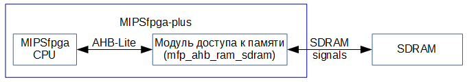
AHB-Lite Bus
It is the main tool for communicating the MIPSfpga core with the outside world. From it, the SDRAM access module receives commands for reading and writing information, and the read and write data is transmitted through it. The main feature: the phase of the address of the subsequent command coincides in time with the data phase of the current command. This is best seen in the following diagram: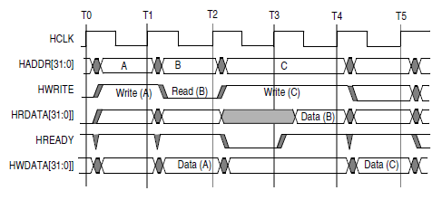
Brief description of the depicted signals: HCLK - clock signal; HADDR - the address for which we want to write or read data on the next phase is set by the master; HWRITE - at a high level, a write operation must be made in the next phase, set by the master; HRDATA - read data; HREADY - flag to complete the current operation; HWDATA - writeable data, set by the master. The bus documentation, including descriptions of all signals and their possible combinations, is included in the MIPSfpga package .
Sdram memory
The basic principles on which SDRAM is built are very well described in Chapter 5 of the Harris-Harris [1] textbook . Note the main points:
- information on the presence or absence of a capacitor charge is used to store one bit;
- memory is organized in the form of matrices of containers and control logic: with columns and rows;
- during a read operation, the charge of the cell (capacitor) is expended, after reading it has to be recharged;
- during inactivity, the amount of stored charge also decreases (albeit slower) - memory cells require periodic recharging (so-called regeneration).
We will continue further consideration on the example of Micron’s MT48LC64M8A2 chip. In addition to a very convenient and detailed datasheet, the company provides Verilog model for simulating work with this memory chip. That, on the one hand, greatly simplifies development, and on the other, it allows you, without having a debugging board, to run MIPSfpga inside the simulator and see how the kernel interacts with SDRAM.
The block diagram of the memory chip is shown in the figure below.

Main elements:
- bank (matrix) of memory (4x bank memory array) - this is where the data of interest is stored. In the considered chip, there are 4 banks, in each of which there are 8192 rows and 1024 columns of 16 bits each. Total, the total capacity of the chip 4x8192x1024x16 = 512 Mb = 64 MB.
- control device (control logic, bank control logic) - provide decoding of the received command and issuing the appropriate control signals to the other elements;
- multiplexers, latches and address bus decoders (row-address mux, 4x bank row-address latch & decoder, column-address counter / latch, column decoder) - provide storage of address information for rows, columns, and memory banks that come in different commands;
- registers and data bus logic (data output register, data input register, i / o gating, dqm mask logic) - provide input / output data for read and write operations, allow working with masks (when of 16 bits we need only the highest or lowest bytes), translate data bus pins into the Z-state, the bus is bidirectional.
Operating conditions
For the correct operation of the RAM, we need to fulfill a number of conditions. Some of them will not be considered: ensuring temperature, frequency and power stability, signal levels (static discipline), correct wiring on the board. In our field of vision remains:
- giving the correct control signals corresponding to a team;
- satisfying the requirements of dynamic discipline (Chapter 3 of the Harris-Harris textbook [1] ), taking into account the requirements of the documentation on the chip [2] .
In order to substantively understand what we are talking about, let us consider what the memory access module should do when reading data from RAM. As an example, the case of so-called. READ With Auto Precharge - when the microcircuit after the read operation itself provides recharging of the cells to which we turned. Module initialization (INIT), write operations (WRITE), or automatic regeneration (AUTO_REFRESH) are performed in the same way, with a difference in the executed commands and imposed time constraints.
Below are the copies from the datasheet: the truth table for the commands and the timing diagram, which shows how to correctly read the data.

Note: L - low level, H - high level, X - does not matter, High-Z - high impedance.
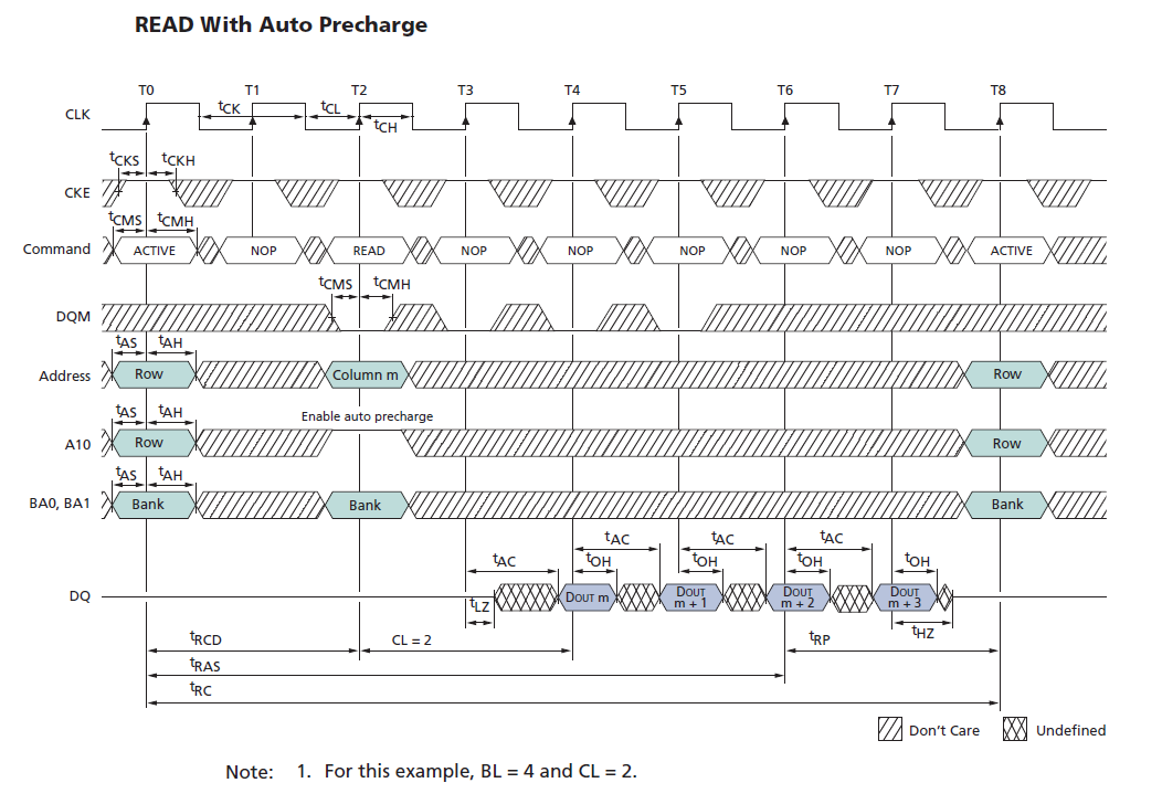
Note: tCMS - command setup time, tCMH - command hold time, tAS - address setup time, tAH - address hold time, tRCD - active command to read, tRAS - command period (ACT to PRE), tRC - command period (ACT to ACT), tLZ - output Low impedance time, tAC - access time from clock, tOH - output data hold time, tRP - commad period (PRE to ACT). The minimum values of these and other parameters for different conditions are given in the documentation for the memory chip.
Sequence of actions when reading data (in ticks)
T0. Not later than tCMS before the CLK front, ensure that there are established signals on the CS #, RAS #, CAS #, WE #, DQM pins (hereinafter referred to as the command) corresponding to the ACTIVE team. These signals should not change their state during tCMH from the time of the CLK front. Not later than tAS to the front tCLK, set the address of the line on the address bus (A [12: 0]), and the address of the memory bank on the address bus of the memory bank (BA [1: 0]). These signals must be stable for tAH after the CLK front.
T1. During (tRCD - 1 clock) to give the command NOP. After this time period has expired, the previously transmitted row address will be guaranteed saved in the row-address latch & decoder of the corresponding memory bank, one of 8192 rows will be selected (see the chip structure diagram).
T2. Not later than tCMS before the CLK front, ensure that the READ command is entered, do not change the command during tCMH since the CLK front. Not later than tAS up to the front tCLK, set the address of the column on the address bus, on the bus address of the memory bank the address of the memory bank. The tenth bit of the address bus is set to 1 as an indication that after reading you need to run Auto Precharge.
T3-T7. Ensure that the NOP command is given for the entire time the data is read and for at least (tRC - 1 clock cycle) from the time the ACTIVE command is given.
T4. After CL clock cycles (so-called CAS Latency, CAS), the read data will be guaranteed to be present on the DQ data bus. More precisely, they will appear on the bus later (1 clock + tAC) - for the case when CAS = 2. And they will be stable for at least tOH after the CLK front. During this time, the data from the bus must be read.
If you look at the interaction inside the chip, then during the time (1 clock cycle + tAC) the column address will be saved in column-address counter / latch, the output of the corresponding column memory bank will be set to signals that select the 16 bits of the column we need, this data will go to data output register and, as a result, will be on the data bus (DQ [15: 0]).
T5-T7. The example we are considering assumes that the memory chip was configured to perform batch operations (burst) with a packet size of BL = 4 (burst length, specified among other parameters by the LOAD MODE REGISTER command; in the current implementation of the memory access module, it is set as BL = 2 to get 32 bits of data). For this reason, during the next three cycles, column-address counter / latch will automatically increment by one, and another 3x16 bits will arrive at the data bus output.
It should be noted that the number of clock cycles will not necessarily be equal to 8, as shown in the diagram (T0-T7) - it must be increased in a big way in order to meet the requirements of all time constraints: tRCD, tRC, etc.
Time limit requirements are met using
- phase shift of the clock signal, on which the memory operates (CLK) relative to the clock signal on which the memory access module operates - for small intervals (tCMS, tCMH, tAS, tAH, tAC, tOH);
- giving empty commands (NOP) at large intervals (tRCD, tRC, tRP) - where the size of the delay exceeds the width of 1 clock cycle of the clock signal. To do this, the corresponding states are entered into the state machine of the module.
Clock Phase Offset
There are several good sources ( [3] and [4] ) that reasonably contrast the "scientific" approach to determining the phase shift of a clock signal to the "trial and error" method. These documents contain a number of formulas for calculating the boundaries of "safe windows", in which you need to substitute the values of delays. After that, it is proposed to shift the clock signals so that their fronts are as close as possible to the centers of these "windows". Agreeing that the described technique works, I want to draw attention to a slightly more “lazy” version of the same approach (it seems to me that it is depicted on the 12th and 20th pages of the presentation, but since there are no comments on it, I’m not sure):
- take two sheets / strips of paper into the cell (can be graph paper);
- in compliance with the scale, we apply several clock cycles to each of them, one of them - for fpga, the other - for the memory microcircuit;
- in compliance with the scale, we note on each of them:
forbidden zones in which the readable input signal should not change (A);
zones in which the value of the output signal is not defined;
zones in which the output signal is valid (B). - arrange the strips of paper in parallel and shift them relative to each other (a-la slide rule) so that the zones A are as close as possible to the centers of the zones B and in no case go beyond their boundary.
- measure the resulting clock offset with a ruler, translate it into ns according to the scale.
To ensure accurate and stable phase shift in the system, you must include a PLL module. I usually add another 3rd clock signal with a frequency 4 times higher than others and a small phase shift - in order to use it as a clock frequency for the logic analyzer (SignalTap) when debugging memory interaction in hardware.
Memory access module
This section contains the state diagram of the state machine of the memory access module, as well as individual lines of the module code describing the data reading procedure (indicating the line numbers of the code to facilitate navigation). Source code of the module as a whole: mfp_ahb_ram_sdram.v . If reading screenshots with the code gives you discomfort, fragments of the source code from the article (including comments to them) are duplicated on github .

The states of the finite state machine describing the reading procedure fully correspond to what was described above using the example of the READ With Auto Precharge diagram.

Rules for the transition between these states:
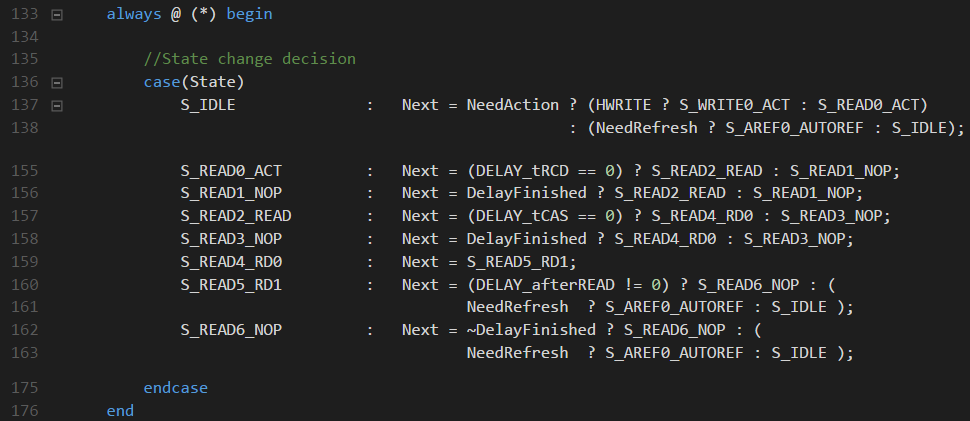
Where a delay is needed, it is entered in the delay_n register, the register's zero value corresponds to the DelayFinished flag. On the statuses S_READ4_RD0 and S_READ4_RD1, data is read from the DQ bus:
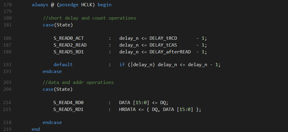
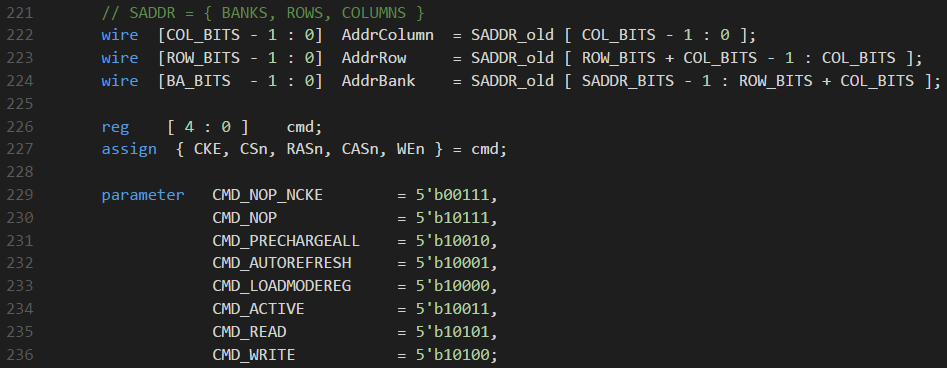
Encoding commands and their output depending on the current state:

All delays are configurable and are set in the module parameters, which should simplify porting to other cards, as well as modification of settings in case of a change in clock frequency.

Bibliography
[1] Textbook by David Harris and Sarah Harris on Digital Circuit Design and Computer Architecture
[2] Documentation on the micron memory chip MT48LC64M8A2;
[3] Quartus documentation. SDRAM controller core (translation)
[4] SDRAM PLL Tuning (presentation)
[5] Ryan Donohue. Synchronization in Digital Logic Circuits (presentation)
[6] Documentation on memory chip IS42S16320D
All datasheets, articles and presentations referenced in the article are available on github .
')
Source: https://habr.com/ru/post/321532/
All Articles