XELTEK Adapter Cloning Protection Mechanism
Foreword
This story began with the fact that we somehow needed to read / write a FLASH memory chip of the SPANSION S29GL512 type in the TSOP56 package. Until that time, we had successfully exploited the XELTEK SuperPro 500P programmer. But, unfortunately, the socket with 48 contacts installed in it did not allow this to be done even with the use of an adapter. Of course, there was no support for such chips in the program on the PC for this programmer.
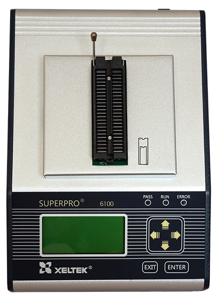
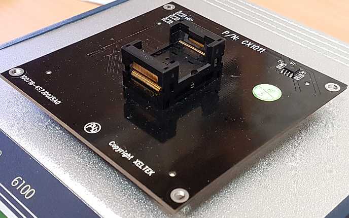
It's time to upgrade, we decided, and purchased (do not consider advertising) a programmer from the same manufacturer of the model SuperPro 6100, which uses interchangeable adapters with different sockets. Also separately purchased was the necessary, as it seemed to us then, adapter of the CX1011 model with a TSOP56 socket (an adapter with a ZIF48 socket was included with the programmer).
Let us further agree to call the programmer program simply a software, because the “programmer program” does not sound very aesthetic.
')
After receiving all this, we collected a constructor from the programmer with an adapter and tried to start working with it.
But after the required chip was selected in the software, the programmer squeaked several times and the mysterious inscription “ERROR CODE: 1D” was displayed on its display. Software also cursed the message that this adapter is not suitable for programming this chip. How so!? The adapter with the programmer got married happily, the chip with the socket too, but the malicious manufacturer decided that this is not enough and the user, in addition to the new programmer, must also purchase the “new” adapter DX1011. For which, by the way, on the manufacturer's website they want about three hundred evergreens. Well, okay, in our case, we bought it by mistake, although there was still no desire to acquire a “new” one. But after all, someone could save it from the old programmer, and someone might want to make it yourself. So for this particular audience this article.
In preparing this material, we did not set out to teach the reader to use various programs and hardware devices that had to be used along the way. Therefore, we will not clutter the article with a description of the subtleties of working with all these tools, leaving it behind the scenes. But if someone is interested in the details, we will be happy to comment on them.
Here it’s just right to cite the text of the disclaimer about liability, the meaning of which is that the author is not responsible for any use you make of the materials in this article. In other words, only you yourself will be responsible for your actions, to which you may be encouraged to become familiar with this material.
Exploratory survey
An overview of the adapter made it possible to detect on it an octopus microcircuit labeled AE801, of which there was, of course, no documentation on the Internet. This microcircuit is clearly visible in the right corner in the photo of the CX1011 adapter above.
Although some information about this chip is still found. The XELTEK website in the FAQ section answers the question: “What is the difference between the SuperPro 6000 and 6100 programmers?” There is a curious phrase: “The CX series adapters (for 6000 programmers) and DX (for 6100 programmers) are absolutely the same, except for the ID chip, which in adapters of the DX series uses advanced protection. ”It became clear that this chip is a kind of ID chip that the programmer uses to identify the adapter installed in it. That's just what kind of protection is it: from whom or from what does the adapter need to be protected? Well, of course from us with you!
This protection is similar to the one that is now commonly used in printer cartridges so that they are not refilled and bought new ones. But here the situation is somewhat different. You get an expensive adapter for your money and hope that you will use it forever. Not here it was! The manufacturer of this prudently took care of and, having become like the Creator himself, decided to artificially limit the adapter to the period of his mortal life. In confirmation of this, the following significant messages are found in the software:
- “Socket adapter end-of-life is near. Please prepare to replace with a new one. "
“Adapter usage beyond its cycle life, please change.”
How do you like this pearl: “Adapter life expires”? And especially the phrase "replace with a new one", so caressing the ear of the sales department.
For some reason, on the XELTEK website on the page with adapters about their perishability - not a word! Paraphrasing one famous saying about a goat and a button accordion, I just want to say: “What about protection adapter?”
But be that as it may, the need to still read / write a FLASH memory chip (which, I must say, we have forgotten, carried away by everything else) and an irresistible desire to by all means alleviate the plight of the unfortunate The adapter made us move on.
Preparation for treatment
We will further agree to call the PC on which the software for the programmer is running as the host.
For data exchange between the host and the programmer uses a USB interface, and in it several USB channels (Pipes). The host sends commands to the programmer via one of the USB channels, sends data to it via the other, and receives data from the programmer through the next.
It was necessary to identify the interface for data exchange between the AE801 and the programmer itself. Here the manufacturer did not philosophize, using the good old UART with a speed of about 10,500 baud. The AE801 chip, which is essentially an eight-legged microcontroller, legs 1 and 4 are connected to ground, + 5V is powered to foot 8, foot 3 is used for bidirectional data transfer via UART, foot 7 is used as positive CS, and to foot 6, simultaneously with the appearance of the unit on the leg 7, the clock frequency is 4 MHz. Of the eight legs that we know of microcontrollers, ATMEL of ATtiny25, 45, 85 series is best suited for this pinout. However, the SOIC8 package used for them is somewhat wider than necessary.
When studying the data exchange between the AE801 on the adapter and the programmer, one interesting thing was discovered: when choosing a chip in the software, even before the AE801 chip is selected on the adapter, some data packets appear on its leg 3. It turned out that there is even before the start of communication with the chip from the adapter, the programmer communicates with someone else. Later it turned out that the programmer itself has the same AE801 chip, sitting on the same bi-directional data bus as the AE801 from the adapter. And it serves the same purpose - protection from cloning, but now the programmer itself.
Further, the software on the host was modified to save the data exchange procedure between it and the programmer to a log file. From the received log it became absolutely clear that nothing is clear. The data exchange was somehow encrypted and noisy with garbage. Apparently that was precisely the “improvement of protection”. But one thing became obvious - the adapter informs the programmer of the name of its model, directly in text form, and its age, so that it can be sent in a timely manner to a well-deserved, in the opinion of XELTEK, rest. Everything else is rubbish.
By further study, it turned out that the protection algorithm was written by a person very far from this topic. The so-called "enhanced protection" does not hold water.
However, it was not possible to figure out the log in the forehead and it became obvious that now it is necessary to move inside the programmer itself. Its electronic filling looks like a layer cake, in the form of a set of individual boards, connected together with racks and connectors.

One of these boards (let's call it, by analogy with a PC, “motherboard”) contains an ARM microcontroller ATMEL AT91SAM9G20, SDRAM, SPI FLASH with firmware, the same AE801 ID chip with a programmer model and its serial number, a USB controller chip, and a number of other chips .
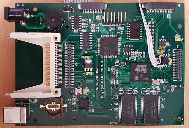
Another XILINX microcircuit is installed on one motherboard, which, together with the other motherboards with transistor assemblies, controls the legs of the microcircuit on the adapter connected to the programmer during read / write procedures, etc.

The entire ARM microcontroller firmware is contained in the external SPI FLASH chip, which, of course, also does not contribute to the increased protection. Usually, the bootloader is hidden in the internal memory of the microcontroller, which is inaccessible for reading, and the firmware or updates placed outside are encrypted. But the developers of XELTEK decided to go the other way, confusing themselves with proprietary AE801 chips, leaving the ARM firmware to be torn apart. What we actually do next.
The idea was to disassemble the “usb” file of the programmer's algorithm and then assemble the project in one of the ARM IDE, so that later through JTAG, having source code in assembler, study the work of the programmer in terms of his communication with the AE801 chip.
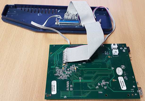
On the motherboard, a place for the JTAG connector was provided by the way. For easy debugging, the JTAG connector was mounted on the side of the plastic housing of the programmer and connected to the motherboard with a flat cable.
The result was a kind of Development Kit.
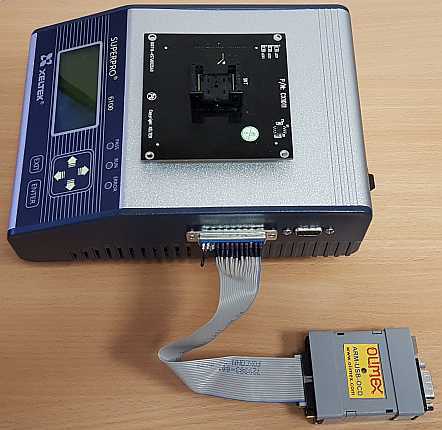
Since we had JTAG OLIMEX ARM-USB-OCD, preserved from some old project, the choice of ARM IDE fell on the IAR Embedded Workbench, because it supports debugging through the GDB server. However, setting up this very GDB server turned out to be a very intricate task. And it was necessary to spend some time to get the project assembled from the assembler source code into the SDRAM programmer and the opportunity to debug it.
After everything finally worked out from under the debugger, some of the most "interesting" methods of the algorithm were rewritten to C to make them easier to understand. Thus, gradually managed to accumulate information, which allowed to understand the mechanism of the programmer, which is described below in a somewhat simplified form.
When the programmer is powered on, its built-in bootloader (conditionally zero) starts up in the ARM microcontroller, loads another bootloader from SPI FLASH (let's call it first) into its internal RAM, remaps this RAM to address 0 and transfers control to the first bootloader. Having started work, the first loader sets up the controller in ARM-e SDRAM, thus connecting the external RAM at 0x20000000 and rewrites another bootloader (let's call it second) from the same SPI FLASH and transfers control to it. The second loader configures the external USB controller chip to communicate with the host, displays the screen with the name of the programmer and the firmware version on the LCD, communicates with its own ID chip AE801 and eventually enters the command processing loop from the host.
To work with each type of memory chips created its own firmware for ARM microcontroller, called the algorithm. Algorithm files have the “usb” extension and are stored on the host in the “algoX” directory with the installed program. The “lib” directory contains firmware for the XILINX chip and files with the “wls” extension, which contain information on the correspondence of the required algorithm to each chip supported by the programmer, the type of adapter required for this chip, as well as some additional parameters for each chip. For example, its supply voltage, programming voltage, etc.
After choosing a chip in the software, you need to make sure that the corresponding adapter is installed in the programmer. For this, the host sends a command to the programmer — a request of the type of adapter installed in it. The programmer asks the AE801 chip from the adapter for its type and sends the generated response in a special way back to the host. The software on the host compares the adapter type from the “wls” file with the adapter type from the response and, if they match, sends the next bootloader (let's call it the third) to the programmer at 0x20020000 - the “loader.bin” file located in the “bin” directory. After transferring control to the third loader, the host with its help loads the algorithm (usb file) corresponding to this type of chip to the address 0x20000000, the firmware for XILINX and eventually transfers control to the loaded algorithm. After some adjustments of the hardware, the algorithm, in turn, again falls into the loop of processing commands from the host. The intermediate third loader is needed only so that the working algorithm is loaded each time at the same address 0x20000000.
When you select another chip in the software, the entire procedure described above is repeated, starting with a request from the host for the type of adapter installed in the programmer.
After the algorithm loaded into the programmer enters the loop of processing commands from the host, all further actions are activated only by these commands. In other words, the host becomes the master, and the programmer the slave. The AE801 microcircuit from the adapter is slave with respect to the programmer and, after feeding on its leg 7 (CS), an active high level, and for the leg 6 clock frequency 4 MHz also goes into the command processing cycle from the programmer. Leg 3 of the AE801 chip is initially configured to receive commands from the programmer. After sending the next command, the programmer sets up the data line for reception, and the AE801, respectively, its leg 3 for transmission and sends the data to the programmer. Thus, data is exchanged between the AE801 in the adapter and the programmer. Data is exchanged between the internal AE801 on the motherboard and the programmer in exactly the same way.
Treatment
So, we came directly to the consideration of the mechanism of protection adapters DX series.
As mentioned earlier, in order not to overload the article with unnecessary details, here we give only the quintessence of the path covered - a description of the process of data exchange between the programmer and the AE801 ID chip.
Terminology used in this description:
- The term “leg” refers to the corresponding pins of the AE801 chip.
- Byte counting - starting from one.
- Each time, the programmer, sending a certain number of bytes to the microcircuit, transfers the data line to the reception, and the microcircuit, having received this data, switches leg 3 to the transmission, etc. Therefore, the description of these switches and the mention of the legs 3 will not be given.
- The narration is on behalf of the chip AE801.
1. If there is an inactive low level on leg 7, leg 3 is set to enter and we are either in a reset or in a state of sleep.
2. When the programmer gives active high level to leg 7 (leg 6 of 4 MHz is supplied to leg 6), we have to transfer 6 random bytes to the programmer.
It is known that to use the algorithm for generating random, or rather, pseudo-random numbers from the standard library C, you must first call the srand () command, passing a certain number, a salt, as the input argument, using which each call to the rand () command will return the following value from defined by this number of pseudo-random sequence. In PC, time () is usually used as a source of entropy for srand (), but in simple microcontrollers, as a rule, there is no real time clock and this task can be solved, for example, by saving a new value for srand () in the EEPROM each time after reset. Most likely, this is how it was implemented in AE801. By and large, we don’t need to generate random numbers at all, but the solution to this problem seemed interesting.
We implemented the AE801 prototype on a Microchip microcontroller (at that moment it was just at hand), which operated from its own internal generator at a frequency of 8 Mhz and with respect to it an external frequency of 4 MHz, fed to leg 6, turned out to be acceptable (and perhaps the only) source of entropy.
Leg 6 in the program was used as a digital input and 16 bits were read from it in the cycle, which are necessary for transmission to the srand () method.
3. We receive from the programmer 9 bytes and confirm their receipt by sending to the programmer the sixth byte received.
4. We receive from the programmer 5 bytes. The first of five received bytes is sent to the programmer as is, and the remaining 4th ones are encrypted using the RSA algorithm in 4th 16-bit words and sends the received 8 bytes to the programmer. Moreover, for each of the words received after encryption, the high byte is sent first, and then the low byte. Finally, we send the first five received bytes to the programmer again. Total 10 bytes.
RSA with very short keys 63, 847 and 2773 is used as an encryption algorithm. Anyone interested can find information about this, for example, HERE .
In the firmware of the algorithm, the cycle of 2773 iterations is used to calculate RSA. But since the input number for encryption is a byte, and the output is a two-byte word, to simplify the calculation of RSA, a table of 256 words was formed, which took an extra 512 bytes of program memory.
RSA table
{ 0x0000, 0x0001, 0x03d0, 0x0640, 0x059d, 0x045f, 0x0191, 0x020b, 0x0863, 0x0209, 0x0933, 0x0489, 0x017f, 0x0168, 0x00d8, 0x0717, 0x0741, 0x0315, 0x040d, 0x0368, 0x0984, 0x084f, 0x06d8, 0x0832, 0x08b2, 0x0602, 0x07aa, 0x06a4, 0x0044, 0x086f, 0x08da, 0x07cd, 0x067f, 0x099f, 0x0797, 0x0086, 0x0ab4, 0x0088, 0x09e6, 0x07c5, 0x0433, 0x082a, 0x06d4, 0x00d0, 0x06f8, 0x029d, 0x0496, 0x04f5, 0x0525, 0x06ef, 0x037f, 0x02ad, 0x0606, 0x0133, 0x03b2, 0x0573, 0x0a1d, 0x017d, 0x09ad, 0x0674, 0x05ff, 0x0745, 0x097a, 0x02d9, 0x0373, 0x02f3, 0x09a6, 0x0402, 0x0969, 0x05be, 0x01c5, 0x0ab7, 0x042c, 0x074c, 0x0965, 0x047d, 0x0989, 0x0a81, 0x00a4, 0x00fd, 0x03ee, 0x099c, 0x0695, 0x05ee, 0x028d, 0x0435, 0x0243, 0x07df, 0x09d1, 0x07ee, 0x0509, 0x09b9, 0x023f, 0x02c0, 0x06fa, 0x098d, 0x05d5, 0x0499, 0x0800, 0x016f, 0x0019, 0x0410, 0x010b, 0x01ab, 0x07ea, 0x036f, 0x0094, 0x004e, 0x0a64, 0x06b9, 0x0abe, 0x051a, 0x0295, 0x0078, 0x0112, 0x06a8, 0x08dd, 0x06e9, 0x04d7, 0x08c3, 0x02e4, 0x00f3, 0x0015, 0x09e7, 0x0967, 0x06e2, 0x0650, 0x0508, 0x0882, 0x0028, 0x07f3, 0x00b7, 0x03d7, 0x0504, 0x0143, 0x0016, 0x0995, 0x08b5, 0x0437, 0x0763, 0x04c5, 0x0234, 0x04c7, 0x07da, 0x09bd, 0x027e, 0x051b, 0x01c0, 0x052a, 0x0544, 0x046c, 0x078c, 0x0199, 0x0299, 0x04b6, 0x094a, 0x07d3, 0x053c, 0x0083, 0x017b, 0x00d6, 0x077f, 0x090b, 0x0475, 0x00ab, 0x09cc, 0x0312, 0x0603, 0x0907, 0x07fa, 0x00b9, 0x0909, 0x0889, 0x0360, 0x0247, 0x00cc, 0x054c, 0x0213, 0x054e, 0x0a44, 0x0767, 0x07b0, 0x0074, 0x087b, 0x041e, 0x098a, 0x087d, 0x03ab, 0x069c, 0x06cc, 0x0604, 0x095f, 0x053f, 0x0954, 0x02da, 0x06d1, 0x08f0, 0x09bf, 0x01db, 0x039e, 0x08a8, 0x0ac5, 0x007a, 0x0222, 0x0a8f, 0x042f, 0x0322, 0x01f0, 0x00e3, 0x00f7, 0x0417, 0x09aa, 0x00fc, 0x077a, 0x04e9, 0x0a21, 0x0278, 0x06f7, 0x07ef, 0x08e7, 0x09cd, 0x04aa, 0x0739, 0x09e3, 0x0708, 0x0a72, 0x028e, 0x04a6, 0x04c0, 0x021b, 0x081d, 0x05c5, 0x069a, 0x05bc, 0x06ca, 0x00eb, 0x00ec, 0x0a9b, 0x04f7, 0x07a2, 0x04ec, 0x0338, 0x05b7, 0x0459, 0x043d, 0x02f5, 0x0284, 0x023b, 0x01f5, 0x0979, 0x01c4, 0x027b, 0x0868, 0x043c, 0x0397, 0x048f }; 5. We get from the programmer 1 byte and remember it as a marker. After that we send random 4th bytes to the programmer. The programmer, having received these 4 bytes, in the same way as we in paragraph 4 encrypts them using the same RSA algorithm and sends us the resulting 8 bytes in the same order (first the highest, then the low byte from each word). Having received these 8 bytes, we have to check whether the programmer has coped with the task and, if the answer is positive, we send him the previously received marker.
6. We receive from the programmer 1 byte and again we remember it as a marker. Then we form in the array, say, buf11 - 11 random bytes and save it for subsequent actions. Then, in a sly way, we send these 11 bytes to the programmer. The trick is that we have to send 88 bytes to the programmer, into which the 11 formed by us will be packed, and the low bit of the marker is used to invert the transmitted 11 bytes. After sending 88 bytes to the programmer, we send the received marker to it.
Litter Code in C.
byte _mark; // . byte _buf11[11]; // 11- . for( i=0; i<11; i++ ) { byte bt = rand(); _buf11[i] = bt; if( _mark & 1 ) bt = ~bt; // 8. // for( j=0; j<8; j++ ) { byte rnd = rand(); byte msk = ( 1 << j ); if( bt & msk ) rnd |= msk; else rnd &= ~msk; // rnd . // ( rnd ); } } // . // ( _mark ); 7. We receive from the programmer 1 byte and send to it an array of 133 bytes, consisting of four parts.
The first part - 48 bytes with information about the type of adapter and its "age" was taken from the native adapter "DX0001", in which the text "DX0001" was replaced by "DX1011".
Adapter id
{ 'D', 'X', '1', '0', '1', '1', 0xff, 0xff, 0xff, 0xff, '1', '6', '0', '6', '2', '4', 0xff, 0xff, 0xff, 0xff, 0xff, 0xff, 0xff, 0xff, 0xff, 0xff, 0xff, 0xff, 0xff, 0xff, 0xff, 0xff, 0x50, 0x00, 0xff, 0xff, 0x00, 0x00, 0x0c, 0xff, 0xff, 0xff, 0xff, 0xff, 0xff, 0xff, 0xff, 0xff }; The second part is 16 random bytes.
The third part is 22 bytes, specially formed from the previously saved buf11 11 bytes.
The code for the formation of 22 bytes in C
byte _buf22[22]; const byte _hash[] = { 0x58,0x3E,0x09,0x2D,0xFD,0x45,0x68,0x10,0xD5,0x25,0xC7,0xB8,0x28,0x93,0x75,0xDE, 0x57,0x02,0x1E,0x24,0x36,0xB6,0x3A,0x59,0x11,0x6E,0x58,0x91,0xAE,0x53,0x69,0xDF, 0x44,0xA4,0x8B,0xFB,0x76,0x91,0x59,0x3C,0x30,0xB9,0xDA,0x21,0xD8,0x05,0xB4,0x16, 0x4C,0x05,0x78,0x8D,0xB5,0x1C,0x41,0x63,0x4C,0xBE,0xA6,0xCC,0x65,0xB8,0x38,0x1D, 0xE7,0xC6,0xC9,0x19,0xB7,0x73,0xB2,0x7D,0xCD,0x54,0xDC,0xFE,0x67,0x5E,0x79,0x68, 0xB8,0x77,0x73,0x37,0xC8,0x56,0xA2,0x4D,0x9B,0x86,0x56,0x3F,0x26,0x39,0xDE,0xF6, 0xA8,0x13,0xB4,0xBA,0x19,0xDE,0xDF,0x08,0x64,0x2A,0x9F,0xA4,0x3E,0xEE,0x90,0x5B, 0xF0,0xF3,0xC6,0x5F,0x1F,0x84,0x87,0xA3,0x94,0x0D,0x04,0x92,0xDC,0x3C,0xD0,0x6A, 0xD6,0x9B,0xA9,0xED,0x02,0xB0,0xB3,0xBB,0xF3,0x17,0x04,0x93,0x8F,0x18,0x22,0x9B, 0x33,0x0F,0x2A,0x4C,0x72,0x1A,0x0F,0xC2,0x3E,0x4C,0x77,0xAA,0xF2,0x04,0xDC,0x60, 0x68,0x81,0x7B,0x7C,0x60,0xE7,0xD3,0x61,0x3A,0xDA,0x69,0x4A,0x14,0x5A,0xB7,0x31, 0x9F,0xB5,0x60,0x61,0xB4,0x2D,0x80,0x10,0xCF,0x16,0x6B,0xF1,0x08,0x81,0xDA,0x12, 0xA6,0x46,0xF2,0xA2,0x14,0x68,0xAA,0x48,0x94,0x8B,0x9D,0xE3,0xD0,0xFB,0x84,0x74, 0x1C,0x3C,0x94,0x5A,0x3F,0xF0,0x37,0x8C,0xD9,0x7E,0xA7,0x38,0xA4,0xB5,0xA7,0x25, 0x65,0x15,0x7F,0xE5,0x3B,0xD1,0x14,0x1E,0xD3,0xA8,0x47,0x2E,0xD8,0xEB,0xB0,0xAE, 0x4F,0x34,0xF4,0x52,0xC7,0x23,0x9D,0x60,0x98,0x1E,0x2C,0xFC,0xF2,0x96,0xB7,0x83 }; void PrepareBuf22() { byte i, j, bt, bt1, bt2, bt3; for( i=0; i<4; i++ ) _buf22[i] = rand(); bt2 = (_buf22[1] ^ _buf22[2] ) & 0xEF; bt3 = _buf22[1] ^ _buf22[3]; _buf22[4] = (byte)((_buf22[0] + _buf22[1] + _buf22[2]) ^ _buf22[3]); _buf22[1] ^= ( 1 << (_buf22[2] & 7) ); bt = _buf22[2]; bt1 = _buf22[0]; i = 0; while( i < 10 ) { bt += _buf11[i++]; bt1 += _buf11[i++]; } _buf22[5] = bt; _buf22[6] = bt1; // ---------------------------------------------------------------- _buf22[7+11] = 0; _buf22[7+12] = 0; for( i=0; i<10; i++ ) { _buf22[7+11] += _buf11[i]; _buf22[7+12] ^= _buf11[i]; } _buf22[7+11] ^= _buf11[9]; _buf22[7+12] ^= _buf11[10]; _buf22[7+13] = (_buf22[7+11] + _buf11[10]) ^ _buf22[7+12]; _buf22[7+14] = (_buf22[7+13] + _buf11[9]) ^ _buf22[7+12]; for( i=0; i<15; i++ ) { bt = (_buf22[7+i] ^ _hash[bt2+i] ); bt = (bt << 2) | (bt >> 6); bt ^= bt3; _buf22[7+i] = bt; } } The fourth part - 47 random bytes.
8. After transmitting an array of 133 bytes, the microchip should either go to sleep until the next active high level appears on pin 7, or it automatically switches to the reset state, in case pin 7 is a reset signal. And then everything repeats, starting with paragraph 2.
Extract recovered patient
In the end, the CX1011 adapter was safely put on its feet and got a second life in a new programmer.
Hopefully, the material in this article will help readers safely revitalize other “old” adapters, and perhaps make their own.
Source: https://habr.com/ru/post/320870/
All Articles