Connect Xmega to FRAM over SPI
In one of the devices, it became necessary to fully restore the previous mode of operation in the event of any power failure or short-term shutdown. It was certainly possible to lay a backup power source, but its use was limited, so to speak, by the design features of the device. As a result, it was decided to record a series of values necessary for restoring to memory. Since I was going to update the values for recovery often, due to the limited number of write cycles, the use of Flash and EEPROM was not even considered.
In my opinion, at the moment the most optimal solution for such cases is the FRAM memory. It would be possible to write the necessary data cyclically to Flash, constantly incrementing the address for new values, but in this case it was necessary to save the pointer somewhere to the latest values, or read Flash completely and then retrieve the “latest” data.
The Lapis Semiconductor has three lines of FRAM chips that communicate with the master via I2C or SPI, or via a parallel interface. The advantages of serial interfaces over parallel ones are obvious. As for I2C and SPI, the data transfer rate for SPI is 4 times higher than for I2C, but the consumption in this connection is almost 16 times higher.
')
I didn’t have to choose, there was only MR45V256 with 32 KB of memory and SPI interface. 32 KB for my needs is more than enough, so I used the remaining memory to record all sorts of technical information and log commands received from the operator.
Working with FRAM memory is very simple. Any operation begins with the transfer of the selection line of the slave device CS # to a low state. Then one of the operations teams is sent, there are only 6 of them:
- Read data (READ)
- Data Recording (WRITE)
- Entry in the FRAM status register (WRSR)
- Reading FRAM Status Register (RDSR)
- Setting Data Overwrite Protection (WRDI)
- Remove data protection from overwriting (WREN)
Overwrite protection can be installed either on the first quarter of the memory, on the first half, or on the entire memory. In cases with read and write commands, after them you must also send a hexadecimal address from which reading / writing will begin. The command and address are sent one-time, later the microchip itself increments the address and transmits all subsequent data until CS # is set to high.
Before you start writing to memory, you must always set the write enable bit (WREN) in the status register MR45V256. And only after that transfer the write command (WRITE).
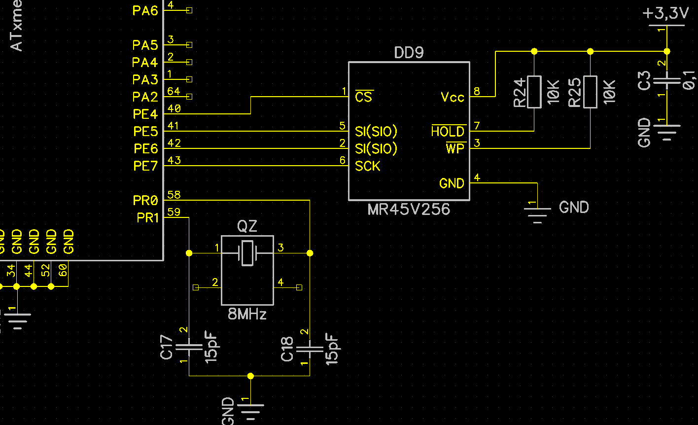
As the master device used a microcontroller Xmega. Xmega's SPI microcontrollers are almost identical to those of other Atmel microcontrollers. The most noticeable difference is the possibility of using DMA, but in this case I do not have large amounts of transmitted information, so I refused to use DMA. Xmega supports all 4 SPI modes of operation (Mode 0,1,2,3). It is worth noting that the MR45V256 only supports Mode 0 and Mode 3.
The SPI module in Xmega is equipped with single-level buffering in the transmission channel and two-level buffering in the receiving channel. That is, the bytes to transmit cannot be placed in the SPI data register until the shift cycle is fully completed. During the reception of data, the received parcel must be read before the reception of the next parcel is completed. Otherwise, the first data byte will be lost. Therefore, it is recommended to work either on interrupts, or when receiving and transmitting, to monitor the SPI status register.
There are no commands for erasing in FRAM, since data can be overwritten without first erasing, as for example in other types of memory. However, sometimes it is necessary to completely “erase” the entire FRAM:
If we talk about the benefits of using FRAM, then first of all it is reliability. The number of write cycles is 10 to 12 degrees. The manufacturer promises up to 10 years of information storage without losing it. Compared to the same FLASH, the FRAM memory has a high speed and much lower consumption. Of the minuses can be noted if only not a large amount of memory, but given the tasks for which usually use FRAM, large amounts are not so important.
In my opinion, at the moment the most optimal solution for such cases is the FRAM memory. It would be possible to write the necessary data cyclically to Flash, constantly incrementing the address for new values, but in this case it was necessary to save the pointer somewhere to the latest values, or read Flash completely and then retrieve the “latest” data.
The Lapis Semiconductor has three lines of FRAM chips that communicate with the master via I2C or SPI, or via a parallel interface. The advantages of serial interfaces over parallel ones are obvious. As for I2C and SPI, the data transfer rate for SPI is 4 times higher than for I2C, but the consumption in this connection is almost 16 times higher.
')
I didn’t have to choose, there was only MR45V256 with 32 KB of memory and SPI interface. 32 KB for my needs is more than enough, so I used the remaining memory to record all sorts of technical information and log commands received from the operator.
Working with FRAM memory is very simple. Any operation begins with the transfer of the selection line of the slave device CS # to a low state. Then one of the operations teams is sent, there are only 6 of them:
- Read data (READ)
- Data Recording (WRITE)
- Entry in the FRAM status register (WRSR)
- Reading FRAM Status Register (RDSR)
- Setting Data Overwrite Protection (WRDI)
- Remove data protection from overwriting (WREN)
Overwrite protection can be installed either on the first quarter of the memory, on the first half, or on the entire memory. In cases with read and write commands, after them you must also send a hexadecimal address from which reading / writing will begin. The command and address are sent one-time, later the microchip itself increments the address and transmits all subsequent data until CS # is set to high.
Before you start writing to memory, you must always set the write enable bit (WREN) in the status register MR45V256. And only after that transfer the write command (WRITE).
As the master device used a microcontroller Xmega. Xmega's SPI microcontrollers are almost identical to those of other Atmel microcontrollers. The most noticeable difference is the possibility of using DMA, but in this case I do not have large amounts of transmitted information, so I refused to use DMA. Xmega supports all 4 SPI modes of operation (Mode 0,1,2,3). It is worth noting that the MR45V256 only supports Mode 0 and Mode 3.
The SPI module in Xmega is equipped with single-level buffering in the transmission channel and two-level buffering in the receiving channel. That is, the bytes to transmit cannot be placed in the SPI data register until the shift cycle is fully completed. During the reception of data, the received parcel must be read before the reception of the next parcel is completed. Otherwise, the first data byte will be lost. Therefore, it is recommended to work either on interrupts, or when receiving and transmitting, to monitor the SPI status register.
// SPIE #define FRAMPORT PORTE // FRAM PORT #define SPIRESET 0 #define SPICS 4 #define SPIMOSI 5 #define SPIMISO 6 #define SPISCK 7 // SPIE(FRAM) void SPIE_init() { FRAMPORT.DIRCLR = (1<<SPIMISO); // SPI FRAMPORT.DIRSET = (1<<SPIMOSI) | (1<<SPISCK) | (1<<SPICS); // SPI FRAMPORT.OUTSET = (1<<SPICS); // SPI , , SPI Mode 0, 4 SPIE.CTRL = SPI_ENABLE_bm | SPI_MASTER_bm | SPI_MODE_0_gc | SPI_PRESCALER_DIV4_gc; } // FRAM void FRAM_WREN() { SPIE_init(); FRAMPORT.OUTCLR = (1<<SPICS); // ChipSelect SPIE.DATA = 0x06; // while( !(SPIE_STATUS & SPI_IF_bm) ); // FRAMPORT.OUTSET = (1<<SPICS); // ChipSelect PORTE.OUTCLR = (1<<SPICS); // ChipSelect SPIE.DATA = 0x02; // while( !(SPIE_STATUS & SPI_IF_bm) ); SPIE.DATA = 0x00; // while( !(SPIE_STATUS & SPI_IF_bm) ); SPIE.DATA = 0x10; // while( !(SPIE_STATUS & SPI_IF_bm) ); SPIE.DATA = Data1; // while( !(SPIE_STATUS & SPI_IF_bm) ); SPIE.DATA = Data2; while( !(SPIE_STATUS & SPI_IF_bm) ); SPIE.DATA = Data3; while( !(SPIE_STATUS & SPI_IF_bm) ); FRAMPORT.OUTSET = (1<<SPICS); // ChipSelect SPIE.CTRL = 0x00; FRAMPORT.OUTCLR = (1<<SPIMOSI) | (1<<SPISCK); } // FRAM void FRAM_RD() { SPIE_init(); FRAMPORT.OUTCLR = (1<<SPICS); // ChipSelect SPIE.DATA = 0x03; while( !(SPIE_STATUS & SPI_IF_bm) ); SPIE.DATA = 0x00; // while( !(SPIE_STATUS & SPI_IF_bm) ); SPIE.DATA = 0x10; // while( !(SPIE_STATUS & SPI_IF_bm) ); SPIE.DATA = 0x00; // while( !(SPIE_STATUS & SPI_IF_bm) ); Data1 = SPIE.DATA; SPIE.DATA = 0x00; while( !(SPIE_STATUS & SPI_IF_bm) ); Data2 = SPIE.DATA; SPIE.DATA = 0x00; while( !(SPIE_STATUS & SPI_IF_bm) ); Data3 = SPIE.DATA; FRAMPORT.OUTSET = (1<<SPICS); // ChipSelect SPIE.CTRL = 0x00; FRAMPORT.OUTCLR = (1<<SPIMOSI) | (1<<SPISCK); // SPI } There are no commands for erasing in FRAM, since data can be overwritten without first erasing, as for example in other types of memory. However, sometimes it is necessary to completely “erase” the entire FRAM:
void FramErase(void) { SPIE_init(); FRAMPORT.OUTCLR = (1<<SPICS); // ChipSelect SPIE.DATA = 0x06; // WREN while( !(SPIE_STATUS & SPI_IF_bm) ); // FRAMPORT.OUTSET = (1<<SPICS); // ChipSelect PORTE.OUTCLR = (1<<SPICS); // ChipSelect SPIE.DATA = 0x02; // while( !(SPIE_STATUS & SPI_IF_bm) ); SPIE.DATA = 0x00; // while( !(SPIE_STATUS & SPI_IF_bm) ); SPIE.DATA = 0x00; // while( !(SPIE_STATUS & SPI_IF_bm) ); while(FramCounter <= 0x7FFF) { SPIE.DATA = 0x00; while( !(SPIE_STATUS & SPI_IF_bm) ); FramCounter++; } FRAMPORT.OUTSET = (1<<SPICS); // ChipSelect FramCounter = 0; SPIE.CTRL = 0x00; // SPI FRAMPORT.OUTCLR = (1<<SPIMOSI) | (1<<SPISCK); } If we talk about the benefits of using FRAM, then first of all it is reliability. The number of write cycles is 10 to 12 degrees. The manufacturer promises up to 10 years of information storage without losing it. Compared to the same FLASH, the FRAM memory has a high speed and much lower consumption. Of the minuses can be noted if only not a large amount of memory, but given the tasks for which usually use FRAM, large amounts are not so important.
Source: https://habr.com/ru/post/320472/
All Articles