Electronics development: from idea to device

Now it is much easier to find funding for your project, start-up alleys are held, crowdfunding platforms are full of novelties. Arduino brought the dreamers closer to their cherished fame. IoT technologies took their toll and IT firms realized that it’s not possible to live by one code. It is not uncommon when the hardware project is managed by people who are somewhat far from electronics. And even more often they think that the life cycle of a software project is similar to the life cycle of a hardware project. Alas, it is not.
The organization of the process of developing iron is a very important moment. Error at any stage can "get out sideways" and the price can be prohibitively high. When creating a material object, it is not possible to release a new version every day. Designing is the most difficult development stage and we will talk about it later.
Note 1: this material is intended for people who are not familiar with (real) development, these are students and teachers, startups, IT firms, programmers. All of the above - personal experience and observation. If you are an engineer with experience and you have something to add - write in the comments.
')
Note 2: here we are talking about a simple life cycle, from the idea to the piece of hardware, but not to the sale. Why is that? Projects of varying complexity can go through many stages before the sale: searching for an investor, if not, legal red tape, mockup, layout, device, debugging, development of debugging stands (which can be even more complicated), certification, serial device.
PP - printed circuit board;
TZ - technical task;
BOM - Bill Of Materials or the list of elements.
Project life cycle

- Preparation of TK (general concept, functions, elaboration of potential solutions, comparison with the terms);
- Development of an approximate concept (pictures for bosses / sponsors);
- Drawing up a Gantt chart / timetables / deadlines;
- Statements of tasks with the team;
- Development of software + writing a program for MC;
- Drawing of the case (according to the approved 3D model) + order of PP and purchase of components for PP;
- Installation of software + production of the case;
- Debugging, a lot of debugging, sea debugging;
- Testing;
- Fotochki / press releases / tears / calls mom.
Team
A good team is an integral part of the project. Since we have to work with different people and join projects at different stages, the actual “hardware project life cycle” was then described. There are various specialists in electronics: a circuit engineer, a PCB engineer, a software engineer (low level, i.e. microcontrollers, microprocessors, FPGAs), a process engineer, technical designer, installer and technical manager or technical director. There is such a category as Embedder is an expert who calculates the scheme, designs, programs, solders (and the Swiss, and the reaper, and the dudo player). There is often an opinion among customers that you need to hire a person who will do everything, but the division of labor is the best position and you should not blame everything on one person, especially when it comes to a startup when you need to fit into a tight time frame and do a lot of work.
// Naturally, they started arguing with a colleague about this. They say that startups don't have a lot of money, but, in my opinion, the amount of money is already a concern not of an engineer or of those directors. If you want one person, he will have to work day and night, and you have to pay very well for this (it is cheaper to take assistants to him), besides, such work may be interesting for some time, but then burnout may simply begin. The specialist throws everything and goes into the sunset, while the authorities burn and burn.

Not so long ago, I was asked how all the same formed a team for a project of varying complexity. Actually it depends on a lot of factors: timeframes, financial constraints, initial data (for example, previous developments), what you need to get at the output (dummy, layout, beautiful layout, device, serial version, etc) and from the lead project. For a simple project, such as a driver for a certain LED thing, one of them can be enough (calculated the scheme, distributed it, soldered it, programmed it in production). There was a medical project with the following: a presenter, an embeder for the main unit and an energy transfer unit, a low-level programmer for working with information transfer, a high-level programmer (software for PC and phone), near-engineer for small work (for that far moment I) type of drawing library components for CAD, documentation, theor. calculations, a separate logistic (he himself was engaged in procurement and control of supplies), technologist and technical designer. But this is taking into account the fact that there were previous versions of the device, the specialists who developed them, deadlines moved many times, debugging and testing on living samples (no one was hurt). There was a lot of work, but at the initial stage no one presented HOW MUCH a lot, although there was some groundwork and experience.
For the project of wearable devices, I have enough designer PP, who is engaged in logistics, an invader for calculations and programming, installation at a company or an individual. Accordingly, the customer takes over the top software / design (or a person is sought by agreement).
Why does not it make sense to blame everything on one person / on a loved one? Of course, if you spend the whole day baklushi and you have one customer who is not on time, then do it. BUT, if there are many projects and a person really values his time and money, it is more rational to delegate tasks to others. For example: I can do MK programming myself, but I’ll deal with it longer than a software engineer (since I’m better working with designing software) and I’ll lose more than I’ll receive if I’ve violated deadlines and fines (for example) or I can lose a client .
In any case, I think that this experience is formed only in the process of work. It is also interesting in the comments to hear your opinion on this matter.
Organizational issues
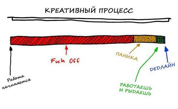
In order not to be like this ^, one must clearly and ironically (ironically) plan everything out.
- Preparation of TK (general concept, functions, elaboration of potential solutions, comparison with terms). There are a lot of jokes on the topic “what TK is such a solution”, but once again you shouldn’t ignore the reminder. The more detailed the TK, the fewer surprises will arise along the way. It is not necessary to understand electronics, but it is more than enough to describe what the device should do, what approximate dimensions, special components, budget, terms. If the engineers are a separate team, then you can draw up a commercial offer, where the engineers will describe your TK from the technical side (not for free, of course, because this is already serious work):
- method of implementation, for example, it can be a full-sized model with subsequent modifications to create a prototype or immediately a prototype (and this also happens, but I do not recommend it);
- output products (you can simply give away the working device, and you can also draw diagrams / drawings / assembly documentation);
- The task list usually describes the project life cycle;
- technical requirements for the device;
- pricing deadlines and payment.
Separate greetings to those who like not to properly explain the task, but asks to calculate the cost price. This is a stupid idea, since a preliminary assessment does not guarantee at all that it will fit into this amount; - Development of an approximate concept (pictures for bosses / sponsors). Most often, it is in haste selected element base and worn on the PCB to get a 3D model, to try it on the case and to please the boss. But this is only an approximate model, in 90% of cases something can go wrong (there is no necessary battery size, for example, or when tracing, it just doesn’t fit into these dimensions and you need to increase just a couple of mm or everything went too well and the board can be reduce);
- Development of Gantt charts / schedules / deadlines. One of the most important moments. The engineer needs to estimate the time and amount of tasks in the complex. There are intermediate stages of demonstration of the results, they also need to be announced, so that there are no surprises. Be sure to pledge risks. For example, one important element travels from abroad, paid for urgent delivery, but it was delayed somewhere. In addition, we all know that if there is no deadline, then all this is done without any enthusiasm, sluggish, long and tedious;
- Approval of the tasks with the team. Everything is painted, compiled, reviewing schedules and tasks again, discussing controversial points, signing / not signing papers and starting to work.
The life cycle of the development of PP
- Selection of the element base (which components will be laid). Analyzing prices, availability and delivery times. Selection is performed in dynamic mode with the creation of the scheme. The choice of the element base is carried out on the basis of a schematic electric circuit with regard to the conditions and requirements set forth in the TOR;
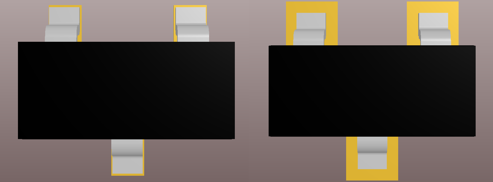
- Drawing components. The conditional graphic designation, footprint, 3D model, parameters are the components of any component. Different engineers conduct their libraries differently, some use ready-made ones. For me, the rule is meticulous drawing. The 3D model of the component allows you not only to roll out the 3D model of the board, but also to check the correctness of the seat. Under different technologies different seats. Different parameters (even if the denomination is simply different) are different components. This teases a lot of manual editing errors;
- Creating a schema. As there are rules for writing a readable code, so there are rules for creating a readable schema. The scheme can be divided into blocks, sign them, arrange the path of current flow. Specify pins that can be swapped. The more detailed the scheme, the fewer issues with the trace. If the device consists of several printed circuit boards, then it is much more convenient to maintain each circuit separately, but then you need to create an assembly circuit indicating how the boards are interconnected. However, all this is described in the standards;
- Approval of the scheme. Once again we check the element base, calculations, datasheets. It is better to spend 5-15 minutes once more than to cut the tracks and solder the sandwiches;
- Edit scheme as needed. Made changes, approved, and already at this stage you can roll out the BOM (list of elements) and order key chips, which probably will not change. Small things (resistors / capacitors / diodes etc) may vary;
- PCB tracing. If necessary, the circuit and the element base are adjusted. This is quite a creative process, you can trace, trace, and then score and start all over again. About autotras opinion is ambiguous, everything is done as they see fit. It is also important to take into account the production technology of the PCB when tracing, because if I know what I will do where quality does not shine, then I will not make ultra-thin tracks and small transitional ones;
- Approval of unstrived PP;
- Issuance of a 3D model of PP. Honestly, all customers love models, this is a win-win option if deadline is on the way. In addition, we give the model to our designers and they customize the body or grumble and ask you to change something;
- Preparation of gerber files for the manufacture of printed circuit boards. It is best to send a gerbera for production. Firstly, if you send just * .pcbdoc, then you can reverse engineer it. Secondly, in this case, the manufacturer is not responsible for how they prepare the gerbera, that is, if you gave * .pcbdoc and they accidentally deleted some polygon / component during the "conversion", then it was not their fault. Do not be lazy, prepare gerberas, check them in special programs. It is especially important to compare with the drill;
- Preparation of documentation. Standard documentation set: list of elements, specification, drawing, topology, installation documentation. It can be done according to GOST, according to foreign standards or on its own. If you are doing it your way, then it is better to adhere to unification, it will be easier to understand.
- The list of elements is needed both for the purchase and for the installer (basically, it’s enough to output the designator, component name, package, quantity, according to the presence / desire of value, marking). The markings do not indicate everything, but it simplifies the work of the installer, he does not have to think 30KOm is 303 or 304? The completeness of our documentation is all;
- Specification - all the components included in the product, the documentation included in this product is also noted here: assembly drawing of the printed circuit board, basic electric circuit, list of elements;
- Drawing - it can be a dimensional drawing or assembly. It can be useful for checking the PP after production or for finalizing the purchased case;
- Topology - needed to check the board. If the board is small or there are a lot of components on it, then it is best to check whether everything is correct, whether the manufacturer was wrong somewhere;
- Installation documentation - contour image of the product, as well as the data necessary for its installation (installation) at the place of use. The structure includes: the outline of the printed circuit board, topology, the image of the components (top view), marking, designation, sometimes a side or cross-section view, if the installation is complex. Do not forget about the keys on the components, it is also very important that then the installer did not arrange tantrums. My first motherboard somehow went away with my first documentation and here an aunt flies to the design office with a cry “Where is the plus and minutes for the diode?”. Or the customer himself soldered everything, complained that nothing worked, sent a photo, and the controller didn’t solder so much.
- The list of elements is needed both for the purchase and for the installer (basically, it’s enough to output the designator, component name, package, quantity, according to the presence / desire of value, marking). The markings do not indicate everything, but it simplifies the work of the installer, he does not have to think 30KOm is 303 or 304? The completeness of our documentation is all;
- Documentation approval
Writing a lower level program
The software life cycle depends on the specifics of the project, but basically everything follows the pattern:
- Requirements analysis;
- Algorithm development (creation of program operation logic);
- Writing source code;
- Compilation;
- Testing and debugging (a lot of debugging);
- Documentation.
It should be added that all the same, software development of the lower level and top-level software are different, since everything is very, very dependent on hardware. Nepapai, the quality of the board, components, the phase of the moon, anything can affect the correctness of the program, it is precisely because the software engineer is an engineer, he also has to tap the soldering iron on the keyboard, besides tapping on the keyboard.
Seriously, rinse your programmer as you like, but he must keep records. He was suddenly offered a better place or a cyclist moved - everything. Understanding another's code, no comments, no algorithm is unbearable pain, it's easier to write everything from scratch (and this is time and money).
A programmer, remember about karma, you hand over a project without commentaries, and once you get into the same one yourself!
Case drawing
We work together with the technical designer at the stage of tracing, because you need to approve that the board is satisfied and becomes a case before being sent to production. If the software allows, then it is most convenient to roll out the 3D model of the PCB. Designers have their own nuances, but you also need to take into account what material the body will be in, what method it will be produced (if already serial, you can make a mold or 3D printing for the layout) or it will be bought ready and just refined.
Why cycle?
I call all this a cycle, because this series of tasks (circuit, board, package, program) is an integral part of the product. Sometimes in order to reach the “product” finish point this task chain needs to be passed several times. Even inside the "series", too, everything is cyclical. When developing a scheme, you again and again return to the element base; from board to circuit; from the case to the board. And here and there. It probably looks like a web, a change in one node sometimes pulls changes in many others. Therefore, I use this term. If the labor engineers call it differently, write and I will correct it.
Production
Organization of production is also an important part, especially if you do not have your own shop. For everything about everything (the organization, not the production itself) it is better to allocate ~ a month, then we explain why.
When the approved scheme appeared, it’s time to take on the purchase of components, since not everything is available. As long as the board is not distributed, it is possible to make changes without any problems. Components are better to purchase from official suppliers and distributors. Of course, you can purchase in China, but if it is Chinese China, then half of the chips can be defective. The same applies to purchases on the sites of private ads.
There are many suppliers, if one LEDs are cheaper, it does not mean that everything is cheaper at it (yes, there are people who think that, and a remark for them). The most effective way to reduce prices and terms of different suppliers in the table. It is better to buy with a margin of 20-30% (there was a situation with transistors 0402, which were bought close to each other by quantity, and when soldering them with a hairdryer, it blows).
There are also nuances with supplies, for example, a module was needed, it is only in China, we need only a couple of dozen, but it is not profitable for suppliers to carry it (especially in such quantity), because they will spend too much money on receiving special documents. Because ordered by regular mail, there is a lot of time float. A recent rake taught one more thing: keep abreast of it, call your supplier every 3-5 days, because most often they themselves will not be notified that problems have occurred. This product travels from England, promised 5-9 business days. It took two weeks, okay, after a long embarrassment and attempts to justify, it turned out that at the time of ordering the goods in the warehouse was not (although they said that everything was in stock, everything was OK) and he just left and will be another week, and already need to run production. Circus Providers.
When the board is scattered, checked, we make out the gerber files and send it to production. But, there is also an underwater stone, there is usually a line in the production.
Manufacturers are different, there are those who make long and high quality, but there are those who are quick and not very high quality, but for a small batch of the layout. Everyone makes mistakes, ordered the boards at the best enterprise, all by Feng Shui, but here they come and in the place of the central pad of one of the mikruh (drumming) marking (silk-screen printing). There was one question: how? The deadlines allowed us to remake them, but the next time they even managed to remove one of the polygons. There are different situations, all the risks do not take into account, but you should be ready for them.
Installation. If the batches are large, it makes sense to order an automated installation or if these boards will be launched more than once into production. In any other case - manual installation. Enterprises take on small lots very reluctantly, because it is rather unprofitable.
If you are looking for installers yourself, it is better to ask in advance than solder about complex cases (for example, transistors in case 0402 or LGA-14), show the installer (make sure that the person will actually look at it, and then solder two vertically and closely resistors placed horizontally).
There is still need to mention that sometimes the question of the method of installation may arise at the stage of tracing. For example, there is a component in the SOT-23 package, but in the library for this building there are two seats - regular and from NXP; for microcircuits, landing can be with back and front mini.
Debugging
This is a very specific stage. Sometimes for debugging you need to assemble entire stands that are more expensive than the device. It may also be such that the concept of the board may depend on the debugging method, for example: the device consists of 3 boards and debugged each one separately before, and then everything was in a heap, but the administration offered to do all three boards in one piece and then break them. In this case, the device for debugging is one thing, but then you need to spend time on three boards and a new stand, it turned out not to be profitable (simply because then only one board was needed).
If errors were found during debugging, they are best documented so that you do not step on the same rake in the future.
Why is it all the better to start a project with a layout, rather than developing an experimental device / serial at once? Because in the case of the second, it is impossible to immediately say the matter as a board, element base or in soldering.
And do not forget about the use of power supplies.
Conclusion
The development of iron is long, expensive, difficult, but very, very interesting, you can write about it again and again. The main thing is not to forget the phrase " Do well, it will turn out badly itself ."
There are also plans to write articles about circuitry (from idea to scheme, where to start, how to do calculations, what you need to know and understand? That is, for beginners), tracing (drawing components, complex seating, life hacking, CAD tutorial ), soldering and rake with scaling production, if you are, of course, interested.

All with holidays and upcoming working days!
Source: https://habr.com/ru/post/319370/
All Articles