First steps with STM32 and mikroC compiler for ARM architecture - Part 2, continued
Having dealt with the timer, we will try to use it for something, except for the generation of time intervals. Most often with the help of a timer, a PWM signal is generated. What is it you can read in the vast web, for example, omniscient Wikipedia.
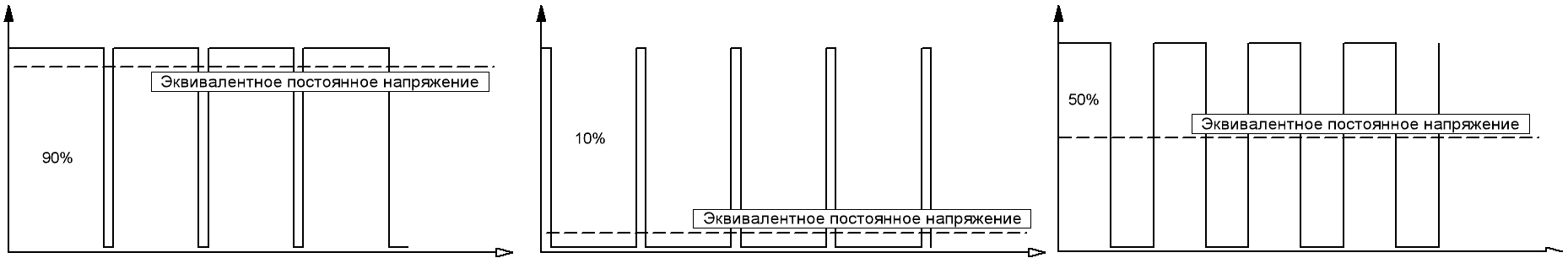
The main charm of PWM is that it allows you to change the effective value of the voltage applied to one or another load with the help of keys operating in a pulsed mode (most effective relative to energy loss). For a PWM signal, the main parameters are the total pulse duration and the duration of its active state (usually a high signal level).
The effective voltage value is dependent on the duration of the active state of the pulse. Our MK is able to generate PWM using the hardware functions of the timer, without taking the precious time of the processor core.
Using the MC as a PWM generator, you can control a powerful load (for example, a heater or an electric motor). To smooth the higher harmonics penetrating the load from the PWM modulator itself, you must use a LC or RC low pass filter.
One of the control circuits of the DC motor using the MK is shown below.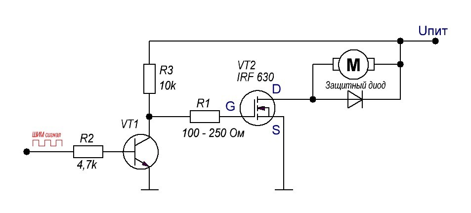
In this case, the motor itself having an inductive component of the load acts as a low-pass filter.
Each timer has 4 independently adjustable channels, each of which can be used to generate pulses ( compare mode ) or to capture them ( capature mode ). To begin, consider what configuration registers are needed in order to set our timer in the PWM signal generation mode:
TIMx_CR1 - Timer setting register.
In the last part, we already used the TIMx_CR1.CEN bit (enable / disable timer) of this register. Another important thing for us is the bit TIMx_CR1.DIR - the direction of the account. By default TIMx_CR1.CEN = 0 , the count is direct, the readings are incremented to the value 65535 or the value written to the register TIMx_ARR . When the TIMx_CR1.CEN = 1 bit is set , the counting is reversed; at each clock cycle of the incoming clock signal, the readings decrease from 65535 to 0 (or to the register value ( TIMx_ARR )).
TIMx_CCR1, TIMx_CCR2, TIMx_CCR3, TIMx_CCR4 - capture-compare registers.
Record values in them sets the duty cycle of PWM pulses. In the pulse capture mode, the value of the TIMx_CNT timer register is written to these cells when the pulse channel is fixed at the input of the corresponding channel.
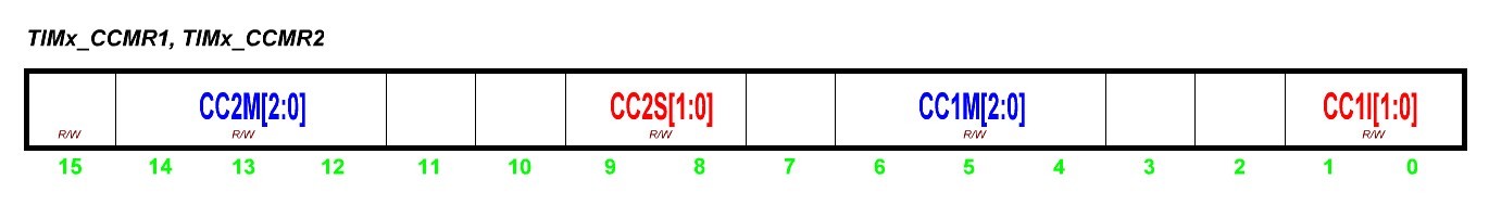
TIMx_CCMR1 , TIMx_CCMR2 - registers of the capture / generation channels.
Sets the timer operation mode as a source of pulses or a PWM signal, or as a pulse duration meter (capture mode). TIMx_CCMR1 refers to the 1st and 2nd channel of the timer, TIMx_CCMR2 - to 3 and 4. Next we will consider the register TIMx_CCMR1 , the settings for TIMx_CCMR2 are similar
TIMx_CCMR1.CC1S , used to enable the pulse generation mode or the pulse capture mode.
- TIMx_CCMR1.CC1S = 00 - the channel is operating in the pulse generation mode;
- TIMx_CCMR1.CC1S = 01 - the channel is in capture mode, the capture signal is TI1;
- TIMx_CCMR1.CC1S = 10 - the channel is in capture mode, the capture signal is TI2;
for TIMx_CCMR1.CC2S , similarly, except that
- TIMx_CCMR2.CC1S = 01 - the channel is in capture mode, the capture signal is TI2;
- TIMx_CCMR2.CC1S = 10 - the channel is in capture mode, the capture signal is TI1.
This setting is necessary to be able to connect to 2 signal channels from one input, which is used, for example, to capture the PWM signal.
The remaining bits of the TIMx_CCMR1 register depend on the generation mode or the capture mode. While our goal is to generate a PWM ( TIMx_CCMR1.CC1S = 00 ) signal, we will therefore describe the purpose of the main parameters for this mode of operation.
TIMx_CCMR1.CC1S , TIMx_CCMR1.CC2S - bits for setting the signal at the output of the corresponding timer channel.
- TIMx_CCMR1.CC1S = 000 - the match of the comparison register (CCR1) and the counting register (CNT) does not affect the state of the timer output;
- TIMx_CCMR1.CC1S = 001 - with CCR1 = CNT, the signal at the channel output = 1;
- TIMx_CCMR1.CC1S = 010 - with CCR1 = CNT, the signal at the channel output = 0;
- TIMx_CCMR1.CC1S = 010 - when CCR1 = CNT, the signal at the channel output is inverted;
- TIMx_CCMR1.CC1S = 100 - the output is always 0;
- TIMx_CCMR1.CC1S = 101 - the output is always 1;
- TIMx_CCMR1.CC1S = 110 - PWM mode number 1 (Direct PWM). If the counting register works on addition: when CNT <CCR1 the output signal = 1, otherwise 0. If the counting register works on subtraction: when CNT> CCR1 the output signal = 0, otherwise 1.
- TIMx_CCMR1.CC1S = 111 - PWM mode number 2 (Reverse PWM). If the counting register works on addition: for CNT <CCR1, the signal at the output = 0, otherwise 1. If the counting register works for subtraction: for CNT> CCR1, the output signal is 1, otherwise 0.
TIMx_CCER - A register that enables and disables the corresponding channel of signal generation / capture by a timer.
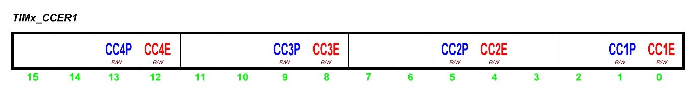
- TIMx_CCER1.CC1E, TIMx_CCER1.CC2E, TIMx_CCER1.CC3E, TIMx_CCER1.CC4E - enables and disables the corresponding generation / capture channel.
- TIMx_CCER1.CC1P, TIMx_CCER1.CC2P, TIMx_CCER1.CC3P, TIMx_CCER1.CC4P - inversion of the output signal polarity for the generation mode and selection of the leading or trailing edge of the pulse for the capture mode.
First you need to configure the microcontroller port to work with the timer output. This port mode is called: Alternate Function . To enable it in the microC there is a function:
GPIO_Alternate_Function_Enable(&module); where & module is a pointer to a module that implements an alternative I / O port function. For example, for channel 3 TIM3 is & _GPIO_MODULE_TIM3_CH3_PB0 , for channel 2 TIM2: & _GPIO_MODULE_TIM2_CH2_PA1 . In general, the pointer has the form & _GPIO_MODULE_TIMa_CHb_Pxy , where x is the port and y is the output to which the b-channel a-timer is connected according to the data for a specific microcontroller ( Code Assistsnt (ctrl-space) can help here) , enter _GPIO_ MODULE and select what we need from the drop-down list).
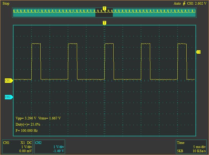
Let's try to generate a PWM signal with a 25% duty cycle at the PB0 pin of our microcontroller:
void main() { GPIO_Alternate_Function_Enable(&_GPIO_MODULE_TIM3_CH3_PB0); // 0 RCC_APB1ENRbits.TIM3EN=1; // TIM3 TIM3_PSC=7199; // 7200, 10 . TIM3_ARR=99; // 0 99, . 10000 / (99+1) = 100 . TIM3_CCR3=25; // 25 , 100 25 , 75 - . TIM3_CCERbits.CC3E=1; // 3 TIM3_CCMR2_Outputbits.OC3M=0b110; // - OC3M=110 - . TIM3_CR1bits.CEN=1; // while(1) { } } At the output of PB0, we get the following picture:
In microC, the PWM modulator can be configured using built-in functions. To do this, we first initialize the timer into the PWM modulator mode using the function
period = PWM_TIM_Init(freg); - freg is the frequency of operation of the PWM modulator in hertz;
- period - the function returns the period of our generator: the number of timer ticks for one period of the output signal, in fact the value of the TIM register register_ARR
After that, we establish the duty cycle of the generated pulses of the channel we need using the function:
PWM_TIM_Set_Duty(duty, _PWM_INVERTED /_PWM_NON_INVERTED, channel); - duty - the duty cycle of our PWM signal, in fact, the value of the register TIMx_CCRy , varies from 0 to the value of the period ;
- _PWM_INVERTED or _PWM_NON_INVERTED - direct or reverse shim;
- channel - channel PWM modulator, has the values:
- _PWM_CHANNEL1 - for 1 channel;
- _PWM_CHANNEL2 - for 2 channels;
- _PWM_CHANNEL3 - for 3 channels;
- _PWM_CHANNEL4 - for 4 channels;
Finally run our PWM generator function
PWM_TIM3_Start(channel, &module) - channel - PWM modulator channel;
- & module is a pointer to the module that outputs the PWM signal to the physical output of the microcontroller, the value is the same as we indicated when switching the port of the microcontroller using the GPIO_Alternate_Function_Enable (& module) command to Alternate Function mode for connecting the timer output to the MC output.
Let's write a simple program that increases the brightness of the LED built into our board when a button is pressed.
unsigned short state; // , 1 . unsigned int period; // unsigned short dutyled;// void main() { dutyled=10; // 10% GPIO_Alternate_Function_Enable(&_GPIO_MODULE_TIM3_CH4_PB1); // PB0 GPIO_Digital_Input(&GPIOb_BASE, _GPIO_PINMASK_8); period = PWM_TIM3_Init(5000); // 5000 PWM_TIM3_Set_Duty((period/100)*dutyled, _PWM_NON_INVERTED, _PWM_CHANNEL4); // 4 3 PWM_TIM3_Start(_PWM_CHANNEL4, &_GPIO_MODULE_TIM3_CH4_PB1); // 4 , PB1 while(1) { if (Button(&GPIOb_IDR, 8, 1, 1)) state.b1=1; if (state.b1 && Button(&GPIOb_IDR, 8, 1, 0)) { // state.b1= ~state.b1; dutyled = dutyled + 10; if (dutyled >= 100) // 100% 0 dutyled=10; PWM_TIM3_Set_Duty((period/100)*dutyled, _PWM_NON_INVERTED, _PWM_CHANNEL4); // } } } Now each time you press a button, our LED starts to glow brighter. The duty cycle of the PWM signal increases after each pressing by 10% - the LED brightness also increases.
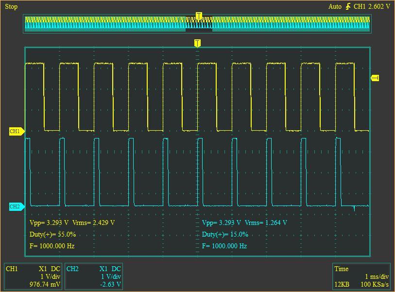
Using the built-in functions of microC, let's generate 2 PWM signals at the outputs of the CH2 (PA7) and CH3 (PB0) TIM3 channels with duty cycles of 15% and 55%, respectively.
unsigned int period, duty1, duty2; // void main() { duty1=55; // duty2=15; GPIO_Alternate_Function_Enable(&_GPIO_MODULE_TIM3_CH3_PB0); // PB0 GPIO_Alternate_Function_Enable(&_GPIO_MODULE_TIM3_CH2_PA7);// P7 period = PWM_TIM3_Init(1000); // 1000 PWM_TIM3_Set_Duty((period/100)*duty1, _PWM_NON_INVERTED, _PWM_CHANNEL3); // 3 3 PWM_TIM3_Set_Duty((period/100)*duty2, _PWM_NON_INVERTED, _PWM_CHANNEL2); // 2 3 PWM_TIM3_Start(_PWM_CHANNEL3, &_GPIO_MODULE_TIM3_CH3_PB0); // 3 , PB0 PWM_TIM3_Start(_PWM_CHANNEL2, &_GPIO_MODULE_TIM3_CH2_PA7); // 2 , PA7 while(1) { } By connecting the oscilloscope to the terminals PA7 and PB0, we can observe our signals:
The oscilloscope measures the effective values of RMS, and we can observe that they depend on the duty cycle of our pulses. This can be used to generate PWM arbitrary signals, such as sinusoids. Let's try to do it:
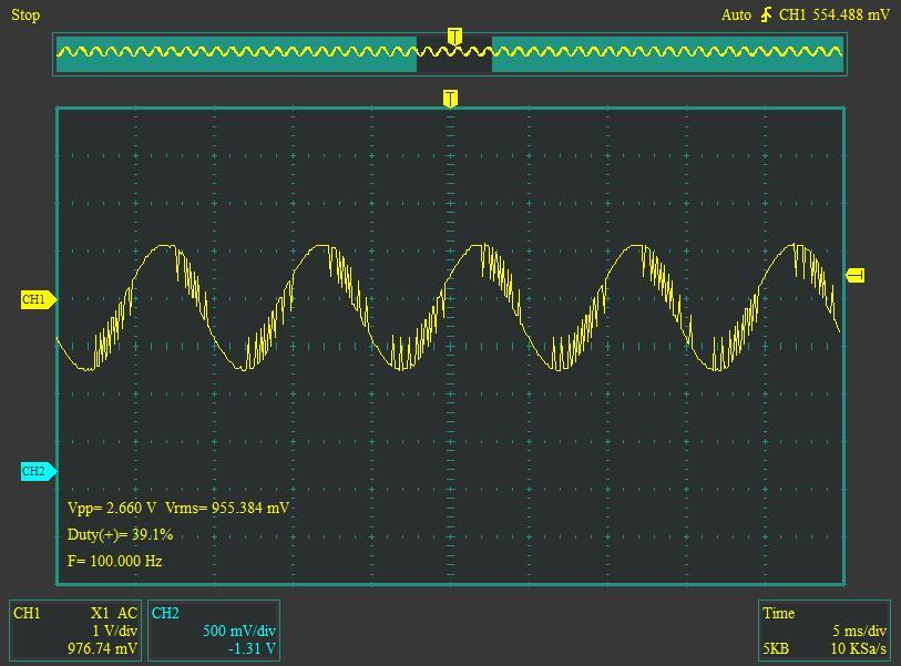
Timer 3 will generate a PWM signal, the duty cycle of which we will change according to the sinusoid law. For the experiment, we divide the period into 40 parts (in 9-degree increments) and calculate the sine values for them, and write the normalized PIMA period to the CCR register of the channel we need, thereby changing the pulse ratio and forming a sinusoid at the output of the pin of the MK timer. STM32 is sufficiently pre-production MK, so for low frequencies, of the order of 100 Hertz, you can use the SIN () Sishn function directly. Let's set up Timer 2 to call interrupts with a frequency of 4000 Hz. Considering that one period of a sinusoid takes 40 counts (360/9) in us, we should see a sinusoid with a frequency of 100 Hz on the oscilloscope screen.
unsigned int cpwm; // unsigned int ugol = 0; // const float PI=3.1416; // =3,1416 void main() { GPIO_Alternate_Function_Enable(&_GPIO_MODULE_TIM3_CH3_PB0); // 3 72 RCC_APB1ENRbits.TIM3EN=1; TIM3_CCERbits.CC3E=1; TIM3_CCMR2_Outputbits.OC3M=0b110; TIM3_CCR3 = 1000; TIM3_ARR = 1999; TIM3_PSC=0; TIM3_CR1bits.CEN=1; // 4 4000 RCC_APB1ENR.TIM4EN = 1; TIM4_CR1.CEN = 0; TIM4_PSC = 719; TIM4_ARR = 24; NVIC_IntEnable(IVT_INT_TIM4); // TIM4 TIM4_DIER.UIE = 1; // TIM4_CR1.CEN = 1; // 4 while(1) { } } void Timer2_interrupt() iv IVT_INT_TIM4 { TIM4_SR.UIF = 0;// cpwm= 1000 + (1000 * sin((PI*ugol)/180)); // TIM3_CCR3 = cpwm; // R ugol = ugol + 9; // 9 if (ugol > 359) ugol = 0; // sin } the signal from the output of our MK must be passed through a low-pass filter in order to cut off the frequency at which the PWM generator operates. Since the frequency of our sine wave is 100 Hz, the filter cut-off frequency is 300 Hz.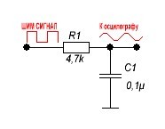
This is the signal that the oscillograph shows us:
This is the end of the second part of our series of articles. In the next part, I will try to talk about working with the serial interface UART, and try to use the capabilities of the MK to communicate with the GSM module.
')
Source: https://habr.com/ru/post/319256/
All Articles