Increase code performance: think first about data

Being engaged in graphics rendering programming, we live in a world in which low-level optimizations are required in order to achieve GPU frames with a length of 30 ms. To do this, we use various techniques and developed from scratch new rendering passes with enhanced performance (geometry attributes, texture cache, export, etc.), GPR compression, latency hiding, ROP ...
In the area of improving CPU performance, various tricks were used at one time, and it is noteworthy that today they are used for modern video cards to speed up ALU computations ( Low Level Optimization for AMD GCN , Fast Backward Square Root in Quake ).
')
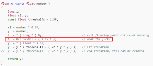
Quick square root in quake
But recently, especially in the light of the transition to 64 bits, I have noticed an increase in the number of non-optimized code, as if the industry is rapidly losing all the previously accumulated knowledge. Yes, old tricks like fast reverse square root on modern processors are counterproductive. But programmers should not forget about low-level optimizations and hope that the compilers will solve all their problems. They will not decide.
This article is not an exhaustive hardcore iron guide. This is just an introduction, a reminder, a set of basic principles for writing effective code for the CPU. I want to “ show that low-level thinking is still useful today, ” even if it’s about processors that I could add.
In this article, we will look at caching, vector programming, reading and understanding assembly code, and writing code that is convenient for the compiler.
Why bother?
Do not forget about breaking
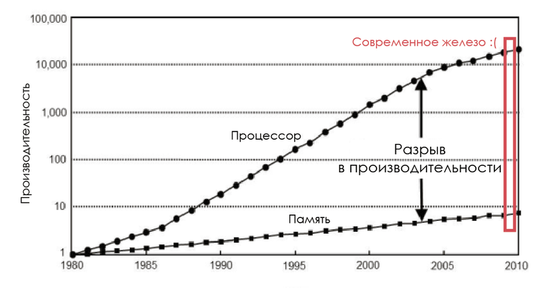
In the 1980s, the memory bus frequency was equal to the CPU frequency, and the delay was almost zero. But processor performance grew logarithmically in accordance with Moore's law, and the performance of RAM chips increased disproportionately, so that memory soon became a bottleneck. And the point is not that it is impossible to create a faster memory: it is possible, but economically unprofitable.
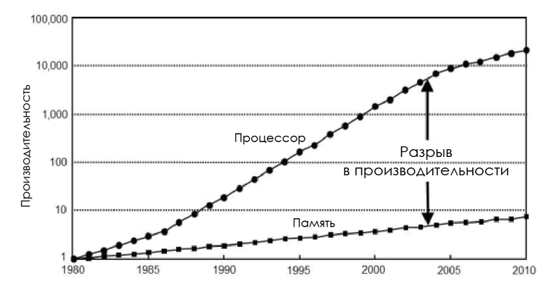
Change processor speed and memory
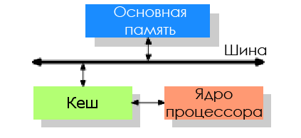
To reduce the impact of memory performance, CPU developers have added a tiny amount of this very expensive memory between the processor and the main memory - this is how the processor cache appeared.
The idea is this: there is a good chance that the same code or data may again be required in a short period of time.
- Spatial locality: loops in code, so that the same code is executed time after time.
- Temporal locality: even if the memory areas used for short periods of time are not adjacent to each other, there is still a high probability that the same data will soon be used again.
CPU cache is a complex method of increasing productivity, but without the help of a programmer, it will not work correctly. Unfortunately, many developers do not realize the cost of using memory and CPU cache structure.
Data-oriented architecture
We are interested in game engines. They process increasing amounts of data, transform them and display them in real time. Considering this, as well as the need to solve problems with efficiency, the programmer must understand what data he processes and know the equipment with which his code will work. Therefore, he must be aware of the need to implement a data-oriented architecture (DoD).
Or maybe the compiler will do it for me?
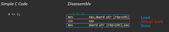
Simple addition. On the left - C ++, on the right - the resulting code in assembler
Let's look at the above example for an AMD Jaguar processor (similar to those used in game consoles) (useful links: AMD's Jaguar Microarchitecture: Memory Hierarchy , AMD Athlon 5350 APU and AM1 Platform Review - Performance - System Memory ):
- Load operation (about 200 cycles without caching )
- Actual work: inc eax (1 cycle)
- Storage operation (~ 3 cycles, same cache line)
Even in such a simple example, most of the processor time is spent waiting for data, and in more complex programs, the situation does not get better until the programmer pays attention to the basic architecture.
In short, compilers:
- They do not see the whole picture; it is very difficult for them to predict how the data will be organized and how they will be accessed.
- Arithmetic operations can be well optimized, but sometimes these operations are just the tip of the iceberg.
The compiler has quite a bit of room for maneuver when it comes to optimizing memory access. The context is known only to the programmer, and only he knows what code he wants to write. Therefore, you need to understand the flow of information flows and first of all proceed from data processing in order to squeeze everything possible from modern CPUs.
Brutal Truth: OOP vs. DoD

Impact of memory access on performance (Mike Acton GDC15)
Object-oriented programming (OOP) today is the dominant paradigm, it is her who is first of all studied by future programmers. It makes you think in terms of real-world objects and their relationships.
In a class, code and data are usually encapsulated, therefore an object contains all its information. Forcing to use arrays of structures (array of structures) and arrays * of pointers to * structures / objects, OOP violates the principle of spatial locality , on which cache memory acceleration is based. Remember the gap between processor and memory performance?
Excessive encapsulation is detrimental when working on modern hardware.
I want to tell you that when developing software, you need to shift the focus from the code itself to understanding data transformations, as well as respond to the current programming culture and state of affairs imposed by OO supporters.
In conclusion, I want to quote three big lies told by Mike Acton (Mike Acton) ( CppCon 2014: Mike Acton, "Data-Oriented Design and C ++" )
Software is a platform- You need to understand the hardware you are working with.
The code architecture is formed according to the model of the world.- The code architecture must conform to the data model.
Code is more important than data- Memory is a bottleneck, data is by far the most important thing.
Study iron
Microprocessor cache
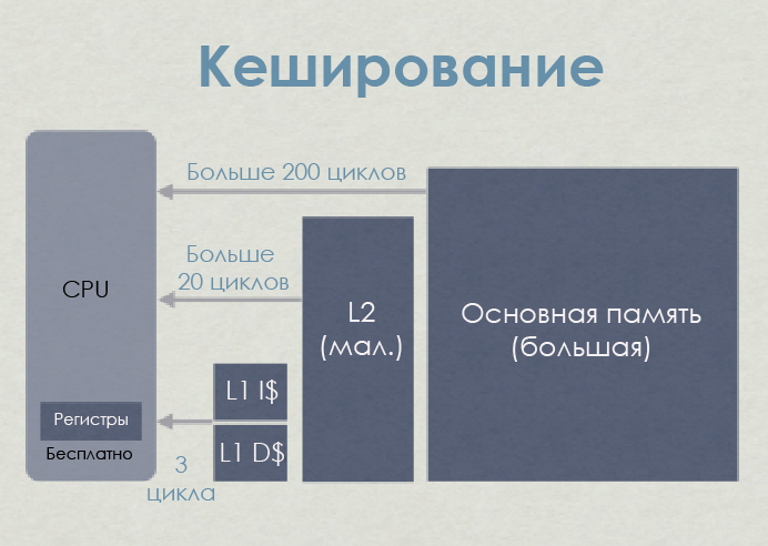
The processor is not physically connected directly to the main memory. All operations with RAM (loading and storage) on modern processors are performed through the cache.
When the processor is busy with a call (load) command, the memory controller first searches the cache for an entry with a tag corresponding to the memory address at which it needs to read. If such a record is found — that is, a cache hit occurs — then the data can be loaded directly from the cache. If not - cache miss , - the controller will try to extract data from lower cache levels (for example, first L1D, then L2, then L3) and, finally, from RAM. Then the data will be stored in L1, L2 and L3 ( inclusive cache ).
Memory Console Delay - Jason Gregory
In this simplified illustration, the processor (AMD Jaguar, used in PS4 and XB1) has two cache levels - L1 and L2. As you can see, not just data is cached, L1 is divided into code instruction cache (code instruction) (L1I) and data cache (L1D). The memory areas needed for code and data are independent of each other. In general, L1I creates far fewer problems than L1D.
In terms of latency, L1 is orders of magnitude faster than L2, which is 10 times faster than main memory. It looks sad in numbers, but not for every slip of the cache you have to pay the full price. You can reduce costs by hiding latency, dispatching, and so on, but this is beyond the scope of the post.
Memory Delay - Andreas Fredriksson
Each entry in the cache - the cache line - contains several adjacent words (64 bytes for AMD Jaguar or Core i7). When the CPU executes the instruction that retrieves or saves the value, the entire cache line is transferred to L1D. In the case of saving, the cache line to which an entry is made is marked as dirty until it is written back to RAM.
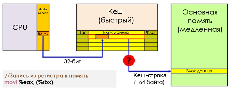
Write from register to memory
To be able to load new data into the cache, it is almost always necessary to first free up space by evicting the (evict) cache line .
- Exclusive cache: when retrieving, the cache line is moved from L1D to L2. This means that space must be allocated in L2, which may lead to the transfer of data back to main memory. Moving a retrieved string from L1D to L2 affects the latency of a cache miss.
- Inclusive cache: each cache line in L1D is also represented in L2. Extraction from L1D is much faster and requires no further action.
Fresh processors from Intel and AMD use inclusive cache . At first, this may seem like a wrong decision, but it has two advantages:
- It reduces latency when a cache misses, since there is no need to move the cache line to another level when retrieving.
- If one kernel needs data with which another kernel works, then it can extract the latest version from the upper levels of the cache without interrupting the work of another kernel. Therefore, inclusive cache has become very popular with the development of multicore architectures.
Cash line collisions: although several cores can efficiently read cache lines, write operations can lead to poor performance. False sharing means that different cores can change independent data in the same cache line. According to cache coherence protocols, if the kernel writes to the cache line, then a line in another kernel referring to the same memory is considered invalid ( cache slip , cache trashing). As a result, at each write operation memory locks occur. False separation can be avoided by making different kernels work with different strings (using extra space - extra padding, aligning the structures with 64 bytes, and so on).
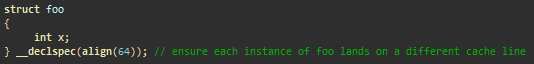
We avoid false division by writing data to different cache lines in each thread.
As you can see, understanding the hardware architecture is the key to finding and fixing problems that might otherwise go unnoticed.
Coreinfo is a command-line utility. It provides detailed information about all instruction sets stored in the processor, as well as reports which caches are assigned to each logical processor. Here is an example for a Core i5-3570K:
*--- Data Cache 0, Level 1, 32 KB, Assoc 8, LineSize 64 *--- Instruction Cache 0, Level 1, 32 KB, Assoc 8, LineSize 64 *--- Unified Cache 0, Level 2, 256 KB, Assoc 8, LineSize 64 **** Unified Cache 1, Level 3, 6 MB, Assoc 12, LineSize 64 -*-- Data Cache 1, Level 1, 32 KB, Assoc 8, LineSize 64 -*-- Instruction Cache 1, Level 1, 32 KB, Assoc 8, LineSize 64 -*-- Unified Cache 2, Level 2, 256 KB, Assoc 8, LineSize 64 --*- Data Cache 2, Level 1, 32 KB, Assoc 8, LineSize 64 --*- Instruction Cache 2, Level 1, 32 KB, Assoc 8, LineSize 64 --*- Unified Cache 3, Level 2, 256 KB, Assoc 8, LineSize 64 ---* Data Cache 3, Level 1, 32 KB, Assoc 8, LineSize 64 ---* Instruction Cache 3, Level 1, 32 KB, Assoc 8, LineSize 64 ---* Unified Cache 4, Level 2, 256 KB, Assoc 8, LineSize 64 Here the 32 KB L1 cache, 32 KB L1 cache, 256 KB L2 cache, and 6 MB L3 cache. In this architecture, L1 and L2 are assigned to each core, and L3 is shared by all cores.
In the case of AMD Jaguar CPU, each core has a dedicated L1 cache, and L2 is shared by groups of 4 cores in clusters (there is no L3 in the Jaguar).
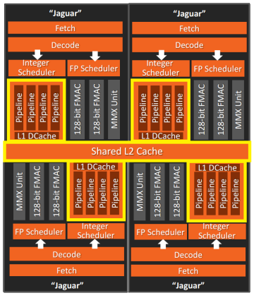
4-core cluster (AMD Jaguar)
When working with such clusters, special care should be taken. When a kernel writes to a cache line, it may become invalid in other kernels, which reduces performance. Moreover, with such an architecture, everything can become even worse: the kernel extracting data from the nearest L2 located in the same cluster takes about 26 cycles , and retrieving another cluster from L2 can take up to 190 cycles . Comparable to the extraction of data from RAM!
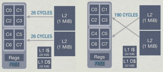
L2 latency in clusters in AMD Jaguar - Jason Gregory
For more information on cache consistency, see the Cache Coherency Primer article.
Assembly Basics
x86-64 bits, x64, IA-64, AMD64 ... or the birth of the x64 architecture
Intel and AMD have developed their own 64-bit architectures: AMD64 and IA-64. IA-64 is very different from x86-32 processors in the sense that it does not inherit anything from the x86 architecture. Applications for x86 should work on IA-64 through the emulation layer, therefore, they have poor performance on this architecture. Due to lack of compatibility with x86, IA-64 never took off, except for the commercial sphere. On the other hand, AMD has created a more conservative architecture, expanding its existing x86 with a new set of 64-bit instructions. Intel, who lost the 64-bit war , was forced to introduce the same extensions into its x86 processors . In this section, we look at x86-64 bits, also known as x64 architecture, or AMD64.
For many years, PC programmers have used x86 assembler to write high-performance code: mode'X ' , CPU-Skinning, collisions, software rasterizers (software rasterizers) ... But 32-bit computers were slowly replaced by 64-bit ones, and the assembler code also changed .
Know the assembler is necessary if you want to understand why some things work slowly and others quickly. It will also help you understand how to use intrinsic- functions to optimize critical parts of the code, and how to debug optimized (for example, -O3) code when debugging at the source code level no longer makes sense.
Registers
Registers are small fragments of very fast memory with an almost zero delay (usually one processor cycle). They are used as internal processor memory. They store data directly processed by processor instructions.
The x64 processor has 16 general-purpose registers (GPR). They are not used to store specific data types, and at the time of execution they contain operands and addresses.
In x64, eight x86 registers are expanded to 64 bits, and 8 new 64-bit registers are added. The names of 64-bit registers begin with r. For example, the 64-bit extension eax (32-bit) is called rax . New registers are named from r8 to r15 .

General architecture (software.intel.com)
The x64 registers include:
- 16 64-bit general purpose registers (GPR), of which the first eight are called rax, rbx, rcx, rdx, rbp, rsi, rdi and rsp. The second eight: r8 — r15.
- 8 64-bit MMX registers (a set of MMX instructions) covering the floating-point registers fpr (x87 FPU).
- 16 128-bit vector XMM-registers (set of SSE instructions).
In newer processors:
- 256-bit YMM registers (set of AVX instructions) that extend XMM registers.
- 512-bit ZMM-registers (set of AVX-512 instructions), extending XMM-registers and increasing their number to 32.
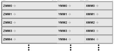
Relationships between ZMM, YMM, and XMM Registers
For historical reasons, several GPRs are called differently. For example, ax was an Accumulator register, cx - Counter, dx - Data. Today, most of them have lost their specific purpose, with the exception of rsp (Stack Pointer) and rbp (Base Pointer), which are reserved for managing the hardware stack (hardware stack) (although rbp can often be “optimized” and used as a GRP - omit frame pointer in Clang).
The low bits of the x86 registers can be accessed using subregisters . In the case of the first eight x86 registers, legacy names are used. Newer registers (r8 — r15) use the same, only simplified approach:
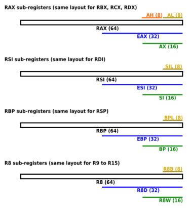
Named scalar registers
Addressing
When assembler instructions require two operands, usually the first is the destination, and the second is the source. Each of them contains the data to be processed, or the address of the data. There are three main addressing modes:
- Immediate
- mov eax, 4 ; moves 4 to eax
- From register to register
- mov eax, ecx ; moves the contents of ecx to eax
- Indirect:
- mov eax, [ebx] ; moves 4 bytes (eax size) to ebx address in eax
- mov byte ptr [rcx], 5 ; moves 5 to byte at rcx
- mov rdx, dword ptr [rcx + 4 * rax] ; moves dword to rcx + 4 * rax to rdx
dword ptr is called a size directive. It tells the assembler what size to take if there is an uncertainty in the size of the memory area to which it is referenced (for example: mov [rcx] , 5: should write byte? Dword?).
This can mean: byte (8-bit), word (16-bit), dword (32-bit), qword (64-bit), xmmword (128-bit), ymmword (256-bit), zmmword (512- bit).
SIMD instruction sets
Scalar implementation refers to operations with one pair of operands at a time. Vectorization is the process of transforming an algorithm, when instead of working with single pieces of data at a time, it begins to process several portions at a time (below we will see how it does it).
Modern processors can take advantage of a set of SIMD instructions (vector instructions) for parallel data processing.
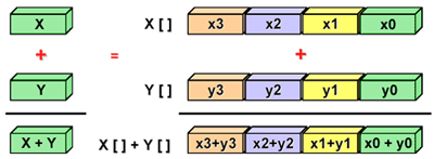
SIMD processing
SIMD instruction sets, which are available in x86 processors:
- Multimedia eXtension (MMX)
- Legacy It supports arithmetic operations on integer values packed in 64-bit vector registers.
- Streaming SIMD Extensions (SSE)
- Arithmetic operations on floating-point numbers packed in 128-bit vector registers. Integer and double precision support has been added to SSE2.
- Advanced Vector Extensions (AVX) - x64 only
- Added support for 256-bit vector registers.
- AVX-512 - x64 only
- Added support for 512-bit vector registers.
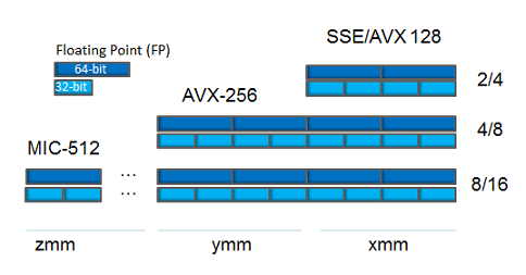
Vector registers in x64 processors
Game engines typically spend 90% of their execution time on running small portions of the codebase, mainly iterating and processing data. In such scenarios, SIMD can make a big difference. SSE instructions are usually used for parallel processing of sets of four floating point values packed into 128-bit vector registers.
SSE is mainly focused on the vertical representation (structure of arrays - Structure of Arrays, SoA) of data and their processing. But in general, the performance of SoA compared to Array of Structures (AoS) depends on the memory access patterns.
- AoS is probably the most natural option, easy to write. Satisfies the OOP paradigm.
- AoS has better data locality if all members are accessed together.
- SoA offers more possibilities for vectorization (vertical processing).
- SoA often uses less memory due to padding only between arrays.
// Array Of Structures struct Sphere { float x; float y; float z; double r; }; Sphere* AoS; ( 8 ): ------------------------------------------------------------------ | x | y | z | r | pad | x | y | z | r | pad | x | y | z | r | pad ------------------------------------------------------------------ // Structure Of Arrays struct SoA { float* x; float* y; float* z; double* r; size_t size; }; : ------------------------------------------------------------------ | x | x | x ..| pad | y | y | y ..| pad | z | z | z ..| pad | r.. ------------------------------------------------------------------ AVX is a natural extension of SSE. The size of vector registers is increased to 256 bits, which means that up to 8 floating point numbers can be packed and processed in parallel. Intel processors initially support 256-bit registers, and there may be problems with AMD. AMD's early AVX processors, such as Bulldozer and Jaguar, decompose 256-bit operations on 128-bit pairs, which increases latency compared to SSE.
In conclusion, I’ll say that it’s not so easy to rely solely on AVX (maybe for internal tools, if your computers run on Intel), and AMD processors for the most part do not support them natively. On the other hand, on any x64 processors, you can a priori rely on SSE2 (this is part of the specification).
Extraordinary performance
If the pipeline (pipeline) of the processor is operating in an extraordinary execution mode (Out-of-Order, OoO) and the execution of instructions is delayed due to the unavailability of the necessary input data, then the processor tries to find later instructions whose input data are ready to perform first out of turn.
The instruction cycle (or the cycle “receiving - decoding - execution”) is the process during which the processor receives instructions from the memory, determines what needs to be done with it, and executes it. The execution cycle of the command in the extraordinary execution mode looks like this:
- Receive / Decode : The instruction is retrieved from L1I (instruction cache). It is then transformed into smaller operations called microoperations , or µops.
- Renaming: due to existing dependencies between the register and the data, execution lock may occur. To solve this problem and eliminate false dependencies, the processor provides a set of unnamed internal registers used for current calculations. Register renaming is the process of converting references to architectural registers (logical) into references to unnamed registers (physical).
- Reorder Buffer: it contains pending micro-operations, stored in the order of receipt, as well as already completed, but not yet retired .
- Dispatching: micro-operations stored in the reordering buffer can be transferred in any order to parallel execution modules , taking into account dependencies and data availability. The result of the micro-operation is written back to the reordering buffer along with the micro-operation itself.
- Firing: a retirement unit constantly checks the status of micro-operations in the buffer, writes the results of the executed micro-operations back to the architectural registers (accessible to the user), and then removes the micro-operations from the buffer.
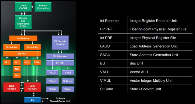
AMD Jaguar processor architecture
In the AMD Jaguar processor architecture, we can detect all the above blocks. For integer conveyor:
- "Decode and Microcode ROMs"
- = receive / decode module
- "Int Rename" and "Int PRF" (physical register file)
- = rename module
- The Retirement Control Unit (RCU), not shown here, controls the renaming of registers and the retirement of micro-operations.
- Dispatchers
- Internal dispatcher (Int Scheduler, ALU)
- It can transfer one micro-operation to the conveyor (two ALU-modules of execution I0 and I1) in an extraordinary order.
- AGU dispatcher (loading / storage)
- It can transfer one micro-operation to the conveyor (two AGU-modules of the LAGU b SAGU version) in an extraordinary order.
- Internal dispatcher (Int Scheduler, ALU)
Examples of micro-operations:
µops add reg, reg 1: add add reg, [mem] 2: load, add addpd xmm, xmm 1: addpd addpd xmm, [mem] 2: load, addpd Looking at the AMD Jaguar section in the wonderful instruction table on the Agner website , we can understand what the execution pipeline for this code looks like:
mov eax, [mem1] ; 1 - load imul eax, 5 ; 2 - mul add eax, [mem2] ; 3 - load, add mov [mem3], eax ; 4 - store (Jaguar) I0 | I1 | LAGU | SAGU | FP0 | FP1 | | 1-load | | | 2-mul | | 3-load | | | | 3-add | | | | | | | 4-store | | Here, breaking instructions in micro-operations allow the processor to take advantage of parallel execution modules, partially or completely “hiding” the delay in executing the instruction (
3-load and 2-mul are executed in parallel, in two different modules).But this is not always possible. The chain of dependencies between
2-mul , 3-add and 4-store does not allow the processor to reorganize these micro-operations ( 4-store needs the result 3-add , and 3-add needs the result 2-mul ). So for efficient use of parallel execution modules, avoid long chains of dependencies.Visual Studio Options
To illustrate the compiler-generated assembler, I will use msvc ++ 14.0 (VS2015) and Clang. I strongly recommend that you do the same and get used to comparing different compilers. This will help to better understand how all the components of the system interact with each other, and form their own opinion about the quality of the generated code.
A few goodies:
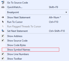
- The Show Symbol Names option can show the names of local variables and functions in disassembled form, instead of instructions or stack addresses.
- Make the assembler more readable:
- Project settings> C / C ++> Code Generation> Basic Runtime Checks , change the value to Default .
- Write the result to the .asm file:
- Project settings> C / C ++> Output Files> Assembler Output , make the value Assembly With Source Code .
- Lowering the frame pointer (Frame-Pointer omission) tells the compiler that ebp should not be used to control the stack:
- / Oy (x86 only, in Clang: -fomit-frame-pointer, works in x64)
Basic examples of disassembling
Here we look at very simple C ++ code samples and their disassembly. All assembler code is reorganized and fully documented to make it easier for beginners, but I recommend checking if you have any doubts about what the instructions are doing.
For ease of perception, prologues and epilogues of functions have been removed; we will not discuss them here.
Note: local variables are declared on the stack. For example, mov dword ptr [rbp + 4], 0Ah; int b = 10 means that the local variable 'b' is pushed onto the stack (referenced by rbp) at a relative address (offset) 4 and initialized as 0Ah, or 10 in decimal expression.
Floating point arithmetic with simple precision
Floating-point arithmetic can be performed using x87 FPU (80-bit precision, scalar) or SSE (32-bit or 64-bit precision, vectorized). In x64, the SSE2 instruction set is always supported, and by default it is used for floating-point arithmetic.
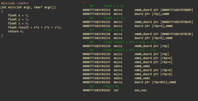
Simple floating point arithmetic using SSE. msvc ++
Initialization
- movss xmm0 , dword ptr [adr]; loads floating point value located at adr address in xmm0
- movss dword ptr [rbp], xmm0 ; saves it to the stack (float x)
- ...; same with y and z
Calculates x * x
- movss xmm0 , dword ptr [rbp] ; loads scalar x to xmm0
- mulss xmm0 , dword ptr [rbp] ; multiplies xmm0 (= x) by x
Calculates y * y and adds to x * x
- movss xmm1 , dword ptr [rbp + 4] ; loads scalar y to xmm1
- mulss xmm1 , dword ptr [rbp + 4] ; multiplies xmm1 (= y) by y
- addss xmm0, xmm1 ; adds xmm1 (y * y) to xmm0 (x * x)
Calculates z * z and adds to x * x + y * y
- movss xmm1 , dword ptr [rbp + 8]; loads scalar z into xmm1
- mulss xmm1 , dword ptr [rbp + 8]; multiplies xmm1 (= z) by z
- addss xmm0, xmm1 ; adds xmm1 (z * z) to xmm0 (x * x + y * y)
Saves the final result
- movss dword ptr [ rbp + 0Ch], xmm0 ; saves xmm0 to the result
- xor eax, eax ; eax = 0. eax contains the return value of main ()
In this example, XMM registers are used to store a single floating point value. SSE allows you to work with both single and multiple values, with different data types. Look at the SSE addition instruction:
- addss xmm0, xmm1 ; each register as 1 scalar floating point value with single precision ( s calar ingle precision floating-point value)
- addps xmm0, xmm1 ; each register as 4 packed floating point values with single precision ( p acked s ingle precision floating-point values)
- addsd xmm0, xmm1 ; each register as a double-precision scalar value with double precision ( s calar d ouble precision floating-point value)
- addpd xmm0, xmm1 ; each register as 2 packed double-precision floating-point values ( p acked d double precision floating-point values)
- paddd xmm0, xmm1 ; each register as 4 packed dword-values ( p acked d ouble word (32-bit integer) values)
Branching
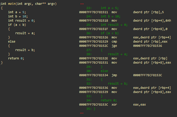
An example of branching. msvc ++
Initialization
- mov dword ptr [ rbp ], 5; saves 5 to the stack (integer a)
- mov dword ptr [ rbp +4], 0Ah; saves 10 to the stack (integer b)
- mov dword ptr [ rbp +8], 0; saves 0 to the stack (integer result)
Condition
- mov eax , dword ptr [ rbp +4]; loads b into eax
- cmp dword ptr [ rbp ], eax ; compares a with eax (b)
- jge @ ECF81536; makes the transition if a is greater than or equal to b
'then' result = a
- mov eax , dword ptr [ rbp ]; loads a into eax
- mov dword ptr [ rbp +8], eax ; saves eax to stack (result)
- jmp @ ECF8153C; moves to ECF8153C
'else' result = b
- (ECF81536) mov eax , dword ptr [ rbp +4]; loads b into eax
- mov dword ptr [rbp + 8], eax; saves eax to stack (result)
- (ECF8153C) xor eax, eax; eax = 0. eax contains the return value of main ()
The cmp instruction compares the operand of the first source with the second, sets the status flags in the RFLAGS register according to the result. Register ®FLAGS is a register of the status of x86-processors, containing the current state of the processor. The cmp instruction is usually used in conjunction with a conditional branch (for example, jge ). The condition codes used by the transitions depend on the result of the cmp instruction ( RFLAGS condition codes).
Arithmetic operations with integer and 'for' loop
In assembly language, cycles are represented mainly as a series of conditional jumps (= if ... goto).
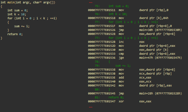
Arithmetic operations with integer and 'for' loop. msvc ++
Initialization
- mov dword ptr [ rbp ], 0; saves 0 to the stack (integer sum)
- mov dword ptr [k], 0Ah; saves 10 to the stack (integer k)
- mov dword ptr [ rbp +8], 0; saves 0 to the stack (integer i) for iteration in a loop
- jmp main + 30h; moves to main + 30h
The part of the code responsible for incrementing i
- (main + 28h) mov eax , dword ptr [ rbp +8]; loads i into eax
- inc eax ; increment
- mov dword ptr [ rbp +8], eax ; saves back to the stack
The part of the code responsible for testing the exit condition (i> = k)
- (main + 30h) mov eax , dword ptr [k]; loads k from the stack to eax
- cmp dword ptr [ rbp +8], eax ; compare i with eax (= k)
- jge main + 47h; makes the transition (ends the cycle) if i is greater than or equal to k
“Real Work”: sum + = i
- mov eax , dword ptr [ rbp +8]; loads i into eax
- mov ecx , dword ptr [ rbp ]; loads the amount into ecx
- add ecx, eax ; add eax with ecx (ecx = sum + i)
- mov eax, ecx ; transfers ecx to eax
- mov dword ptr [rbp], eax ; saves eax (amount) back to stack
- jmp main + 28h; makes the transition and processes the next iteration of the loop
- (main + 47h) xor eax, eax ; eax = 0. eax contains the return value of main ()
Built-in functions (intrinsics) SSE
, SSE ( — ). , :
- _mm_mul_ps mulps
- _mm_load_ps movaps
- _mm_add_ps addps
- _mm_store_ps movaps
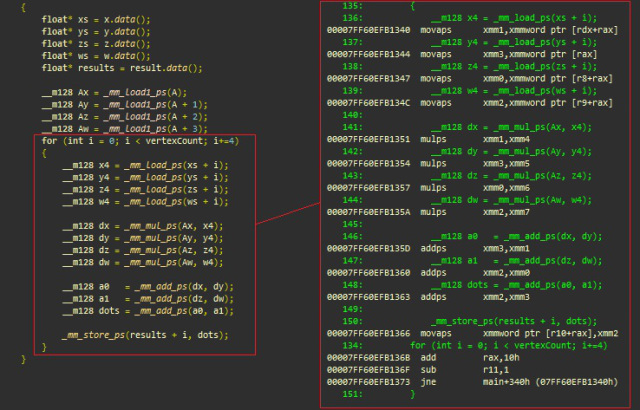
SSE, msvc++
(xmmword 128 dword)
- (main+340h) movaps xmm1 , xmmword ptr [rdx+rax] ; 128- xmmword ( ) xs+i xmm1
- movaps xmm3 , xmmword ptr [rax] ; 4 ys+i xmm3
- movaps xmm0 , xmmword ptr [r8+rax] ; 4 zs+i xmm0
- movaps xmm2 , xmmword ptr [r9+rax] ; 4 ws+i xmm2
dot(v[i], A) = xi * Ax + yi * Ay + zi * Az + wi * Aw , (vertices) :
- mulps xmm1, xmm4 ; xmm1 *= xmm4 xn.Ax, n [0..3]
- mulps xmm3, xmm5 ; xmm3 *= xmm5 yn.Ay, n [0..3]
- mulps xmm0, xmm6 ; xmm0 *= xmm6 zn.Az, n [0..3]
- mulps xmm2, xmm7 ; xmm2 *= xmm7 wn.Aw, n [0..3]
- addps xmm3, xmm1 ; xmm3 += xmm1 xn.Ax + yn.Ay
- addps xmm2, xmm0 ; xmm2 += xmm0 zn.Az + wn.Aw
- addps xmm2, xmm3 ; xmm2 += xmm3 xn.Ax + yn.Ay + zn.Az + wn.Aw
( + )
- movaps xmmword ptr [r10 + rax], xmm2 ; 128- xmmword (4 ) , r10+rax
- add rax , 10h; 16 rax ( = 4 )
- sub r11,1 ; r11–,
- jne main+34h;
AVX (256-, 8 ):
_m256 Ax = _mm256_broadcast_ss(A); ... for (int i = 0; i < vertexCount; i+=8) // 8 (256-) { __m256 x4 = _mm256_load_ps(xs + i); .. __m256 dx = _mm256_mul_ps(Ax, x4); .. __m256 a0 = _mm256_add_ps(dx, dy); .. _mm256_store_ps(results + i, dots); } (switch)
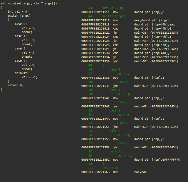
. msvc++
- mov dword ptr [ rbp ], 0; 0 ( )
- mov eax , dword ptr [argc]; argc eax
- mov dword ptr [ rbp +44h], eax ;
Conditions
- cmp dword ptr [ rbp +44h], 0; argc to 0
- je main+38h; if argc == 0, main+38h (case 0)
- cmp dword ptr [ rbp +44h], 1; argc 1
- je main+41h; if argc == 1, main+41h (case 1)
- cmp dword ptr [ rbp +44h], 2; argc 0
- je main+4Ah; if argc == 2, main+4Ah (case 2)
- cmp dword ptr [ rbp +44h], 3; argc 3
- je main+53h; if argc == 3, main+53h (case 3)
- jmp main+5Ch; main+5Ch ( )
Case 0
- (main+38h) mov dword ptr [ rbp ], 1; 1 (val)
- jmp main+63h; main+63h,
Case 1
- (main+41h) mov dword ptr [ rbp ], 3; 3 (val)
- jmp main+63h; main+63h,
...
- (main+63h) xor eax, eax ; eax = 0. eax main()
. ++- if-else, . .
useful links
- What Every Programmer Should Know About Memory
- Intel Instrinsics Guide
- Jaguar Out-of-Order Scheduling
- The Intel Architecture Processors Pipeline
- x86-64bit Opcode and Instruction Reference
- Why do CPUs have multiple cache levels?

Source: https://habr.com/ru/post/319194/
All Articles