A new type of hackathon has been tried in Kiev, it is planned to repeat this experience in Russia
At the Kiev Polytechnic Institute, a new type of hackathon was passed, with simultaneous development of both software (C, assembler) and circuitry (Verilog) parts of the system, synthesized for implementation in reconfigurable logic chips (FPGA / FPGA). Hackathon was also supported by one of the departments of the Kiev National University and Imagination Technologies, the developer of the PowerVR graphics processor inside the Apple iPhone. The result of the hackathon exceeded expectations (more on this below), and now plans are being developed to repeat it in other places, in particular in Tomsk or Novosibirsk.

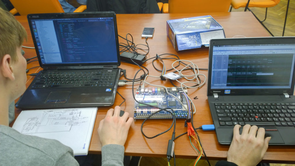
A hackathon at KPI by MIPSfpga was experimental in the sense that usually participants either simply program (for example, SaaS solutions) in hackathons, or make devices from ready-made fixed circuits and program them (Arduino, STM32 Discovery). Here, the participants wrote the program and developed the scheme, the interface unit at the Register Transfer Level (RTL), and then embedded this unit into the synthesized system with the MIPS microAptiv UP processor core and the AHB-Lite bus, and implemented this system in FPGA.
')
This is how it looked on the screens of their laptops, on the FPGA board and conceptually:

Such exercises will help grow systems engineers who are familiar with the development of circuitry and programming, which is necessary in the 21st century, the era of system-on-chip (SoC). It is also a way to prototype ASIC (Application Specific Integrated Circuits) prototyping, such as those found in various embedded systems, from coffee makers to satellites. Then, Ukrainian researchers at the KPI and KNU will be able to work with the European service Europractice and produce experienced chips in the factory via the MPW shuttle . If at the same time, researchers come up with something commercially interesting, they can use such a prototype to attract venture capital and create startups in certain niches, such as the niche of smart sensors for the Internet of things .

Before the hackathon on MIPSfpga, there were three days of Nanometer ASIC workshops and lectures on MIPSfpga . More than a hundred people signed up for Nanometer ASIC and more than eighty came:
Quite a few people also came to the lecture part about MIPSfpga, and the survey revealed that Verilog owns quite a lot of them, as well as knowledge about architecture and microarchitecture:
The most purposeful remained on the hackathon:
From the Facebook key organizer of the hakaton ( Wіdkrita laboratories elektronіki Lampa KPI ):

And one more command:
View 50 photos from Nanometer ASIC and MIPSfpga in Kiev
Now let's talk about the technical part.
A few words for those readers who are not familiar with what Verilog, ASIC and FPGA are:
From a post on Geektimes “ Armsmen of microelectronics. Video report from the San Francisco Electronics Design Conference :
From the post on Habrahabr How to start developing iron using FPGA - step by step instructions :
If you want to study such material from scratch, you can download Harris & Harris , an extremely popular tutorial, which Russian translation was translated by the British site Imagination twice ( first time , second time ) for free.
If the tutorial is too big for you and you just want to quickly understand the basic concepts, you can download a set of slides (also for free) that help teachers give Harris & Harris lectures . These slides are an addition to the textbook, they are also effective for self-education and quick introduction to the subject.
And finally, according to the wishes of the readers, in addition to the free electronic version of Harris & Harris, a paper version of Harris & Harris will be released on New Year's Eve , though not free (cellulose is more expensive than electrons):

True Harris-and-Harris helps mainly if you want to study the front-end (that is, the logical design of digital circuits and micro-architecture). If you want to get an educational program on the physical part of the design and production, then you can download the translation into Russian of Charles Danchek’s slides .
In addition, eNANO (a daughter of RUSNANO for educational programs) is going to add a video of Charles Danchek's lectures (with simultaneous translation into Russian) here in this directory :

But back to the hackathon in the KPI:
The main organizers of the hackathon were the Department of Designing Electronic-Computing Equipment of the Faculty of Electronics of the KPI, Vidkrit Laboratory of Electronic Electronics Lampa KPI , Students' Prost. Belka and the Department of Computer Engineering of the Faculty of Radio Physics, Electronics and Computer Systems of Taras Shevchenko National University of Kyiv.
In the photo on the left is Alexander Barabanov , an associate professor at Kiev University, he translated part of Harris & Harris, as well as a significant part of materials on MIPSfpga, Nanometer ASIC and Connected MCU into Russian. Right: Yevgeny Korotky , Head of the KPI Lamp:

As an example, the hackathon participants were shown the code for the integration of the light sensor - Digilent PmodALS - Ambient Light Sensor . Here is the sensor:

The sensor uses the SPI serial protocol for data transmission. The protocol variant used by the sensor is fairly simple; Its description in the documentation from the site of the manufacturer Digilent takes only two paragraphs of text:
Note that the Sensor Protocol (SPI) is serial, and the processor bus protocol (AHB-Lite) is parallel. Compare:
Using the SPI protocol, data is transmitted and received, bit by bit. This saves the number of signals, which is important for protocols transferring data between chips:

Using the AHB-Lite protocol, data bits are transmitted in parallel. In addition, the data in this protocol is associated with the address, and the address bits are also transmitted in parallel. Here are the diagrams for some of the read and write transaction signals on the AHB-Lite bus:
Reading:

Record:

To integrate the sensor into the system, you need to design three components:
The code on the chain for the hardware module that receives data using the SPI protocol and stores it in the current value register:

Here is the scheme for this code during logical synthesis using Altera Quartus II version 16.0 (after analysis, but before mapping and optimization):

The MIPSfpga hackathon turned out to be an even more interesting event for all participating than expected:
Therefore, there is an idea to repeat such a Hackathon in other countries. For repetition in Russia: in Moscow there are 16 Altera / Terasic DE0-CV boards that can be used for such events. In Kazakhstan and Ukraine, you can also come up with something. If you have ideas, please report in the comments.

A hackathon at KPI by MIPSfpga was experimental in the sense that usually participants either simply program (for example, SaaS solutions) in hackathons, or make devices from ready-made fixed circuits and program them (Arduino, STM32 Discovery). Here, the participants wrote the program and developed the scheme, the interface unit at the Register Transfer Level (RTL), and then embedded this unit into the synthesized system with the MIPS microAptiv UP processor core and the AHB-Lite bus, and implemented this system in FPGA.
')
This is how it looked on the screens of their laptops, on the FPGA board and conceptually:
Why do we need such tasks?
Such exercises will help grow systems engineers who are familiar with the development of circuitry and programming, which is necessary in the 21st century, the era of system-on-chip (SoC). It is also a way to prototype ASIC (Application Specific Integrated Circuits) prototyping, such as those found in various embedded systems, from coffee makers to satellites. Then, Ukrainian researchers at the KPI and KNU will be able to work with the European service Europractice and produce experienced chips in the factory via the MPW shuttle . If at the same time, researchers come up with something commercially interesting, they can use such a prototype to attract venture capital and create startups in certain niches, such as the niche of smart sensors for the Internet of things .
Photos and videos from hakaton
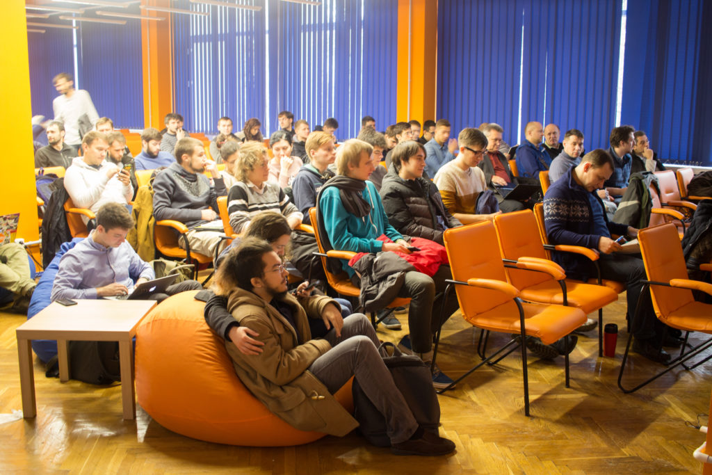
Before the hackathon on MIPSfpga, there were three days of Nanometer ASIC workshops and lectures on MIPSfpga . More than a hundred people signed up for Nanometer ASIC and more than eighty came:
Quite a few people also came to the lecture part about MIPSfpga, and the survey revealed that Verilog owns quite a lot of them, as well as knowledge about architecture and microarchitecture:
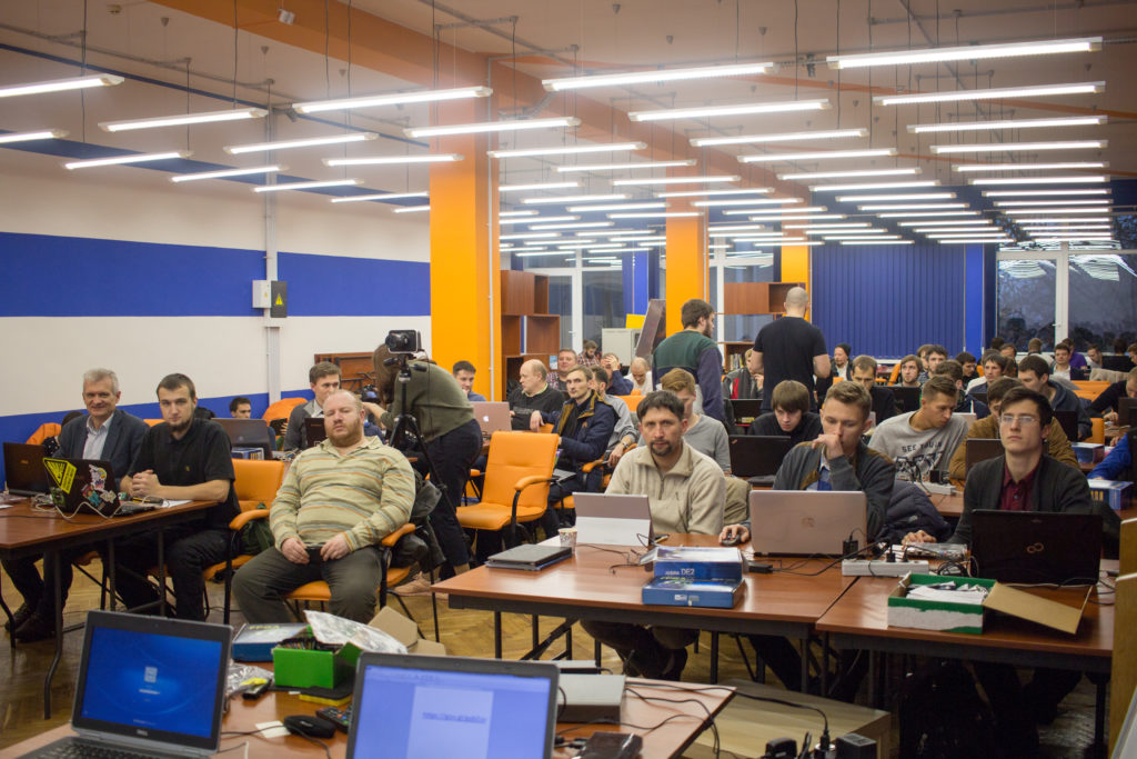
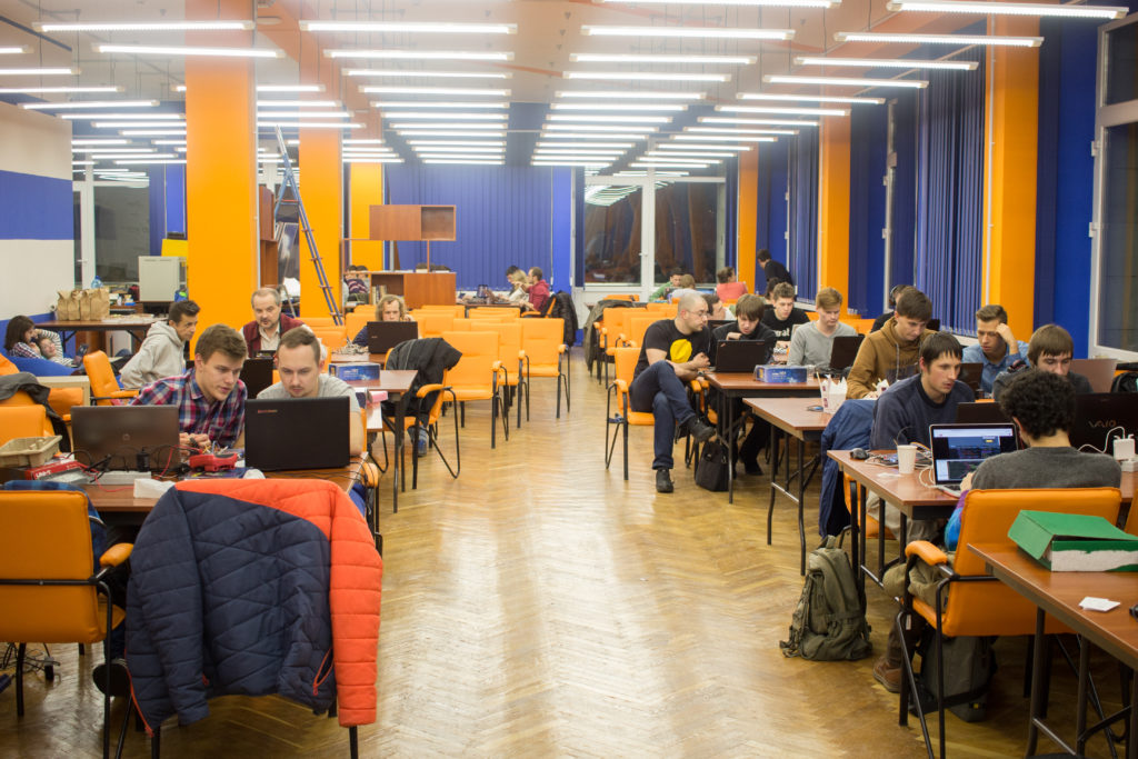
The most purposeful remained on the hackathon:
From the Facebook key organizer of the hakaton ( Wіdkrita laboratories elektronіki Lampa KPI ):
... In the meantime, here's a video with one of the winners, Denis Soldatov, who first completed the development of the device and received a DE0-CV fee and a proprietary MIPSfpga flash drive.
Denis has integrated the ultrasonic rangefinder from Digilent (https://goo.gl/Txoxl6) into the MIPSfpga system-on-chip. I wrote an interface module on Verilog that works with the sensor via hardware uart and has control registers mapped into the MIPSfpga address space via the AMBA bus. Denis also wrote a control program that reads the sensor from the registers mentioned above and, when the threshold is exceeded, beeps a certain frequency. ...
Fotochki with another team of winners!
Sergey Sachov and Valera Marchenko have integrated the keyboard from Digilent into the system-on-chip MIPSfpga (https://goo.gl/Xmbba6). The guys wrote on Verilog an interface module that works with a keyboard on a 16-pin interface and has a register containing the key code that is mapped to the MIPSfpga address space via the AMBA bus. A control program was also written, which reads the code of the pressed key from the mentioned register and displays the corresponding key number on a seven-segment indicator.
And one more command:
View 50 photos from Nanometer ASIC and MIPSfpga in Kiev
Now let's talk about the technical part.
Preliminary clarifications to the technical part
A few words for those readers who are not familiar with what Verilog, ASIC and FPGA are:
From a post on Geektimes “ Armsmen of microelectronics. Video report from the San Francisco Electronics Design Conference :
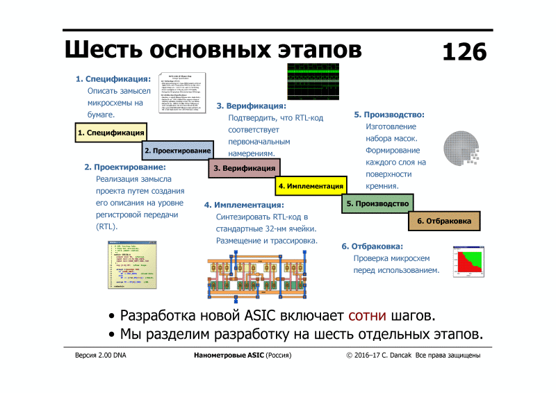
So far we have discussed the culmination of the microelectronic project - the manufacture of microchips in the factory. But how does such a project start?
In the past 25 years, chip design has most often been written in the Verilog hardware description language ([previously] in Europe and among the military - VHDL), after which a special program (logic synthesis) turns the design into a graph of wires and logical primitives, another program (static timing analysis) informs the designer whether it fits into the speed budget, and the third program (place-and-route) lays out this design on the chip site.
When the design goes through all the stages: coding on the chain, debugging, verification, synthesis, static timing analysis, floorplanning, place-n-route, parasitics extraction, etc. - it turns out a file called GDSII, which is sent to the factory, and the factory bakes chips. The most famous factories of this type are owned by Taiwan Semiconductor Manufacturing Company or TSMC.
From the post on Habrahabr How to start developing iron using FPGA - step by step instructions :
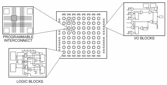
In its simplest form, an FPGA consists of a matrix of homogeneous cells, each function of which can be changed using multiplexers connected to the bits of the configuration memory. One cell can become AND gate with four inputs and one output, the other one single-bit register, etc. We load into the configuration memory a sequence of bits from the memory — and a predetermined electronic circuit is formed in the FPGA, which can be a processor, a display controller, etc.
FPGAs / FPGAs are not processors, “programming” the FPGAs (filling in the FPGA configuration memory) you create an electronic circuit (hardware), while programming a processor (fixed hardware) you slip a chain of sequential instructions written into the memory (software).
If you want to study such material from scratch, you can download Harris & Harris , an extremely popular tutorial, which Russian translation was translated by the British site Imagination twice ( first time , second time ) for free.
If the tutorial is too big for you and you just want to quickly understand the basic concepts, you can download a set of slides (also for free) that help teachers give Harris & Harris lectures . These slides are an addition to the textbook, they are also effective for self-education and quick introduction to the subject.
And finally, according to the wishes of the readers, in addition to the free electronic version of Harris & Harris, a paper version of Harris & Harris will be released on New Year's Eve , though not free (cellulose is more expensive than electrons):
True Harris-and-Harris helps mainly if you want to study the front-end (that is, the logical design of digital circuits and micro-architecture). If you want to get an educational program on the physical part of the design and production, then you can download the translation into Russian of Charles Danchek’s slides .
In addition, eNANO (a daughter of RUSNANO for educational programs) is going to add a video of Charles Danchek's lectures (with simultaneous translation into Russian) here in this directory :
But back to the hackathon in the KPI:
Hackathon organization
The main organizers of the hackathon were the Department of Designing Electronic-Computing Equipment of the Faculty of Electronics of the KPI, Vidkrit Laboratory of Electronic Electronics Lampa KPI , Students' Prost. Belka and the Department of Computer Engineering of the Faculty of Radio Physics, Electronics and Computer Systems of Taras Shevchenko National University of Kyiv.
In the photo on the left is Alexander Barabanov , an associate professor at Kiev University, he translated part of Harris & Harris, as well as a significant part of materials on MIPSfpga, Nanometer ASIC and Connected MCU into Russian. Right: Yevgeny Korotky , Head of the KPI Lamp:
On the eve of the hackathon, Yevgeny Korotky sent out the following letter:
Shanovі participants hakatonu, privіt!
They were familiarized with the MIPSfpga and the transfer of the perimeter for innovation.
Kіlka organіzatsіynykh moments.
Task hakatonu.
It is necessary to integrate peripheral attachment to the system on the basis of MIPSfpga. Іntegratsіya poligaє u v_dobrazhennі regіstrіv perferіynogo pristroyu in address protіr MIPSfpga. You must write on Verilog / VHDL a first module, one that hangs on AHB-Lite, another one, one reg is set, another one is attached and one is synchronized with another one. Well, and Vikonuvaty Obnіn Dani i attachment attachment protocol. Also, a program for MIPSfpga will be required, and it will be shown to the robot with the perimeter attachments.
On the changes of the peripherals:
https://docs.google.com/spreadsheets/d/1djURILzdHSwnvxC5SzO4izU2imyimAgjOuXXAef6-rQ/edit?usp=sharing
However, they did not interfere only with the integration of the peripherals. It’s right to win a ounce of your dreams of projects on the basis of MIPSfpga, above them on qiu to your address.
Commands
We will have 14 FPGA cards for the MIPSfpga port (9 DE2 boards, 1 DE1 board, 4 DE0-CV boards). A maximum of 14 teams is possible. You can bring your fpga fee for transferring it is quiet, for the port of MIPSfpga (transfer here:
https://github.com/MIPSfpga/mipsfpga-plus/tree/master/boards ), but I have to pay the fpga fee (for example, you can learn more about portuvati on MIPSfpga and MEPSfpga nets, with a plus plus);
You can already form a team. Peripherals List for Integration Issues for Reagents:
https://docs.google.com/spreadsheets/d/1djURILzdHSwnvxC5SzO4izU2imyimAgjOuXXAef6-rQ/edit?usp=sharing
Scrap yourself up to the commanding team of the integration of singing in your own name in the “Team” command. At the beginning of the game, in the commands of the participants, enter the rules through whom. Lyudyna Yak will become the first commandant captain. Your uvashu zvertaєmo, scho have google table all the history of redaguvannya available.
Timelines hakatonu.
Coming on the 8th wound. During the day, we’ll have two reviews and two mentor sessions, and we’ll assess the progress (the mentor sessions will be clarified with trochies, because these are not principle principles). Also, during the day, you can assign power to the mentors (Yuri Panchul, Short Yevgen) for a digital design, MIPSfpga and a new program.
Presentations of projectors begin about the 20th year.
The presentation is a demonstration of a robot attachment, prowed by a scoop of information, just like that. For presentation you can use a projector. In the presentations and demonstrations, the fate of many people will be accepted. The triviality of the present is 3 hvilini. About 20-45 completed presentation. At about 21-00, obscenely restarted and distribute to all participants.
Prize
The top prize is the Altera DE0-CV board with numbers quietly scattered from the hackathon. It’s not possible to increase the size of the project, we will give two paychecks to the teams. Zvarnit respect, head of the prize to give commands. Yak vi yogo dіlitimete - at your factory. Also, participants should write down the coaxial prizi about yaki vi dіzna be the first hour of the harvest. One way you can tell - the stench will surely be to you.
Eh
With a hackathon, you will be able to move on. I like it in Noodle Doodle:
https://eda.ua/restorany/lapsha-bar-noodle-doodle?gclid=CjwKEAiAr4vBBRCG36e415-_l1wSJAAatjJZgqN6K9uVvj4_XnQRioEBzgScrYK6BNi0lZb-HZH
I think you have pobabannya on grasses, you can over Dmitri
( https://vk.com/im?sel=75362095 ) until evening. You can turn one thing on the skin with two priyomіv їі.
Until zustrіchі on hakatonі)
- 3
Organizer call


Example for participants - light sensor
As an example, the hackathon participants were shown the code for the integration of the light sensor - Digilent PmodALS - Ambient Light Sensor . Here is the sensor:
The sensor uses the SPI serial protocol for data transmission. The protocol variant used by the sensor is fairly simple; Its description in the documentation from the site of the manufacturer Digilent takes only two paragraphs of text:


Note that the Sensor Protocol (SPI) is serial, and the processor bus protocol (AHB-Lite) is parallel. Compare:
Using the SPI protocol, data is transmitted and received, bit by bit. This saves the number of signals, which is important for protocols transferring data between chips:
Using the AHB-Lite protocol, data bits are transmitted in parallel. In addition, the data in this protocol is associated with the address, and the address bits are also transmitted in parallel. Here are the diagrams for some of the read and write transaction signals on the AHB-Lite bus:
Reading:
Record:
To integrate the sensor into the system, you need to design three components:
- A hardware module that receives data using the SPI protocol and stores it in some register of the current value. The code on the verification for this module is in the file , as well as below.
- The code on the chain for transferring data from this register over the AHB-Lite bus to the processor core for data processing by software, so to speak glue code. It can be found in the directory files , if you search the string `ifdef MFP_DEMO_LIGHT_SENSOR. .
- Software running on a processor core that receives data from the light sensor and somehow uses it, for example, displays the light value on a 7-segment display on the FPGA board. This is a small C program that is compiled using the standard GCC toolchain and linked with initialization code written in assembly language - see here .
The code on the chain for the hardware module that receives data using the SPI protocol and stores it in the current value register:
Here is the scheme for this code during logical synthesis using Altera Quartus II version 16.0 (after analysis, but before mapping and optimization):
Conclusions and future plans
The MIPSfpga hackathon turned out to be an even more interesting event for all participating than expected:
- Hackathon was not very easy - not all came to the finish line, but less than half of the teams
- Hackathon was not very difficult - two teams came confidently, another one or two - with some stretch
- In the process of the hackathon, the participants made a bunch of mistakes for both beginners and more advanced developers, in particular:
- Newbie Trivial Error: Misinterpreting I / Os
- Misunderstanding of the mechanism of Verilog operation: Shift by clock cycle due to misunderstanding of the concept of delta cycles and waiting for an immediate change of the external signal inside the always- combinational block in response to assignment to the signal on which the external signal depends on continuous assignment
- Misunderstanding of the Register Transfer Level Methodology (RTL): use of control signals in “always @ (posedge control_signal) ...” instead of “always @ (posedge clock) ... if (control_signal) ...”
- Wrong timing constraints
- Found even an error in the code of the MIPSfpga package!
Therefore, there is an idea to repeat such a Hackathon in other countries. For repetition in Russia: in Moscow there are 16 Altera / Terasic DE0-CV boards that can be used for such events. In Kazakhstan and Ukraine, you can also come up with something. If you have ideas, please report in the comments.
Source: https://habr.com/ru/post/316248/
All Articles