Acquaintance and start of development on iCE40 FPGAs from Lattice Semiconductor
 Hello! Today we will get acquainted with the new family of cheap and low-power FPGAs from Lattice Semiconductor iCE40LP / HX / LM families, learn how to work with the proprietary compiler iCEcube2 and the Sublime Text 3 code editor, and also program the chip on the Lattice iCEstick debug board using firmware written in SystemVerilog.
Everything will be accompanied by detailed instructions and screenshots.
It happens that microcontrollers are not suitable for some tasks in the development of iron, especially those associated with high parallelism of data processing, speed of processing or with other specifics of the task, and something powerful from Cortex-A is seen as a sparrow cannon. Then, as a rule, the developer draws attention to the FPGAs, providing for a relatively inexpensive price to him full freedom of action at the lowest level of digital systems - individual logic elements and triggers. This allows you to make "your own chip" inside the FPGA, using its findings and the periphery already embedded inside. For example, if you suddenly need 50 timers with PWM, or ultra-fast data processing, or, say, SPI with 3 MISO lines and 2 MOSI, transfer 5 Gbps with 2 diff. lines - all this is quite realizable on the FPGA. The engineer here is limited only by the number of universal logical cells and their switching time.
Among the FPGA manufacturers, two have already gained popularity among developers - Altera and Xilinx, which produce both the simplest FPGAs (MAX II, MAX 10, Spartan II, Spartan III), on which you can build logic of almost any complexity, as well as ultrafast (Stratix 10, Arria 10, Spartan 7, Artix 7), capable of transmitting data at speeds up to 56 Gbps, so that you have fast internet. However, such dreadful speeds of work are not always needed.
')
Some features of the FPGA of the iCE40 family (data from the manufacturer’s website):
• Series HX - high-performance FPGAs, LP - low-power and LM - low-power with integrated peripherals;
• From 384 to 7680 LUT cells;
• Low power consumption, starting at 25 µW for some chips;
• Interfaces integrated into the SPI and I2C hardware, which facilitate the configuration of the chip;
• Ability to implement interfaces: Parallel RGB, 7: 1 LVDS, MIPI DPI / DBI, HiSPi, subLVDS, LVDS, Parallel LVCMOS;
• Up to 128 kbps of internal RAM;
• There is no internal flash memory, so you will need to connect external memory to the built-in automatic SPI interface (suitable models can be found in the Diamond Programmer firmware);
• BGA cases with 0.35-0.4 mm pitch, with minimum dimensions of 1.40x1.48x0.45 mm with 0.35 mm pitch, there is also a TQFP-144 package with a 0.4 mm pitch.
If Altera and Xilinx have comfortable development environments with a large number of lessons on them, then Lattice software is a compiler with a shell over Synopsys Synplify, and writing code there seemed to be inconvenient for me, so I decided to just load ready-made source files there. Software for other series - Lattice Diamond is not suitable for the iCE40 series, so for editing the code I put the well-known Sublime Text 3 editor and installed a plugin on it to support the SystemVerilog language. You can write in other languages, iCEcube2 automatically recognizes the language by file extension.
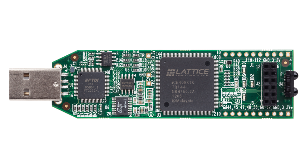
Well, if you have an iCEstick debug board with USB (clickable images from manufacturer sites):
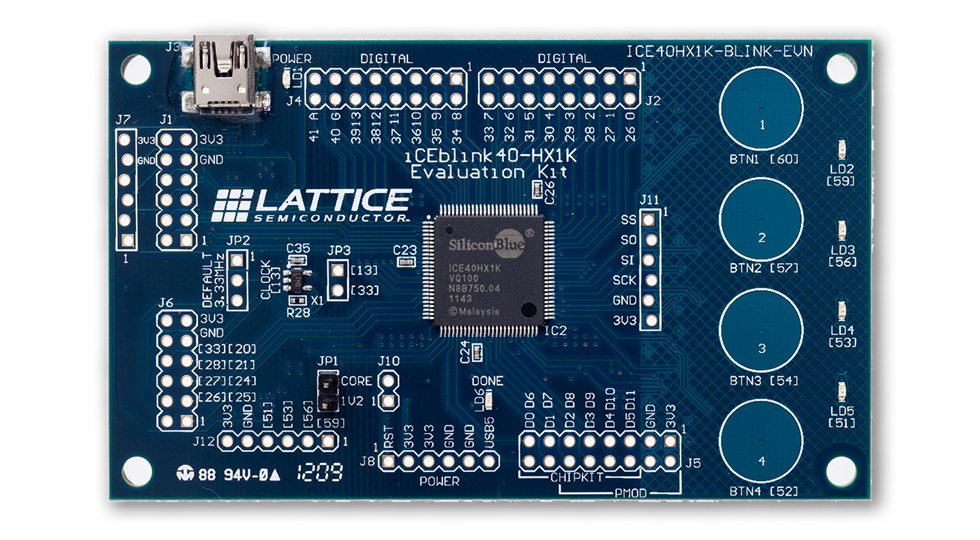
Instead, you can buy this one (pinout and firmware settings will be different!):
So, the detailed steps for installing the software, creating and configuring the project and the firmware, test code, firmware and monitoring the results:
1. Register on the Lattice Semiconductor website and download iCEcube2 .
2. Click “Click here to request your license” on the same page. After that, you will need to enter your MAC address in the field.
3. You will receive an email with a license file.
4. Install iCEcube2, copy the license file to its folder, and point the path to it by running iCEcube2.
5. Install the firmware for the FPGA firmware - Lattice Diamond Programmer .
6. Install Sublime Text 3 and the package manager for it .
7. In Sublime Text 3, click Preferences → Package Control, in the list that opens, click “Package Control: Install Package”.
8. Enter "SystemVerilog". Click on the first (and only) item in the list, wait until the plugin is installed (see the line at the bottom of the editor).
9. Create an empty file and save it as top.sv where the sources of your FPGA firmware project will be.
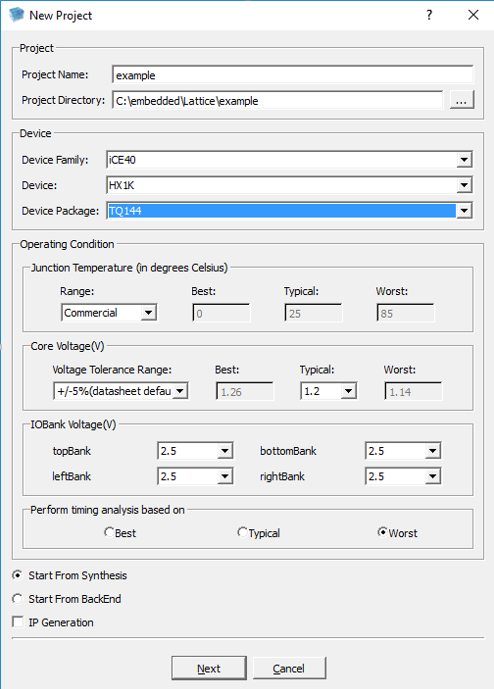
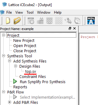
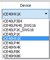
10. In iCEcube2, click the New project (or the yellow sheet at the top), a window will open where you need to fill in the parameters as in the screenshot, indicating the project path:
11. Click Next, a window will appear to add source files to the project, look for our file top.sv, double click on it and click Finish.
12. The project is created, on the left is its tree and the steps of synthesis, placement and tracing of connections between cells. Item Design Files is disclosed, there are all included in the project files. Now there is only top.sv:
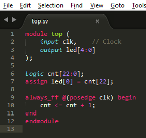
13. Let's write a standard code for flashing the LED (well, if you have an iCEStick board):
14. Save the changes in the file and go to iCEcube2. Click there on this file twice, and on the question of whether to update the file, answer "Yes".
15. In iCEcube2, click Tools> Run All and wait for the project to complete.
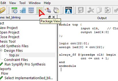
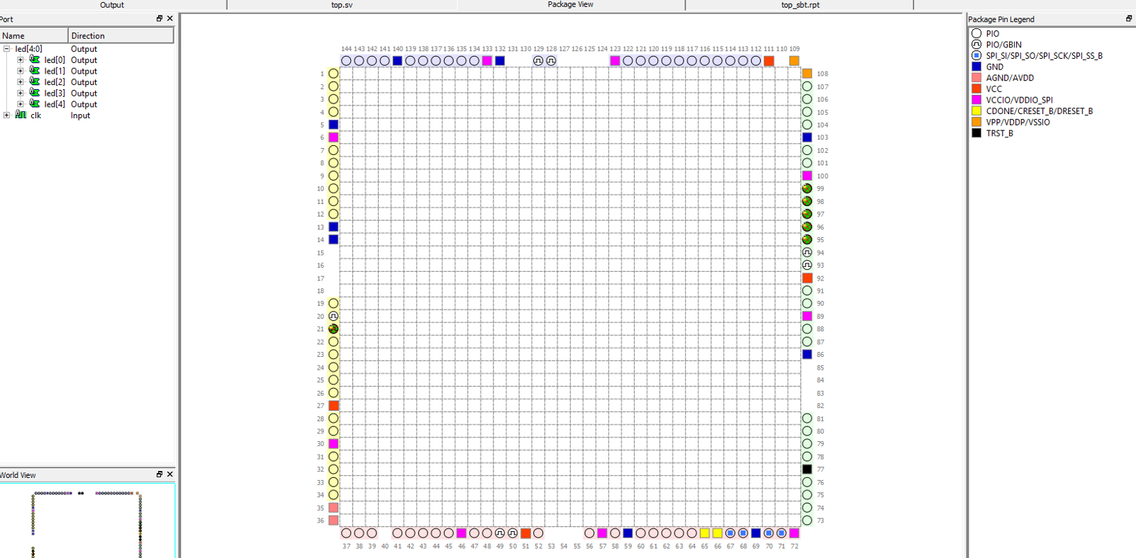
16. Click on the button with 16 green circles, Package View:
17. The pin editor opens in which you can correlate the inputs and outputs of your module to SystemVerilog and the FPGA body pins. The body layout can be scaled (Ctrl + rotate the mouse wheel) and moved (by dragging the cursor):
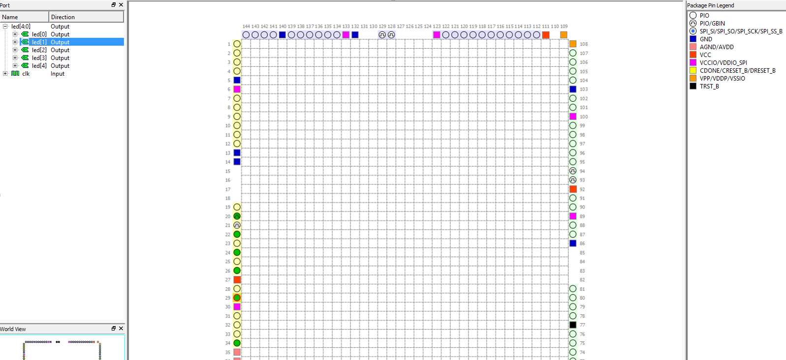
18. If you download the datasheet for debugging the iCEstick, you can find out that the clock generator is connected to 21 pins, and 5 LEDs to 95 (green), 96, 97, 98 and 99 (red) pins. In the panel on the left of the Port, you need to open the led [4: 0] bus, which we have brought instead of one output so that we will not blink iron 0 on those diodes, otherwise they will shine dimly. Now, with the mouse, drag all items led [0] .. led [4] to the leads to which the LEDs are connected, and clk to the leads to 21 leads.
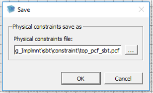
19. If done correctly, these findings on the diagram will turn green. After that, you need to click on each of them with the right button and click Lock in the drop-down menu, after which locks will appear on them. This will save you from resetting pinouts when recompiling code. Now save the pinout by pressing Ctrl-S. In the following windows, click OK and Yes:
20. Again, click on the 16 circles (Package view). The resulting picture looks like this:
21. Click Tools → Run All and wait for the full compilation of the project.
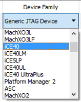
22. Insert the iCEstick debugging into the USB port of the PC and run the Diamond Programmer, click File> New File there. A window will open in which you can click Detect Cable, or you can manually select these parameters:

23. Click OK and wait for the scan:

24. If all is well, the line will appear:

If everything is bad, try another USB port.
25. Fill in the parameters:
26. In the Operation column, click on the Fast programming sign, a window opens:
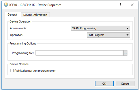
In which you need to select the SPI Flash Programming item in the Access Mode drop-down list, after which the window will increase, and now you need to fill in the remaining fields as in the screenshot:

27. Click OK, or Enter, as you prefer, and then save the firmware configuration by pressing Ctrl-S.
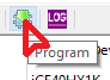
28. Click Program and wait a minute until the FPGA is erased and again programmed:

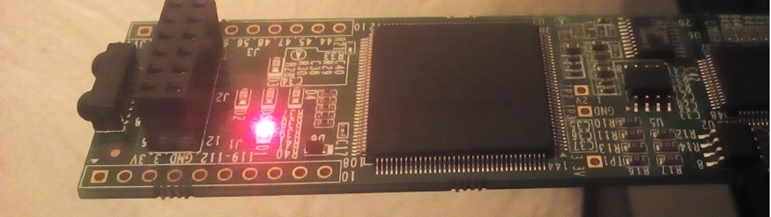
29. Observe the result: the red LED flashes with a noticeable frequency:

Conclusion
We learned how to set up and build a project with code in iCEcube2 software, set up the firmware and load the firmware into the FPGA chip. We wrote a test code for the flashing LED on the board and confirmed its operability.
In order to apply the FPGA of the iCE40 family in your projects you need to study the datasheets for the selected chip and its debug boards. The cheapest chip in the family, the ICE40UL640-SWG16ITR50, costs Digi-Key $ 1.53 / pc, has 640 cells, 55 kb of RAM, and a WLCSP-16 package with a size of 1.4x1.48 mm. The most expensive chip in the series - ICE40HX8K-CT256 costs 12.78 $ / pc in Digi-Key, has 7680 cells, 128 kb of RAM, and a BGA-256 package measuring 14x14 mm.
In further articles, a review will be conducted of similar manufacturers of FPGAs from other manufacturers and compared with iCE40 for price, speed, number of cells, variety of cases, availability in Russia, ease of use of the development environment, etc.
Source: https://habr.com/ru/post/315588/
All Articles