Thermal Resistance: Production Process
Among the ideally green Swiss meadows, next to the barn, is a modern minimalist building with panoramic windows. Here are the main office and main production facilities of the Swiss company IST-AG.
Most of the products manufactured by IST-AG are thin-film temperature sensors, also known as thermal resistance (RTD). From the article " Thermal Resistance: Theory " you can find out what it is and how it works.

')
Today I will talk about the main stages of the production process. Like semiconductor manufacturing, it all starts with a ceramic substrate.
Let me remind you that the thin-film sensor is a resistor made on the basis of platinum, nickel or copper.
The manufacturing technology of thin-film sensors originates in the semiconductor industry: a thin layer of metal is sprayed onto the ceramic substrate, from which a conductive path is formed, which is often called a meander. The metal meander is covered on top with an insulating (passivation) layer of glass that is resistant to temperature and chemical attack. Specially selected glass composition is also used to fix the findings.
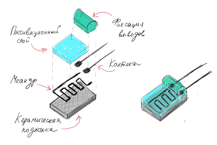
Thus, the first stage of production is the application of platinum on a ceramic substrate.
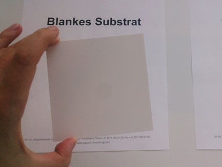
For temperature sensors, an alumina substrate (99.6% Al2O3) is used, but in the production of other thin-film sensors other materials can be used - sapphire, zirconium, polyimide, glass, silicon, etc.
The standard thickness of the ceramic substrate is 0.63 mm, but special sensors are sometimes made with a substrate 0.80 and even 0.25 mm thick. Reducing the thickness of the substrate can reduce the response time of the sensor, thin substrates are also used in the manufacture of sensors with high nominal resistance, for example 10 kOhm.
Ceramic plates are subjected to chemical cleaning and etching. Naturally, these operations are performed in a clean room with modern equipment. Two things need to be said about the clean room in IST: it is ISO-5 certified and there is a wonderful view of alpine meadows from there.
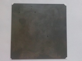
A layer of metal is sprayed onto the cleaned ceramic plate. The composition of the metal determines the type of dependence of the sensor resistance on the measured temperature - different types of platinum correspond to different coefficients A, B and C of the polynomial R (T), this is the previous article .
Platinum Spray Plate
A photoresist is applied to the cleaned ceramic plate - a photosensitive material that is used as a mask for the formation of conductive structures in the manufacture of semiconductors, in the production of printed circuit boards and in other processes. The photoresist is applied by centrifugation.
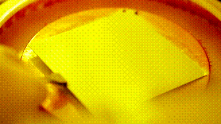
The photoresist is sensitive to the ultraviolet spectrum, so this stage of work is carried out with nonactinic (yellow) light.
Platinum coated with photoresist
The photoresist plate is combined with the mask, which determines the structure of the meander, and hence the important parameters of the future sensor - the nominal resistance R0 and size.

Next is the exposure - the plate with the superimposed mask lights up, thus the unclosed areas of the photoresist are fixed on the plate.

After etching — removing the photoresist from the unlit areas — conductive tracks remain on the ceramic plate.
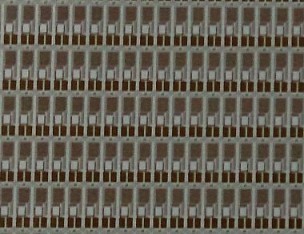
Depending on the mask used, a different number of sensors is placed on the plate, an average of about 2000 pieces. It is easy to guess that the use of the "unpopular" mask, that is, the manufacture of sensors with rare characteristics, is unprofitable for small orders.
At the same production stage, metal plates are applied to the plate for fastening the leads; for this purpose, screen printing is used.
The geometry of the meander applied to one of the standard masks can be corrected using a laser fit. The last article mentioned the fact that in addition to the standard R0 - 50, 100, 500, 1000 Ohms, thermal resistance can have a nominal resistance, shifted relative to the standard value. Shift R0 can be done just due to the laser fit.
After the meander is formed, the plate is covered with a passivation layer of glass. Next, the plate is cut, and the sensor blanks are moved from the clean room to the usual room.

When the plates are cut, pins are added to the sensors — automatic machines weld the pins onto the contact pads, after which the fixing point is covered with a protective layer of glass.

This completes the production of sensors. Further procedures are carried out to verify the accuracy of each item and product packaging.
The accuracy check reveals to which tolerance class (here again I refer to the previous article ) each element corresponds. At a very rough estimate, about one third of the sensors of each class (B, A, AA) are obtained from each plate. Hence the price difference — class B is the cheapest, a similar class A sensor will cost 20 percent more, and a class AA sensor another 20-30 more expensive — the most accurate sensors undergo additional control measurements.
Let's return to the conclusions of the sensors. Findings are made of different materials, may have different lengths and shapes (round / flat). Sensors with stranded leads, sensors with enameled and insulated leads are available. Most sensors have two outputs, but there are also elements for 3- and 4-wire switching circuits.
The type of terminals depends primarily on the temperature range of the sensor. For example, enameled copper wires tolerate only temperatures up to + 150 ° C, conclusions from silver and nickel alloys withstand higher temperatures. For temperatures up to + 600 ° C, wires with platinum coating are required, and for work with temperatures up to +750 or up to + 850 ° C, all platinum leads are needed.

By the way about the length of the findings. Most often, if the sensor needs long leads, then the contacts are expanded to the desired length - the additional wire is welded or soldered. However, there are tasks in which the requirements for reliability are so high that an additional connection is unacceptable and the conclusions of the required length must be established initially. Thus, in the manufacture of sensors for CERN, pins as long as 35 meters were welded to the contact pads of the sensor.
Most resistance thermometers are output components, but it is precisely thanks to thin-film technology that thermal resistances for surface mounting have appeared (I’m not tired of referring to the previous article ).
Available as a classic SMD-components, and sensors for mounting Flip-Chip. Flip-Chip components require more sophisticated equipment (precise positioning, Z-force control, extra dust protection). On the other hand, Flip-Chip sensors are cheaper, they take up less space, and in general the future is behind them.

Surface mount sensors are available in standard sizes - 1206, 0805 and 0603.
Generally speaking, the diversity of buildings is one of the main features of IST. Here they make a variety of sensors, and non-standard solutions are available not only for large customers, but also for medium-sized industries.
For example, for direct replacement of winding sensors with thin-film sensors, thermal resistances are produced in a special cylindrical housing. A miniature rectangular sensor fits inside a ceramic case that repeats the classic winding sensor form factor.

Such a case does not perform any protective functions, its only meaning is a smooth transition from winding thermo-resistance to thin-film ones.
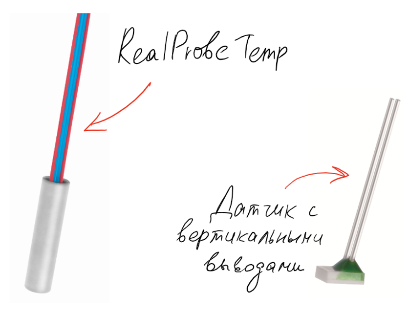
Thermal resistors are very popular, they are made in the form of probes - stainless steel sleeves, which are lowered into a liquid medium. Typically, such sensors are made as follows: the sensitive element - a thin-film or winding sensor - is placed in a metal case, after which the sleeve is filled with something like magnesium oxide (high thermal conductivity plus good electrically insulating properties).
When using thin-film technology, this design can be improved: since thin-film sensors are flat and relatively small in size, the sensor can be mounted directly on the “bottom” of the sleeve.
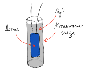
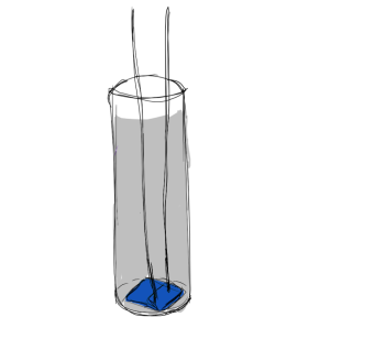
Thus, two positive effects are achieved. First, the response time is significantly reduced (the sensor goes into operating mode in less than one and a half seconds). Secondly, the sleeve can be lowered into the measured medium not completely, but by only 10 mm with almost no loss of accuracy.
Sensors made in this way are produced under the name RealProbeTemp [ datasheet ].
In the manufacture of RealProbeTemp sensitive elements are used, in which the pins are attached not in a standard way, but perpendicular to the sensor plane. Such elements are available separately, they are used in tasks when the sensor must be installed in a narrow hole or in a tube.
The fact that thin-film sensors are flat allows you to produce various special solutions for the best contact with the surface of the measurement object. In order to shorten the response time and ensure maximum accuracy of measurements, the back side is metalized at the sensor itself. Metallized sensors are available to order separately, but more often they are made immediately fixed on the contact pad. Contact pads can have various shapes and sizes, depending on the task.
For example, for better contact when measuring the temperature of a pipe, a flexible platform is needed, and when measuring the temperature of a small part, it is easier to take a separate sensor and attach it to the part itself.
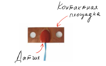
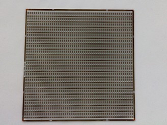
Several sensors with contact pads can also be seen in the photo above .
In total, over the course of its history, IST released more than 4,000 different models of sensors and mostly platinum temperature sensors. Most of the company's production facilities are located in Switzerland, but some of the least technological operations are performed in a factory in the Czech Republic. Of course, this situation suggests the idea of the high cost of IST sensors.
Prices for IST thermistors are indeed higher than prices for similar noname solutions from China, but such a comparison is not in itself correct. Thermal resistors IST are certain guarantees of quality and reliability. There are many tasks where such guarantees are more important than the minimum price. To talk about quality and reliability is not unfounded, I note that the temperature sensor from IST, for example, flew the "Rosette" to the comet Churyumov-Gerasimenko.
At the same time, it’s difficult to call the prices for Swiss thermal resistances space - Pt100 class A in the SMD package I give from a warehouse in the Russian Federation for 2 euros per thing, Pt100 for class B in Flip-Chip cases at 0.98 euros, and the prices for output sensors for temperatures from -200 to + 300 ° C start at 3.68 euros. This is a retail with VAT, if that.
Concluding the story about the production of IST-AG, I add the proof of the neighborhood of IST headquarters with the barn. Thanks for attention.


In conclusion, I traditionally thank the reader for his attention and remind you that questions about the use of products, about which we write on Habré, can also be asked by email, specified in my profile.
upd: all mentioned sensors and modules are available from stock. More information on efo-sensor.ru
Most of the products manufactured by IST-AG are thin-film temperature sensors, also known as thermal resistance (RTD). From the article " Thermal Resistance: Theory " you can find out what it is and how it works.
')
Today I will talk about the main stages of the production process. Like semiconductor manufacturing, it all starts with a ceramic substrate.
Typical structure of a thin film sensor
Let me remind you that the thin-film sensor is a resistor made on the basis of platinum, nickel or copper.
The manufacturing technology of thin-film sensors originates in the semiconductor industry: a thin layer of metal is sprayed onto the ceramic substrate, from which a conductive path is formed, which is often called a meander. The metal meander is covered on top with an insulating (passivation) layer of glass that is resistant to temperature and chemical attack. Specially selected glass composition is also used to fix the findings.
Manufacturing process
Thus, the first stage of production is the application of platinum on a ceramic substrate.
Hereinafter I will talk about the production of platinum sensors. Firstly, the overwhelming majority of modern thermistors are platinum elements with a characteristic of 3850 ppm / K (this issue is discussed in more detail in the previous article ), and secondly, the production of nickel and copper thermistors is not much different.
For temperature sensors, an alumina substrate (99.6% Al2O3) is used, but in the production of other thin-film sensors other materials can be used - sapphire, zirconium, polyimide, glass, silicon, etc.
The standard thickness of the ceramic substrate is 0.63 mm, but special sensors are sometimes made with a substrate 0.80 and even 0.25 mm thick. Reducing the thickness of the substrate can reduce the response time of the sensor, thin substrates are also used in the manufacture of sensors with high nominal resistance, for example 10 kOhm.
Ceramic plates are subjected to chemical cleaning and etching. Naturally, these operations are performed in a clean room with modern equipment. Two things need to be said about the clean room in IST: it is ISO-5 certified and there is a wonderful view of alpine meadows from there.
A layer of metal is sprayed onto the cleaned ceramic plate. The composition of the metal determines the type of dependence of the sensor resistance on the measured temperature - different types of platinum correspond to different coefficients A, B and C of the polynomial R (T), this is the previous article .
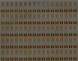
Platinum Spray Plate
A photoresist is applied to the cleaned ceramic plate - a photosensitive material that is used as a mask for the formation of conductive structures in the manufacture of semiconductors, in the production of printed circuit boards and in other processes. The photoresist is applied by centrifugation.
The photoresist is sensitive to the ultraviolet spectrum, so this stage of work is carried out with nonactinic (yellow) light.
Platinum coated with photoresist
The photoresist plate is combined with the mask, which determines the structure of the meander, and hence the important parameters of the future sensor - the nominal resistance R0 and size.
Next is the exposure - the plate with the superimposed mask lights up, thus the unclosed areas of the photoresist are fixed on the plate.
After etching — removing the photoresist from the unlit areas — conductive tracks remain on the ceramic plate.
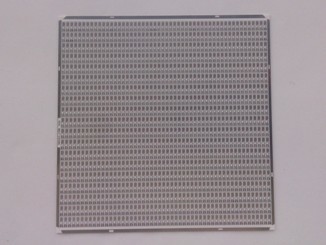
Depending on the mask used, a different number of sensors is placed on the plate, an average of about 2000 pieces. It is easy to guess that the use of the "unpopular" mask, that is, the manufacture of sensors with rare characteristics, is unprofitable for small orders.
At the same production stage, metal plates are applied to the plate for fastening the leads; for this purpose, screen printing is used.
The geometry of the meander applied to one of the standard masks can be corrected using a laser fit. The last article mentioned the fact that in addition to the standard R0 - 50, 100, 500, 1000 Ohms, thermal resistance can have a nominal resistance, shifted relative to the standard value. Shift R0 can be done just due to the laser fit.
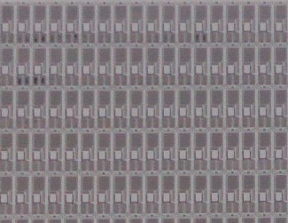
After the meander is formed, the plate is covered with a passivation layer of glass. Next, the plate is cut, and the sensor blanks are moved from the clean room to the usual room.
Here you can trace the interesting relationship between the size of the sensor and its price. There are about 15 standard dimensions of output sensors: 1.6 × 1.2 mm, 2 × 2 mm, 2.3 × 2 mm, 2.5 × 1.6 mm, 3 × 0.8 mm, 3 × 2.5 mm, 4 × 2 mm, 5 × 5 mm, 5 × 1.6 mm, 5 × 2 mm, 5 × 2.5 mm, 5 × 3.8 mm, 10 × 2 mm, etc.
It is logical that, other things being equal, the largest sensors in area will be more expensive - they require more materials for their production. However, there is another circumstance - sensors smaller than two millimeters are also more expensive, this is due to the method of cutting plates.
In most cases, to divide the plates into separate sensors, breaking is used, but for relatively small sensors this method is not applicable, therefore, in the manufacture of miniature sensors, the risks are first applied to the plate with a diamond cutter. Excess operation - additional cost. Thus, price sensors with dimensions of 2 x 2, 2.3 × 2 or 5 × 2 mm are optimal.
When the plates are cut, pins are added to the sensors — automatic machines weld the pins onto the contact pads, after which the fixing point is covered with a protective layer of glass.
This completes the production of sensors. Further procedures are carried out to verify the accuracy of each item and product packaging.
The accuracy check reveals to which tolerance class (here again I refer to the previous article ) each element corresponds. At a very rough estimate, about one third of the sensors of each class (B, A, AA) are obtained from each plate. Hence the price difference — class B is the cheapest, a similar class A sensor will cost 20 percent more, and a class AA sensor another 20-30 more expensive — the most accurate sensors undergo additional control measurements.
About output sensors
Let's return to the conclusions of the sensors. Findings are made of different materials, may have different lengths and shapes (round / flat). Sensors with stranded leads, sensors with enameled and insulated leads are available. Most sensors have two outputs, but there are also elements for 3- and 4-wire switching circuits.
The type of terminals depends primarily on the temperature range of the sensor. For example, enameled copper wires tolerate only temperatures up to + 150 ° C, conclusions from silver and nickel alloys withstand higher temperatures. For temperatures up to + 600 ° C, wires with platinum coating are required, and for work with temperatures up to +750 or up to + 850 ° C, all platinum leads are needed.
By the way about the length of the findings. Most often, if the sensor needs long leads, then the contacts are expanded to the desired length - the additional wire is welded or soldered. However, there are tasks in which the requirements for reliability are so high that an additional connection is unacceptable and the conclusions of the required length must be established initially. Thus, in the manufacture of sensors for CERN, pins as long as 35 meters were welded to the contact pads of the sensor.
About SMD sensors
Most resistance thermometers are output components, but it is precisely thanks to thin-film technology that thermal resistances for surface mounting have appeared (I’m not tired of referring to the previous article ).
Available as a classic SMD-components, and sensors for mounting Flip-Chip. Flip-Chip components require more sophisticated equipment (precise positioning, Z-force control, extra dust protection). On the other hand, Flip-Chip sensors are cheaper, they take up less space, and in general the future is behind them.
Surface mount sensors are available in standard sizes - 1206, 0805 and 0603.
Special enclosures
Generally speaking, the diversity of buildings is one of the main features of IST. Here they make a variety of sensors, and non-standard solutions are available not only for large customers, but also for medium-sized industries.
Replacing winding sensors
For example, for direct replacement of winding sensors with thin-film sensors, thermal resistances are produced in a special cylindrical housing. A miniature rectangular sensor fits inside a ceramic case that repeats the classic winding sensor form factor.
Such a case does not perform any protective functions, its only meaning is a smooth transition from winding thermo-resistance to thin-film ones.
Metal sleeves
Thermal resistors are very popular, they are made in the form of probes - stainless steel sleeves, which are lowered into a liquid medium. Typically, such sensors are made as follows: the sensitive element - a thin-film or winding sensor - is placed in a metal case, after which the sleeve is filled with something like magnesium oxide (high thermal conductivity plus good electrically insulating properties).
When using thin-film technology, this design can be improved: since thin-film sensors are flat and relatively small in size, the sensor can be mounted directly on the “bottom” of the sleeve.
Thus, two positive effects are achieved. First, the response time is significantly reduced (the sensor goes into operating mode in less than one and a half seconds). Secondly, the sleeve can be lowered into the measured medium not completely, but by only 10 mm with almost no loss of accuracy.
Sensors made in this way are produced under the name RealProbeTemp [ datasheet ].
Charts that turn your head
In the manufacture of RealProbeTemp sensitive elements are used, in which the pins are attached not in a standard way, but perpendicular to the sensor plane. Such elements are available separately, they are used in tasks when the sensor must be installed in a narrow hole or in a tube.
Contact with the surface of the measurement object
The fact that thin-film sensors are flat allows you to produce various special solutions for the best contact with the surface of the measurement object. In order to shorten the response time and ensure maximum accuracy of measurements, the back side is metalized at the sensor itself. Metallized sensors are available to order separately, but more often they are made immediately fixed on the contact pad. Contact pads can have various shapes and sizes, depending on the task.
For example, for better contact when measuring the temperature of a pipe, a flexible platform is needed, and when measuring the temperature of a small part, it is easier to take a separate sensor and attach it to the part itself.
Several sensors with contact pads can also be seen in the photo above .
Assortment, prices, barn
In total, over the course of its history, IST released more than 4,000 different models of sensors and mostly platinum temperature sensors. Most of the company's production facilities are located in Switzerland, but some of the least technological operations are performed in a factory in the Czech Republic. Of course, this situation suggests the idea of the high cost of IST sensors.
Prices for IST thermistors are indeed higher than prices for similar noname solutions from China, but such a comparison is not in itself correct. Thermal resistors IST are certain guarantees of quality and reliability. There are many tasks where such guarantees are more important than the minimum price. To talk about quality and reliability is not unfounded, I note that the temperature sensor from IST, for example, flew the "Rosette" to the comet Churyumov-Gerasimenko.
At the same time, it’s difficult to call the prices for Swiss thermal resistances space - Pt100 class A in the SMD package I give from a warehouse in the Russian Federation for 2 euros per thing, Pt100 for class B in Flip-Chip cases at 0.98 euros, and the prices for output sensors for temperatures from -200 to + 300 ° C start at 3.68 euros. This is a retail with VAT, if that.
Concluding the story about the production of IST-AG, I add the proof of the neighborhood of IST headquarters with the barn. Thanks for attention.
Conclusion
In conclusion, I traditionally thank the reader for his attention and remind you that questions about the use of products, about which we write on Habré, can also be asked by email, specified in my profile.
upd: all mentioned sensors and modules are available from stock. More information on efo-sensor.ru
Source: https://habr.com/ru/post/314192/
All Articles