Connecting the ADC to the FPGA. Features, complexity, implementation
Hello! In this article we will discuss the connection of ADC chips to FPGA crystals. The main features of the connection of circuit nodes will be considered, modern ADCs and their characteristics will be presented. The article will give practical advice on quick and proper connection of the ADC to the FPGA with minimal time costs. In addition, we will discuss the connection principles of various ADCs, the input buffer of the FPGA and its basic components - triggers, IODELAY delay nodes, ISERDES serializers, etc. will be considered. In more detail, with examples of software code in the VHDL language, we will review the main elements required for the qualitative reception of data from the ADC. This is an input buffer, a data packaging node for single-channel and multichannel systems, a synchronization and data transmission module based on FIFO, an ADC programming node via SPI interface, a data frequency synthesis node - MMCM / PLL. Also, the article will present an overview of the finished devices (in the FMC standard) from leading foreign and domestic manufacturers of analog and digital circuits. At the end of the article you will find a link to the source codes of a universal data receiver node from multichannel ADC circuits. The code is simple and flexible in configuration, it is presented in VHDL and sharpened on Xilinx 7 series FPGAs and higher, but can be applied in other FPGA crystals.
Article layout
- ADC (overview, purpose, element base)
- Examples of completed ADC modules of various manufacturers
- Connecting the ADC to the FPGA. Choice FPGA. Number of contacts, amount of logical resources, data interface
- FPGA input buffer. Composition, the main units. Purpose
- Data wrapper for single-channel and multi-channel circuits
- Data synchronization node (FIFO)
- Control of ADC by SPI interface (example)
- Inner tire. Connecting FPGA to a remote device
- Source codes of the ADC data receiver
- Bibliography
Analog-to-Digital Converters
A / D converters are used for a wide range of radio engineering tasks - in any devices where it is required to convert an analog signal into digital form. They can be used in audio and video systems, used in hydroacoustics and hydro communication problems (low sampling frequency, high data width), in radio frequency conversion devices (DDC / DUC circuits), in radar and radio navigation (high sampling frequencies, medium bit length data). ADCs are used in digital voltmeters and multimeters, in video input boards of computers, video cameras, speech recognition systems, and sound devices. Fast ADCs are used in oscilloscopes and spectrum analyzers, used in laboratory equipment and medical equipment. Very often, the ADC is used in tasks of collecting and processing data at high speeds.
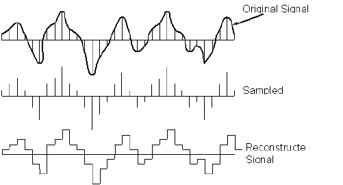
As you can see, ADC chips are an integral part of analog-digital devices. In the modern world it is very difficult to find a device that would not have ADCs. A classic view of the ADC is shown in the following figure.
')
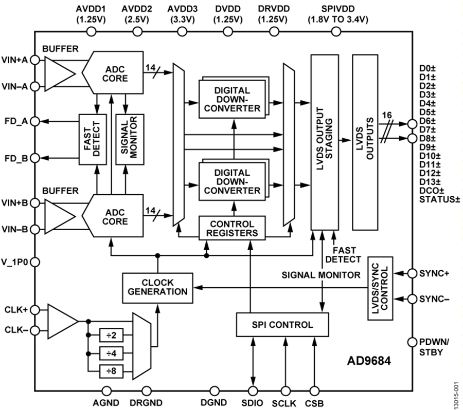
This is a simplified circuit taken from the datasheet on the AD9684 chip. It contains two differential analog inputs VINA and VINB , clock frequency input CLK , control via SPI interface, output bus in parallel form D0-D13 , power supply voltage points of various microcircuit nodes, SYNC synchronization unit and other control signals.
Obviously, ADC chips are characterized by a set of specific parameters on which the final choice of the user depends and which determines the scope of the ADC. On the digital side , this is the data transfer rate (effective clock frequency), which can be in the range of several tens of kHz to several GHz. The data width at the ADC output is in modern devices from 8 to 32 data bits. On the side of analog characteristics , this is the signal-to-noise ratio ( SNR ) and the dynamic range free of spurious components ( SFDR ), expressed, as a rule, in decibels (typical SNR levels are between 70-80 dB, and SFDR levels are around 90 dBc). Important parameters when choosing an ADC are - power dissipation (W), the number of channels in one package, the exchange interface with the digital node and, of course, the cost of the component.
Consider modern high-speed ADCs and their characteristics on the example of a table taken from the well-known Analog Devices website - a giant in the field of manufacturing all kinds of ADC and DAC chips. For convenience, the table summarizes the most important characteristics of the chips, they are divided according to the type of exchange interface with a digital device, and are arranged according to the speed of information transfer (clock frequency) from a higher value to a lower value.
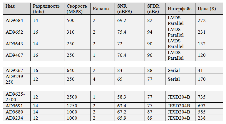
The table contains 4 high-end chips that transmit data in parallel form according to the LVDS standard. The data width of 14-16, channels 1-2, the maximum sampling rate of 500 MHz. The average SNR and SFDR values are 70 dBFS and 90 dBc, respectively. For some chips with a serial data transmission bus (Serial), the characteristics are almost the same. For modern ADC chips that use the JESD204B transmission interface and connect to the FPGA via gigabit lines, the clock frequencies are much higher, but the analog characteristics are slightly worse (at least due to the fact that the digital data is lower than 12 and 14 bits). In this article will not be considered connecting the ADC to FPGA crystals via gigabit lines. I will focus on a simple and well-studied version of the connection of microcircuits - a serial and parallel bus with data transfer interfaces such as LVTTL, LVDS, LVCMOS, LVPECL . In particular, an interesting method of data transmission over the LVDS bus, which is distinguished by the ease of tracing printed circuit boards, low cost performance, low noise and power dissipation, as well as high data transfer speeds. To receive data via a serial bus, FPGA uses serializers / deserializers. For a parallel bus, everything is much simpler and data is accepted as is.
In the course of work on the pairing of analog and digital devices, I had to learn the following ADC microcircuits. These are already outdated, but still used - AD9224, AD6644ST-65, AD9244, LCT2207, ADS5474, AD9432BST-105, AD7475BR , state-of-the- art ICs - AD9430BSV, ADS54RF, AD9467, ADC12D1800, AD9680 and others. Since the area of my work is only partially related to analog circuitry, I can hardly tell you about ways to improve the characteristics of complete analog-digital modules. Also, I will not be able to give advice on the qualitative construction of analog paths and the method of selecting those or other circuit components to achieve the best analog indicators (SNR, SFDR). But I will try to answer the questions of connecting the ADC to FPGA crystals and further data processing in this article.
Examples of ADC Modules
The following figures will present modern examples of complete and high-quality analog-to-digital data conversion modules from Russian and foreign manufacturers. All of them have one or several analog connection inputs and an FMC adapter connector (FPGA Mezzanine Card) for connection to the carrier board on which the data handler is installed (as a rule, this is FPGA). FMC is one of the main standards for connecting products on a modular architecture. An analog part is often installed on the mezzanine board (mezzanine board), and a central device is installed on the carier board, which performs data processing - it is one or more FPGAs and / or signal processors. Of the foreign manufacturers of devices should be allocated two leading manufacturing companies - this is 4dsp and hitechglobal. From domestic manufacturers, Google in the first lines of the search is issued by CJSC Scan Engineering Telecom, CJSC Tool Systems and others. The author of the article is not responsible for the presented modules and does not use the article in order to advertise the product of a company.
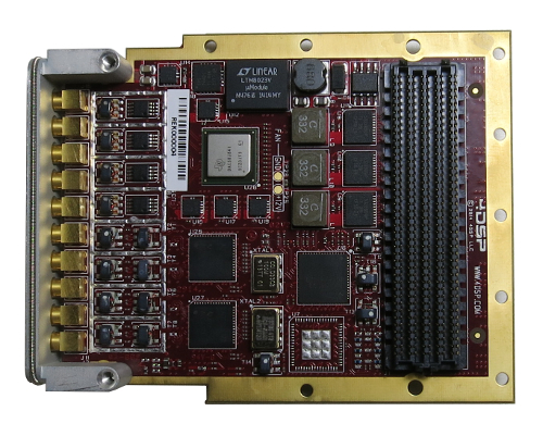
HTG-ADC16 . It has the following characteristics (taken from the official site):

- 16-Bit Resolution, Dual-Chanel, 1-GSPS ADC
- Noise Floor: –159 dBFS / Hz
- Spectral Performance (fIN = 170 MHz at –1 dBFS):
- SNR: 70 dBFS
- SFDR: 86 dBc
- SFDR: 96 dBc (Except HD2, HD3, and Interleaving Tones)
- Spectral Performance (fIN = 350 MHz at –1 dBFS):
- SNR: 67.5 dBFS
- NSD: –154.5 dBFS / Hz
- SFDR: 75 dBc
- SFDR: 85 dBc (Except HD2, HD3, and Interleaving Tones)
- Channel Isolation: 100 dBc at fIN = 170 MHz
- Input Full-Scale: 1.9 VPP
- Input Bandwidth (3 dB): 700 MHz
- On-chip dither
- Integrated Wideband DDC Block
- JESD204B Interface with Subclass 1 Support:
- 2 Lanes per ADC at 10.0 Gbps
- 4 Lanes per ADC at 5.0 Gbps
- Support for Multi-Chip Synchronization
- Power Dissipation: 1.35 W / ch at 1 GSPS
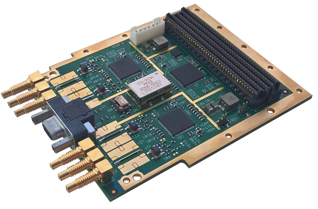
FMC104: 4-Channel 250 MSPS @ 14-bit . Characteristics (some removed due to redundancy of information):
- Four Channel 14-bit 250 MSPS A / D conversion
- Available as air cooled and conduction cooled
- VITA 57.1-2010 compliant
- Based on TI ADS62P49
- LVDS or 1.8V LVCMOS output operation
- Single ended AC- or DC-coupled analog input
- Flexible clock tree enables
- LPC (low-pin count) compatible
The feature of the module is four ADC channels, 1.8V supply voltage (HP-banks FPGA Xilinx are used).
FMC120: 4-Channel 250 MSPS @ 14-bit . Specifications:

- Quad - A / D - D / A Channel Operation
- Quad Channels 16-bit 1.00 GSPS A / D
- Quad Channels 16-bit 1.25 GSPS D / A
- Simultaneous sampling on all channels up to 1 GSPS
- VITA 57.1-2010 compliant
- Conduction Cooled - Standard Option
- Single ended DC or AC-coupled analog input.
- Clock Source, Sampling Frequency, and Calibration through SPI communication bus
- HPC - High Pin Count Connector
- 2Kbit EEPROM (24LC02B) accessible from the Host via I2C bus
- JTAG - CPLD device accessible from the FMC connection
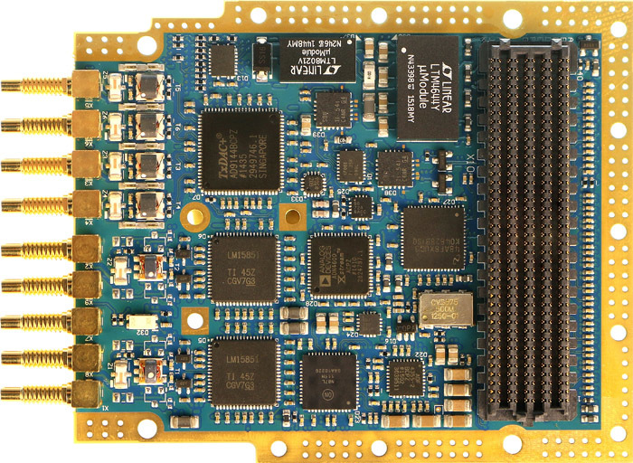
FMC140: 4-channel 16-bit 370MSPS A / D. It has the following characteristics:
- Four-channel, 16-bit A / D up to 370 MSPS
- VITA 57.1-2010 compliant
- JESD204B serial interface
- AC or DC-coupled analog signals
- SPI communication busses
- Flexible clock tree enables
- Power-down modes for switch power off
- HPC - High Pin Count connector
The feature of the module is 4 high-speed ADC channels, 16-bit data width, exchange via JESB204B interface.
Module SFM-4A1000 . Specifications:
- Four channels ADC: 14 bit 1000 MHz
- Broadband Transformer Input with bandwidth up to 2 GHz
- Interface with carrier module JESD204B
- Support for digital decimation and AGC functions built into the ADC
- Highly stable reference generator, external reference clock input
- Software control of ADC settings and clocking scheme
- Single-width FMC form factor with air or conductive cooling
The peculiarity of the module is domestic development, 4 high-speed ADC channels, 2 GHz band, exchange via JESB204B interface.
FMC212x4GDA module . Specifications:
- Two channels ADC 12 bit
- Conversion Frequency: 1 to 4 GSPS
- Analog input bandwidth: 5 to 2000 MHz
- Input resistance: 50 ohm
- DDC embedded in ADC
- Maximum DDC bandwidth: 800 MHz
- DDC decimation factor: 4 to 32
- Four channels D / A 16 bit 2.8 GSPS
- Interpolation: x2, x4, x8
- The frequency range of the output signals of the DAC: from 0.5 to 400 MHz
- Maximum output amplitude: ± 0.5 V
- Output impedance: 50 ohm
- ADC and DAC clock synthesizer with low phase noise
- ANSI / VITA 57.1 FMC module 69x76.5 mm
The feature of the module is 2 high-speed ADC channels, signal bandwidth up to 2 GHz, exchange via JESB204B interface, built-in DDC chips, 4 DAC channels.
FMC816x250M module . Specifications:
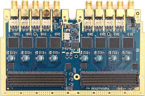
- ANSI / VITA 57.1 FMC double width module 139x76.5mm
- 8 ADC 16 bit
- Conversion frequency: 50 MHz to 250 MHz
- Analog input band 0.1 ... 250 MHz
- Conversion scales: ± 0.8V; ± 0.65V
- Input resistance: 50 ohm
- Internal / external clocking
- Tunable clock generator 10 ... 250 MHz
Module feature - 8 ADC channels, dual module.
As you can see, many of the analog-to-digital conversion modules in the FMC standard are similar and have almost identical characteristics, which are determined by the installed ADC and DAC chips. The final choice of a module is determined by the task that the end user needs to decide.
Connecting ADC to FPGA
Let us turn to the main section of the article - the connection of ADC chips to FPGA crystals. Consider connecting the ADC over parallel and serial bus, with data interfaces - LVTTL, LVCMOS, LVDS . The article will not consider connecting the ADC interface JESD204B , because it is the material of a separate topic, which will take more than one full article. In addition, JESD204B differs significantly in the implementation of the "classic" options for connecting ADC chips and requires more detailed consideration.
As is known, banks (pin groups) of I / O FPGAs can be configured for different supply voltages, the boundaries of which are determined by the manufacturer of the crystals. In modern FPGAs of the Xilinx type, the voltage range applied depends on the type of bank. There are two main types of banks (Xilinx) - HP (high-performance) and HR (banks with a large selection of standards and power). For example, in chips 7 of the Xilinx series, the voltage range for HR banks is from 1.2 to 3.3V, and for HP banks - from 1.2 to 1.8V. In addition, banks' pins can be programmed for a wide range of standard data transfer interfaces, but the final choice of a standard is determined by two rules: the supply voltage of the FPGA bank and the method of connecting the remote device and the FPGA. On the other hand, an important factor in the choice of the voltage supply of the FPGA bank is a family of crystals. So, for Kintex-7 it is possible to use the LVDS 25 standard and supply a 2.5V bank, and for many FPGA Virtex-7 chips, the connection standard is exclusively LVDS 18, and the bank is powered by 1.8V. In this regard, the problem arises of pairing some analog modules and carrier boards with different FPGA families. Therefore, when you purchase an ADC module and / or carrier card from a third-party manufacturer, you need to make sure that they are compatible with the standard and the supply voltage. As a rule, the data transfer interface is written in the constraint file ( UCF or XDC ), and not in the project source codes, which provides configuration flexibility and reuse of source files in other projects.
The block diagram of the project's top-level file (as well as the internal blocks used to receive data from ADC chips according to the LVTTL / LVCMOS / LVDS standard) is presented in the following figure.
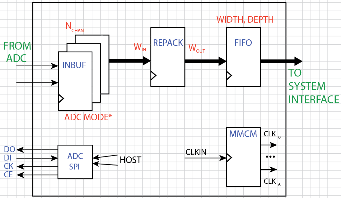
It includes the following elements:
- Input receiver
- Data packer
- Data Flow Synchronizer (FIFO)
- The control unit chips ADC
In addition to these nodes, at the top level, the MMCM-based frequency synthesis module is used - a standard FPGA resource. The IDELAYCTRL component is also used to control delays in the IODELAY nodes.
The main parameters of the top-level file on which the FPGA scheme configuration depends:
- NCHAN - the number of independent ADC channels,
- DATA_WIDTH - the data width of the ADC,
- FIFO_ADDR - FIFO depth: DEPTH = 2 ** ADDR,
- DATA_RATE - data reception mode: SDR / DDR,
- PACK_OUT - width of the output bus of the packer (system bus),
- CLK_SEL - select the main clock source for the multichannel circuit,
- USE_MMCM - using the MMCM node instead of BUFR to divide the CLKDIV frequency by SERDES,
- DIFF_TERM - using differential input signals (TRUE / FALSE),
- IOSTANDARD - voltage standard for LVDS lines,
- DATA_IOBDELAY_TYPE - the operation mode of the IODELAY delay node,
- DATA_IOBDELAY_VALUE - default delay value,
- DIFF_CLOCK - use differential input clock (TRUE / FALSE),
- OVR_PRES - using the ADC overflow lines (overflow),
- STR_PRES - use the ADC external start signal lines (start),
- RESYNC_OUT - enable the mechanism of primary resynchronization of data on the input buffer (YES / NO).
And some other options.
The part of the code file of the top-level ADC receiver looks like this:
xFIFO: CTRL_FIFO_CONFIG generic map ( DATA_WIDTH => PACK_OUT, ADDR_WIDTH => FIFO_ADDR ) port map ( reset => reset, wr_clk => clk_pack, rd_clk => sys_clk, data_i => do_pack, data_o => do_fifo, rd_en => cs_fifo, wr_en => dv_pack, empty => ef_fifo, full => ff_fifo ); This is where the FIFO node connects to synchronize data with the device's system bus. Programming delays for IODELAY in a multichannel and multi-bit buffer scheme is as follows:
---- Data delays ---- x_dat_dd <= x_dat_do(conv_integer(unsigned(dl_chan))) when rising_edge(dl_clk); x_dat_in(conv_integer(unsigned(dl_chan)))(conv_integer(unsigned(dl_muxs))) <= dl_dat_in when rising_edge(dl_clk); x_dat_ce(conv_integer(unsigned(dl_chan)))(conv_integer(unsigned(dl_muxs))) <= dl_dat_ce when rising_edge(dl_clk); x_dat_ld(conv_integer(unsigned(dl_chan)))(conv_integer(unsigned(dl_muxs))) <= dl_dat_ld when rising_edge(dl_clk); Where dl_chan is the selected ADC channel, dl_muxs is the selected ADC bit. This is done for independent programming of every bit of data.
Consider each node in detail.
Note: for connecting FPGAs and D / A converters (D / A converters), the situation is mirrored. It is necessary to do everything the same, but in reverse order. In this article, the connection of the FPGA to the DAC is not considered.
Input receiver
It contains the primary elements of the connection between the external signals of the circuit board and the logic of the FPGA. This is the IPAD buffer from the FPGA pin to the IOBUF input buffer logic . Depending on the data transfer interface, the buffer may be differential - IBUFDS and unipolar - IBUF. For many buffers, a hard link to the required standard is possible, or it is possible to set the type of output signal through attributes. For example, for IBUFDS, using the IOSTANDARD attribute, you can define and set the standard " LVDS_25 " in advance in the source codes.
Behind the buffer, a node for controlling the delay of the IODELAY signal passing is set to align the edges of the parallel data bus and to first match the multi-channel nodes connecting the ADC to the FPGA. IODELAY is a programmable FPGA resource, the delay value can be fixed and determined by the default setting, or programmed in the range from 0 to 31 conventional time values (the digit is determined by the FPGA datasheet). Programming is done in a primitive way with the help of several signals. We will not dwell on the detailed analysis of the programming algorithm; for more information, you can refer to the document from the list of references at the end of the article. For IODELAY nodes, you need to connect a special IDELAYCTRL delay control node , which real-time calibrates the delays for each FPGA clock region. To eliminate the influence of the crystal temperature, the supply voltage and the load on the FPGA, the IDELAYCTRL node is clocked with an independent REFCLK signal. This clock signal provides an equal amount of delay ( TAP ) in all IODELAY nodes of each FPGA clock region. If each clock region needs its own trim values, several IDELAYCTRL nodes are initialized in the FPGA chip. The clock signal REFCLK can be supplied from an external generator installed outside the FPGA, or it can be obtained by synthesizing a frequency at the FPGA crystal MMCM node.

Following the IODELAY delay node, the FD trigger can be set if the data transfer mode is DATA_RATE = “ SDR ”. This trigger is optionally placed in the input buffer and clocked by the ADC frequency that accompanies the data from the analog module. In the DATA_RATE = " DDR " mode, the trigger is replaced with a sophisticated version of IDDR , which has one data input and two outputs. From the output, data can be output in several modes, but in practice I used only one - this is “ SAME_EDGE_PIPELINED ”, in which data from the output of Q1 and Q2 are output on the same edge of the clock signal.
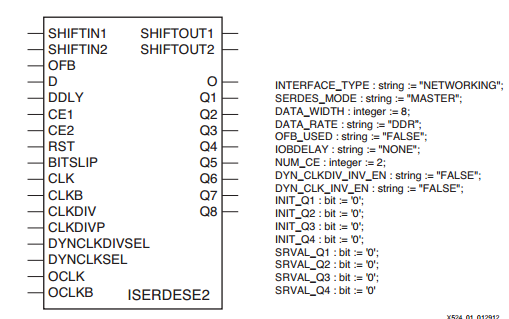
Finally, the most interesting option is to connect the IODELAY node to the ISERDES data deserialization module . The serializer node is a complex element of the FPGA input buffer, it contains the following options:
- DATA_RATE - defines the output mode ( SDR / DDR),
- DATA_WIDTH - determines the width of the data bus at the node output (from 1 to 8),
- INTERFACE_TYPE - type of data interface. To connect the ADC chips, the “ NETWORKING ” mode is used.
- SERDES_MODE - connection mode ISERDES in the case of using multiple serializers to receive data from one FPGA contact.
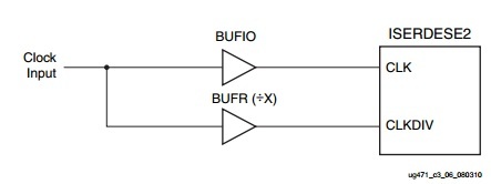
A node clock is triggered by several signals — this is the signal at the high frequency of the received CLK data and the signal CLKDIV divided by the number defined by the DATA_WIDTH parameter. Fission can occur outside the FPGA, but in practice, frequency synthesizers are used in the FPGA chip itself, which are called MMCM. Thus, a serial signal at the CLK frequency is input to the ISERDES node, and a parallel data stream is obtained at the ISERDES node output at the reduced frequency CLKDIV = CLK / DATA_WIDTH . The clock frequency can be divided using the regional buffer BUFR , the value of the division factor BUFR_DIVIDE = 1-8, or on the MMCM frequency synthesizer node, programmed in a wide range.
To eliminate the effect of coincidence of the clock and data edge, IODELAY nodes and frequency adjustment in the MMCM are not always enough. Often it is necessary to look for alternative ways to solve this problem. Fortunately, this solution was found by my colleague, which he recently talked about in his article ( Useful Properties of Jitter ).
All of the above nodes (with the exception of MMCM) are part of the input FPGA buffer and do not occupy the logical resources of the crystal. From the FD / IDDR / ISERDES output, the data already arrive at the logic elements — this is a small trigger or FIFO for primary resynchronization of data to the frequency obtained after passing the ADC sampling frequency at the MMCM node. In some cases, resynchronization is not used, and the data is synchronized directly by the ADC sampling rate. The following figure shows a timing diagram for processing serial data from an ADC chip on an ISERDES device. The input clock frequency, the serial input data, and the converted data into parallel code are shown.
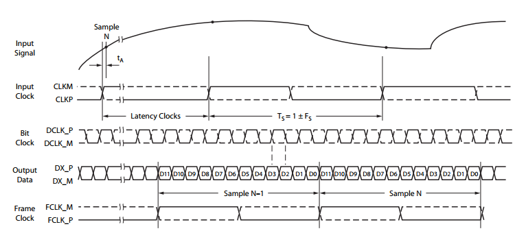
Thus, depending on the configuration, there are three possible signal paths in the input buffer, as shown in the figure:
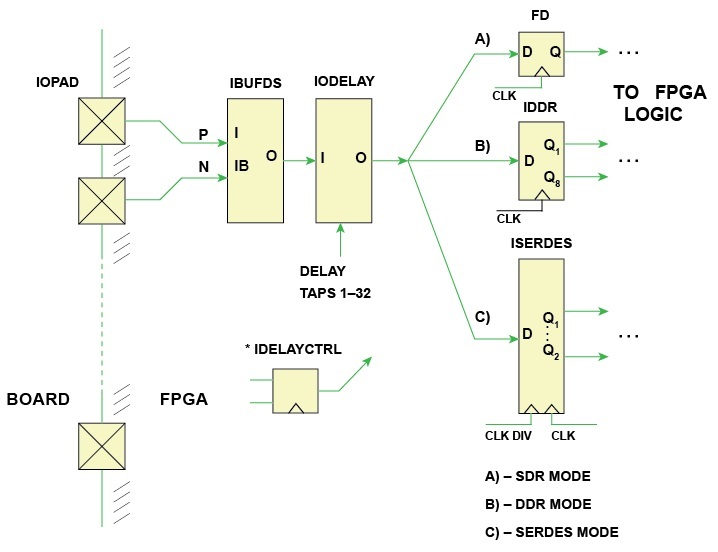
A) SDR mode - data is received via a parallel bus, for each data bit its FPGA buffer is used,
B) DDR mode - data is received on a parallel bus, data is clocked by double the frequency.
C) SERDES mode - data is received via serial bus
Data packer
This node is used in single-channel and multichannel data reception circuits from the ADC. Its main purpose is to pack the data into a convenient internal bus format used inside the FPGA. The internal bus width is determined by the developer or corporate standard. Typical values of bitness at the packer output are 32, 64, 128, 256, 512 data bits. In some cases, the packer cannot be configured. It depends on the number of input channels, the width of the input and output data bus packer. For example, for a four-channel source with input data width = 16 bits, it is impossible to organize a repacker with an output bus that is less than WOUT = WIN * NCHAN = 16 * 4 = 64 bits. For a single-channel data source with the same bit width at the input and output, the data will be sequentially packed in packs of 16 bits into a 64-bit bit grid. That is, the first ADC countdown will take the bit field [15: 0], the second countdown - [31:16], the third one - [47:32], and the fourth one - [63:48]. Further, the samples will cyclically occupy bit fields from the lowest to the highest in the output data grid. Another example. 2 data channels are used, the bit widths at the input and output remain the same - 16 and 64 bits, respectively. If the data acquisition system on the remote device includes only one channel, then the packaging occurs, as shown in the example above, and it does not matter which channel is included. If the acquisition system includes both channels, then the data is packed in pairs from the lower part of the discharge grid to the older one. The first reading of the first channel will take the position [15: 0], the first reading of the second channel will take the position [31:16], the second reading of the first channel - [47:32], the second reading of the second channel - [63:48]. As practice has shown, this is the most convenient way to pack data for multichannel processing, in the case of disconnection of certain transmission channels. Note: the number of channels must be a multiple of the power of two - 1, 2, 4, 8, etc. It may seem that this site is difficult to implement and understand, but after several applications in your projects you will find for yourself that there is nothing complicated or unusual here.
The following figure shows time diagrams of the data packer node operation in the mode: NCHAN = 1, WIN = 8, WOUT = 32.
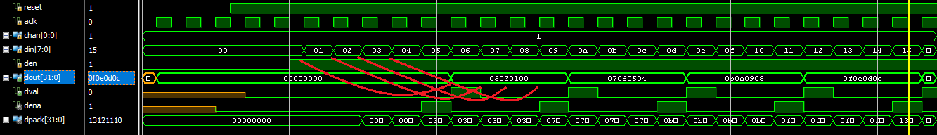
The red lines show the process of data packing to the output bus, which is accompanied by a DVAL = 1 resolution signal after receiving 4 data samples.
Data stream synchronizer
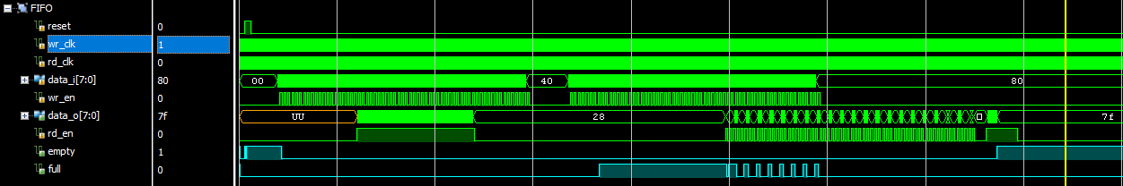
This node is built on the basis of a primitive FIFO scheme and has one important and simple purpose — converting the data stream from the sampling frequency CLK_ADC to the processing frequency or the frequency of the internal bus of the SYS_CLK device (system clock frequency). For simplicity, you can create a FIFO node in the Xilinx Core Generator , but ideally it is better to write your own module, which will be flexible in configuration to an arbitrary bus width ( FIFO_WIDTH ) and memory depth ( FIFO_DEPTH ). The following figure shows time diagrams of the FIFO node operation, shows the input and output data, as well as the empty and full FIFO flags. It should be noted that for the FIFO ADC to work properly, the FULL full flag must always be 0, which indicates the correctness of data received from the ADC and the absence of overflow. If the FULL flag = 1, then the data reception rate of the remote processor is insufficient, or the ADC operation speed is too high for the selected system.
The following figure shows a schematic representation of the FIFO node in the Plan Ahead environment.
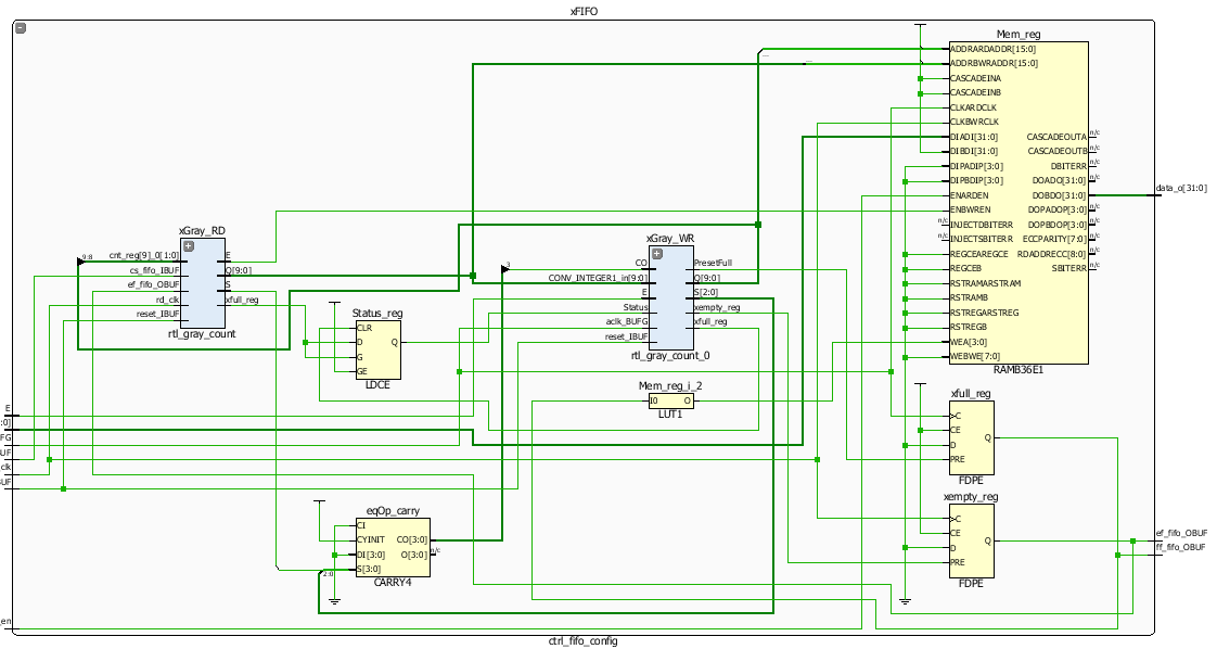
It can be seen that the FIFO is built on the basis of dual-port memory. On the memory bus address data is sent in gray code - in the diagram there are two nodes for reading and writing. This allows to reduce the bit error at high frequencies, since neighboring values in the gray code differ only in one bit position. The logic of the FIFO flags is determined by the values in the Gray Counter modules, and the registers are used to increase the clock frequency of the node.
Inner tire
The question arises - where does the collected and packed data go further ? The answer is simple: with the help of interfaces PCI / PCIe, USB, Ethernet, SRIO, SATA, the data reach the final goal, where they undergo further processing and where all information is collected. Prior to this link, a digital signal processing (DSP) node can be inside the FPGA, for example, DDC, DUC, FFT / IFFT , etc. In addition, data can be buffered on external high-capacity memory, such as DDR3 / DDR4 .This is a frequent technique that is used to process a large flow of information at high speeds. In this case, the external memory simulates a large FIFO. To connect the FPGA with external memory, special controllers are used, which, as a rule, are accessible and open for use. In the case of Xilinx, they are in the IP Core Generator.
Among other things, the developer needs to create his own control state machine.all ADC receiver resources: this is the configuration of delays in IODELAY, programming of the MMCM frequency synthesizer, sending commands via SPI to ADC and DAC modules, controlling the beginning and end of data collection from the ADC, managing the number of active channels, using external DDR memory and much more. All have their own unique architecture, but the basic principles remain the same. In the company in which I work, control nodes called " tetrads " are used. My colleague told about them in detail here .
Control of the ADC module
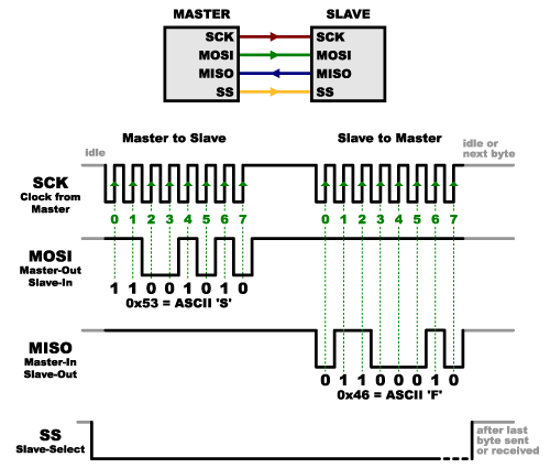
As a rule, the analog module is controlled via SPI-like interfaces. Implement the SPI-interface under the power of any senior student, in the program of which there is a study of programmable logic and FPGA. Focus on the SPI node, I will not. At the end of the article, as an example, the source control code of the remote HI-6131 chip is given , which processes messages in the MIL-STD-1553 format . The code is not parameterizable and sharpened specifically on the selected chip. To warm up, you can write your SPI node, which will be configured for different parameters. The timing diagram of control over the SPI interface is as follows:
Source
The source code of all components and assemblies is presented in the VHDL language and is intended for FPGA Xilinx 7 series chips (and above). Source codes are open for use and are available via the link on the githaba - see here . All components are made as flexible as possible in the configuration and do not require significant intervention in the source code (with the exception of the SPI node -
For example, the read and write operations in the FIFO, as well as the connection of the binary-to-gray conversion nodes look like this:
FIFO R / W
---- Read data ---- pr_rd: process(rd_clk) begin if (rising_edge(rd_clk)) then if (rd_en = '1' and xempty = '0') then data_o <= Mem(conv_integer(pNextWordToRead)); end if; end if; end process; ---- Write data ---- pr_wr: process (wr_clk) begin if (rising_edge(wr_clk)) then if (wr_en = '1' and xfull = '0') then Mem(conv_integer(pNextWordToWrite)) <= data_i; end if; end if; end process; ---- Gray counters ---- xGray_WR : rtl_gray_count generic map ( COUNTER_WIDTH => ADDR_WIDTH ) port map ( cnt => pNextWordToWrite, ena => NextWriteAddressEn, rst => reset, clk => wr_clk ); xGray_RD : rtl_gray_count generic map ( COUNTER_WIDTH => ADDR_WIDTH ) port map ( cnt => pNextWordToRead, ena => NextReadAddressEn, rst => reset, clk => rd_clk ); Bibliography
- 7 Series FPGAs Overview (DS180) (xilinx.com)
- Xilinx 7 Series Libraries Guide for Schematic Designs (xilinx.com)
- 7 Series FPGAs SelectIO Resources User Guide (UG471) (xilinx.com)
- 7 Series FPGAs Clocking Resources User Guide (UG472) (xilinx.com)
- Serial LVDS High-Speed ADC Interface (xilinx.com)
- Analog for Xilinx ® FPGAs Selection Guide (ti.com)
- HSC-ADC-FPGA High Speed Deserialization (analog.com)
- Interfacing Analog to Digital Converters to FPGAs (latticesemi.com)
To be continued...
Source: https://habr.com/ru/post/313692/
All Articles