All you wanted to know about the design and manufacture of chips, but hesitate to ask
Lord I already wrote about the upcoming seminars of Charles Danchek, containing a complete educational program on all stages of the design and production of microcircuits , but since then there have been additions:
* First, Cadence Design Systems, one of the two leading companies in the field of circuit design automation, joined the workshops. Cadence will present an hourly report with the program at the end of this post.
Registration on the site (UPD: apparently, the initial registration is overfilled. But the Rosan officials said that if the first hall is full, they will allocate a larger room. Write an email to the post office ).
')
* Secondly, four leading Russian chip design companies joined the seminars: NIIMA Progress JSC, BAIKAL ELECTRONICS JSC, LABSISTEMS LLC and ELTC JSC. Each of them will make a public presentation with information that you, under other circumstances, usually cannot get without NDA.
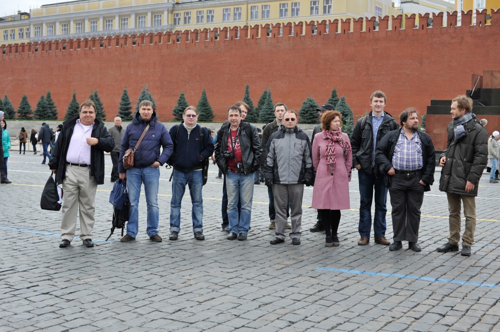
* Third, in addition to the official program of seminars in Moscow, St. Petersburg and Kiev, we decided to organize informal meetings for those interested in a walk first in Moscow on this Sunday, October 30th. You can show Charles Danchek Moscow (he is the first time in Russia) and ask about chip design.
We are thinking of expanding such activities in the Novosibirsk-Tomsk region in the following year, in connection with which, here is a welcome video with a girl from the Novosibirsk Academgorodok:
Explanation: RUSNANO and MISiS organize a Nanometer ASIC seminar in Moscow, but in St. Petersburg such a seminar is organized by ITMO University, and in Kiev - KPI and KNU, Lamp's laboratory of KPI and student workspace “Belka” KPI.
Details about the meeting and seminars - under the cut:
The format of the informal meeting will be the same as the format of last year’s meeting (which really was without Charles Danchek). We meet at 12 noon on Sunday, October 30, the Smolenskaya metro exit of the blue metro line (we adopted the tradition of the meeting point from MEPI-Schnick). After that, we go to dinner at 3 pm in Jean-Jacques on Nikitsky Boulevard to reposition Jean-Jacques from the meeting place of creative humanities to the meeting place of the harsh engineers of the microelectronic industry.
If you are late, call me (Yuri Panchul) at +7 925 022 5427
Information about the seminar "Specialized Nano-Level Integrated Circuits"
The workshop introduces students to the phased development of special-purpose integrated circuits (hereinafter - ASIC) using nanoscale technologies (32 nm and below).
Information about the lecturer: Charles Danchek (Charles Dancak)
International expert, professor at the University of California at Santa Cruz in Silicon Valley, engineer of the executive office of Synopsys for 10 years.
Received MSEE at the University of Wisconsin (Madison), as well as a master's degree in solid state physics at the Polytechnic Institute in New York (Brooklyn). He taught in eight countries. He worked for Teradyne, Cadence and Silicon Compilers.
The following issues will be addressed during the seminar:
• The principles of operation of the elements AND NOT and OR NOT, the topology of a standard cell suitable for synthesis.
• Specification of CMOS chip as a product on paper: characteristics table; feasibility study; chip cost
• ASIC business ecosystem without own production facilities (fabless); process options; plates for shuttle launches; other key planning details.
• Illustrative example: Broadcom 1103 CMOS Ethernet IP phone chip (CMOS chip for IP telephony).
• Example: writing RTL code for a simple digital function on SystemVerilog.
• How VLSI synthesis tools convert an RTL description into optimized circuits from standard cells.
• Calculation of delays at the logical level, based on data from standard library cells and estimated values of the chain lengths.
• Synthesis of RTL code into logic specific to a particular technology. Imposing restrictions on the period of the clock signals.
• Timing characteristics of one clock cycle: can new data pass a critical path in one cycle.
• Writing RTL statements by analogy with executable comments, which are verified by means of simulators or FEC (formal verification) tools.
Subsection: IP Block Design
• IP block formats: software (synthesized), hardware (reprogrammable), topologically hard. How format affects the price.
• Types of IP-blocks: central processing unit (CPU), digital signal processing processor (DSP), graphics processing unit (GPU), radio signal processing unit (RPU), cryptography, digital interfaces, analog circuits.
• Classes of IP blocks of the central processor: blocks of the initial level for the MCU and IoT, the middle level for efficient embedded systems, high-performance level. Multi-core blocks; homogeneous and heterogeneous calculations.
• Tires and nets on chip. Using the interface constructs of the SystemVerilog language to encapsulate bus connections with concise and reusable coding.
Subsection: radio frequency / analog design
• A typical design route for on-chip RF / wireless design that is immune to process variations.
• Example: designing a voltage controlled generator (VCO), up to the GDSII topology.
• Writing a Verilog-AMS model VCO to detect errors like incorrect polarity or crossed signals.
• Evolution of the test bench: from a simple unit-level bench to a multi-level system bench using transactions; limited incidental exposure (CRV); built-in SystemVerilog statements; criterion of coverage.
• Formal equivalence test for confirmation: the functionality will not change after the introduction of scan chains, the introduction of a clock signal and changes made in manual mode (ECOs).
• Hardware emulation: build a hardware model based on FPGA, which is ideal for early debugging for a chip that is under development but not yet manufactured.
• Synthesis of verified source RTL code, meeting time requirements, area restrictions, etc.
• Processing of clock signals during logical synthesis and physical design. Convergence of the sync domain.
• Violation of temporal characteristics. Methods of correction. Calculate the delays of elements and chains.
• Physical design stages: topological planning, placement of standard cells, clock signal tree synthesis, tracing.
• Preparing the crystal for production: electrical power distribution, elimination of overloads or excessive voltage drop (IR drop), design rules checking (DRC).
Subsection: Design for Testing
• Inserting the system scan chain, generating test patterns for detecting errors such as constant, bridging and delay errors.
• Built-in self-diagnosis for memory blocks (MBIST) and logical blocks (LBIST and STUMPS).
• Organization of peripheral scanning on the periphery of the chip for testing at the board level.
Subdivision: transfer to production
• What are the causes of violation of the integrity of signals like cross-talk?
• What are geometric (DRC) and electrical (ERC) rules. Why use non-standard rules.
• Verification of the topology and schema (LVS) in order to confirm the compliance of the topology with the schematic description.
• General GDSII file, a geometric description of the traced topology of the entire crystal.
• Download GDSII file for the production of masks. Preparing to create a mask (OPC).
• How the GDSII database is used to create a set of precise masks or photo masks. What limits resolution?
• Main manufacturing methods: photolithography, oxidation, ion implantation, metallization, IMD, CMP.
• How innovative developments like dual lithography ensure Moore’s law in the present and the future.
Subsection: FEOL production (application of semiconductor structures)
• Shallow-trench isolation - the secret for economical processing of CMOS plates.
• Shaping polysilicon (including HKMG) and drain / source implantation.
• Production of complementary transistors of n and p type - the basis of the inverter.
Subsection: BEOL production (deposition of metal layers)
• How to apply a layer of Metal 1 by applying a copper ornament (copper damascene processing).
• Isolation of each metal layer from the next (IMD), the formation of contacts / transitional interlayer compounds.
• Flipping plates designed for flip-chip packaging. Wire-bond.
• Plate breaking: testing to identify suitable packaging crystals.
Crystal packing using flip-chip or wire-bond, testing, checking for minimum speed and rejection for use in the customer's system during the product's useful life. Includes:
Subsection: Chassis Design and Assembly
• Joint development of housing: electrical, thermal, mechanical considerations.
• Flip-chip and wire-bonding technologies.
• Signal flow outside the crystal, through metal layers, RDL layer, bumps, output for PC board. Modeling the effect of the body.
• Silicon transitions and 3D packaging technology.
Subsection: Testing and Diagnostics
• Within ATE: How the test vector detects one constant error out of millions on the chip.
• Shmoo plots (text-graphic diagrams); analysis of the chip operation under technologically boundary conditions.
• Functional testing on the frequency range; measurement of fmax and static Iddq.
Subsection: Silicon Check
• Development of a test board with user (FPGA) equipment for testing the device at the required frequency.
• Using logic analyzers, scan-logs, JTAG ports and, often, on-chip instrumentation.
• Error correction techniques associated with metal mask corrections of layers that allow the use of spare elements or triggers.
The seminar will present examples of how CAD tools are used in real projects of JSC NIIMA Progress, JSC BAIKAL ELECTRONICS, LLC LABSISTEMS and JSC R & D Center ELVIS.
Two examples of Cadence software from other seminars and exhibitions:
1. The tool for Genus synthesis is a fragment of its presentation in June at the Design Automation Conference 2015 in San Francisco:

2. Simulation and verification. Here is how the debugging of the MIPS microAptiv UP processor core from the MIPSfpga package in SimVision looks like. The names of the mpc_ waveform signals on the waveform are the master pipeline control :

* First, Cadence Design Systems, one of the two leading companies in the field of circuit design automation, joined the workshops. Cadence will present an hourly report with the program at the end of this post.
Registration on the site (UPD: apparently, the initial registration is overfilled. But the Rosan officials said that if the first hall is full, they will allocate a larger room. Write an email to the post office ).
')
* Secondly, four leading Russian chip design companies joined the seminars: NIIMA Progress JSC, BAIKAL ELECTRONICS JSC, LABSISTEMS LLC and ELTC JSC. Each of them will make a public presentation with information that you, under other circumstances, usually cannot get without NDA.
* Third, in addition to the official program of seminars in Moscow, St. Petersburg and Kiev, we decided to organize informal meetings for those interested in a walk first in Moscow on this Sunday, October 30th. You can show Charles Danchek Moscow (he is the first time in Russia) and ask about chip design.
We are thinking of expanding such activities in the Novosibirsk-Tomsk region in the following year, in connection with which, here is a welcome video with a girl from the Novosibirsk Academgorodok:
Explanation: RUSNANO and MISiS organize a Nanometer ASIC seminar in Moscow, but in St. Petersburg such a seminar is organized by ITMO University, and in Kiev - KPI and KNU, Lamp's laboratory of KPI and student workspace “Belka” KPI.
Details about the meeting and seminars - under the cut:
The format of the informal meeting will be the same as the format of last year’s meeting (which really was without Charles Danchek). We meet at 12 noon on Sunday, October 30, the Smolenskaya metro exit of the blue metro line (we adopted the tradition of the meeting point from MEPI-Schnick). After that, we go to dinner at 3 pm in Jean-Jacques on Nikitsky Boulevard to reposition Jean-Jacques from the meeting place of creative humanities to the meeting place of the harsh engineers of the microelectronic industry.
If you are late, call me (Yuri Panchul) at +7 925 022 5427
Information about the seminar "Specialized Nano-Level Integrated Circuits"
The workshop introduces students to the phased development of special-purpose integrated circuits (hereinafter - ASIC) using nanoscale technologies (32 nm and below).
Information about the lecturer: Charles Danchek (Charles Dancak)
International expert, professor at the University of California at Santa Cruz in Silicon Valley, engineer of the executive office of Synopsys for 10 years.
Received MSEE at the University of Wisconsin (Madison), as well as a master's degree in solid state physics at the Polytechnic Institute in New York (Brooklyn). He taught in eight countries. He worked for Teradyne, Cadence and Silicon Compilers.
The following issues will be addressed during the seminar:
STEP 1: SPECIFICATION
• The principles of operation of the elements AND NOT and OR NOT, the topology of a standard cell suitable for synthesis.
• Specification of CMOS chip as a product on paper: characteristics table; feasibility study; chip cost
• ASIC business ecosystem without own production facilities (fabless); process options; plates for shuttle launches; other key planning details.
• Illustrative example: Broadcom 1103 CMOS Ethernet IP phone chip (CMOS chip for IP telephony).
STAGE 2: PRACTICAL DEVELOPMENT
• Example: writing RTL code for a simple digital function on SystemVerilog.
• How VLSI synthesis tools convert an RTL description into optimized circuits from standard cells.
• Calculation of delays at the logical level, based on data from standard library cells and estimated values of the chain lengths.
• Synthesis of RTL code into logic specific to a particular technology. Imposing restrictions on the period of the clock signals.
• Timing characteristics of one clock cycle: can new data pass a critical path in one cycle.
• Writing RTL statements by analogy with executable comments, which are verified by means of simulators or FEC (formal verification) tools.
Subsection: IP Block Design
• IP block formats: software (synthesized), hardware (reprogrammable), topologically hard. How format affects the price.
• Types of IP-blocks: central processing unit (CPU), digital signal processing processor (DSP), graphics processing unit (GPU), radio signal processing unit (RPU), cryptography, digital interfaces, analog circuits.
• Classes of IP blocks of the central processor: blocks of the initial level for the MCU and IoT, the middle level for efficient embedded systems, high-performance level. Multi-core blocks; homogeneous and heterogeneous calculations.
• Tires and nets on chip. Using the interface constructs of the SystemVerilog language to encapsulate bus connections with concise and reusable coding.
Subsection: radio frequency / analog design
• A typical design route for on-chip RF / wireless design that is immune to process variations.
• Example: designing a voltage controlled generator (VCO), up to the GDSII topology.
• Writing a Verilog-AMS model VCO to detect errors like incorrect polarity or crossed signals.
STAGE 3: FUNCTIONAL VERIFICATION
• Evolution of the test bench: from a simple unit-level bench to a multi-level system bench using transactions; limited incidental exposure (CRV); built-in SystemVerilog statements; criterion of coverage.
• Formal equivalence test for confirmation: the functionality will not change after the introduction of scan chains, the introduction of a clock signal and changes made in manual mode (ECOs).
• Hardware emulation: build a hardware model based on FPGA, which is ideal for early debugging for a chip that is under development but not yet manufactured.
STAGE 4: IMPLEMENTATION
• Synthesis of verified source RTL code, meeting time requirements, area restrictions, etc.
• Processing of clock signals during logical synthesis and physical design. Convergence of the sync domain.
• Violation of temporal characteristics. Methods of correction. Calculate the delays of elements and chains.
• Physical design stages: topological planning, placement of standard cells, clock signal tree synthesis, tracing.
• Preparing the crystal for production: electrical power distribution, elimination of overloads or excessive voltage drop (IR drop), design rules checking (DRC).
Subsection: Design for Testing
• Inserting the system scan chain, generating test patterns for detecting errors such as constant, bridging and delay errors.
• Built-in self-diagnosis for memory blocks (MBIST) and logical blocks (LBIST and STUMPS).
• Organization of peripheral scanning on the periphery of the chip for testing at the board level.
Subdivision: transfer to production
• What are the causes of violation of the integrity of signals like cross-talk?
• What are geometric (DRC) and electrical (ERC) rules. Why use non-standard rules.
• Verification of the topology and schema (LVS) in order to confirm the compliance of the topology with the schematic description.
• General GDSII file, a geometric description of the traced topology of the entire crystal.
• Download GDSII file for the production of masks. Preparing to create a mask (OPC).
STAGE 5: PRODUCTION
• How the GDSII database is used to create a set of precise masks or photo masks. What limits resolution?
• Main manufacturing methods: photolithography, oxidation, ion implantation, metallization, IMD, CMP.
• How innovative developments like dual lithography ensure Moore’s law in the present and the future.
Subsection: FEOL production (application of semiconductor structures)
• Shallow-trench isolation - the secret for economical processing of CMOS plates.
• Shaping polysilicon (including HKMG) and drain / source implantation.
• Production of complementary transistors of n and p type - the basis of the inverter.
Subsection: BEOL production (deposition of metal layers)
• How to apply a layer of Metal 1 by applying a copper ornament (copper damascene processing).
• Isolation of each metal layer from the next (IMD), the formation of contacts / transitional interlayer compounds.
• Flipping plates designed for flip-chip packaging. Wire-bond.
• Plate breaking: testing to identify suitable packaging crystals.
STEP 6: DISPOSAL
Crystal packing using flip-chip or wire-bond, testing, checking for minimum speed and rejection for use in the customer's system during the product's useful life. Includes:
Subsection: Chassis Design and Assembly
• Joint development of housing: electrical, thermal, mechanical considerations.
• Flip-chip and wire-bonding technologies.
• Signal flow outside the crystal, through metal layers, RDL layer, bumps, output for PC board. Modeling the effect of the body.
• Silicon transitions and 3D packaging technology.
Subsection: Testing and Diagnostics
• Within ATE: How the test vector detects one constant error out of millions on the chip.
• Shmoo plots (text-graphic diagrams); analysis of the chip operation under technologically boundary conditions.
• Functional testing on the frequency range; measurement of fmax and static Iddq.
Subsection: Silicon Check
• Development of a test board with user (FPGA) equipment for testing the device at the required frequency.
• Using logic analyzers, scan-logs, JTAG ports and, often, on-chip instrumentation.
• Error correction techniques associated with metal mask corrections of layers that allow the use of spare elements or triggers.
The seminar will present examples of how CAD tools are used in real projects of JSC NIIMA Progress, JSC BAIKAL ELECTRONICS, LLC LABSISTEMS and JSC R & D Center ELVIS.
The program of the seminar “Specialized Integrated Circuits of the Nano-Level”
Venue: NITU "MISiS", main building, auditorium B-636.
10/31/16
9.00–9.30 Registration
9.30–9.45 Presentation of the speaker
9.45–10.45 Stage 1: Specification
Chips: basic concepts, historical view, key discoveries, switches of n-type and p-type, CMOS logic.
10.45—11.00 Break
11.00–12.00 Stage 1: Description of the IC (continued)
Ecosystem Fabless SBIS. The cost of the chip.
12.00-13.00 Stage 2: Practical development
Writing RTL code on SystemVerilog for a simple logical function (serializer, serializer). Netlist synthesis based on standard cells. Calculation of delays. One sync cycle. Correction of sync violations. RTL approval.
Demo-case of JSC "NIIMA Progress".
13.00–14.00 Lunch
14.00–15.00 Stage 2: Practical development (continued)
[joint presentation with Yuri Panchul, Imagination Technologies]
Subsection: Designing Systems on a Crystal (SoC) based on IP cores and buses. The main types of IP-cores. Tires and interfaces on a crystal.
Demo case of JSC BAIKAL ELECTRONICS.
15.00–15.15 Break
15: 15–16.00 Stage 2: Practical Development (continued)
Subsection: radio frequency (RF) / analog design and simulation.
16.00–17.30 Stage 3: Functional Verification
The evolution of test cases, from basic at the block level to multilayer at the system level. Verification of random samples with constraints (CRV). SystemVerilog approval control. Formal Equivalence Verification (FEC). FPGA-based hardware emulation.
17.30–18.00 Results:
Discussion, questions and answers.
18.00–19.00 Thematic presentation by Cadence Design Systems
"The route of the physical design of digital VLSI using the platform Cadence Innovus".
11/01/16
9.00–9.45 Registration, morning coffee
9.45–10.45 Stage 4: Implementation
Final synthesis. Transition from logical to physical level. Technological file: base layers; metal layers; parasitic resistance and capacitance. Basic planning; placement of standard cells; sync tree synthesis; tracing (global and detailed). Solving the problem of convergence of the trace problem.
Demo case LLC "LABSISTEMS".
10.45—11.00 Break
11.00–11.30 Stage 4: Implementation (continued)
Crystal preparation for production: placement of contact pads; power wiring; excessive voltage drop (IR drop); DFM; verification of standard and custom design rules.
11.30–12.00 Stage 4: Implementation (continued)
Preparation for production. Transition from development to manufacturing. Final check of geometric and electrical design rules (DRC, ERC). Verify topology and schema (LVS). Create GDSII file.
Demo-case of Scientific-Production Center “ELVIS”.
12.00-13.00 Stage 5: Production: deposition of semiconductor structures, FEOL
From the GDSII database to the set of masks. Applying semiconductor structures from the project database to the crystal layer by layer. Steps of the initial stage (front-end). Basic layers (semiconductor structures) of the inverter.
13.00–14.00 Lunch
14.00–15.00 Stage 5: Production: deposition of metal layers, BEOL (continued)
Stack of plating layers. Copper: why and how? The plating layers are not the same. I / O Redistribution Layer (RDL - ReDistribution Layer). The steps of the final stage (back-end). Complete inverter circuit.
Plate breaking.
15.00—15.15 Break
15.15—16.15 Stage 6: Rejection
Subsection: The design of the hull and its assembly. 3-D packaging. Testing and testability. Chip diagnostics for the customer. Shmoo plots (text-graphic diagrams) and chip operation under boundary technological conditions. Statistical process fluctuations.
16.15-17.00 Stage 6: Rejection (continued)
Check silicon: last chance to find errors. The technique of error correction, often due to the correction in the masks of metal layers, which allows the use of spare elements or triggers. Issues of long-term reliability. Preparation for production.
17.00–18.00 Results:
Discussion, questions and answers.
Cadence program
The route of the physical design of digital VLSI using the platform Cadence Innovus.
- Meet Innovus
- Mass parallelization technologies for increased performance
- New generation of GigaPlace allocation algorithms
- An innovative approach to the synthesis of the synchronization tree CCOpt
- Improved NanoRoute tracing engine
- Modern GigaOpt multifactor optimization algorithms
- Support for the most advanced technological processes up to 7 nm
- Tight integration with sign-off tools
- Integration with analog design platform through a common database OpenAccess
Two examples of Cadence software from other seminars and exhibitions:
1. The tool for Genus synthesis is a fragment of its presentation in June at the Design Automation Conference 2015 in San Francisco:
2. Simulation and verification. Here is how the debugging of the MIPS microAptiv UP processor core from the MIPSfpga package in SimVision looks like. The names of the mpc_ waveform signals on the waveform are the master pipeline control :
Source: https://habr.com/ru/post/313496/
All Articles