VP8, VP9 and H265. Hardware accelerated video encoding and decoding in 6th generation Skylake processors
More than six years ago, on September 13, 2010, at the IDF forum, Intel introduced the Sandy Bridge microarchitecture - the second generation of Intel Core processors. The processor and the graphics core were combined on a single chip, while the graphics core itself was significantly updated and increased the clock frequency. It was in Sandy Bridge that the “secret weapon” appeared - Intel Quick Sync Video Technology (QSV) for hardware accelerated video encoding and decoding. A small area of SoC was specially allocated to accommodate specialized integrated circuits that deal only with video. It was a real hardware transcoder .
Integrated graphics of the 9th generation HD Graphics 530 in an Intel Core i7 6700K processor with 24 instruction execution units (EU), organized in three fragments of 8 units.
Surprisingly, Intel has managed to circumvent both AMD and Nvidia in implementing video acceleration hardware acceleration: similar AMD Video Codec Engine and Nvidia NVENC technologies in AMD and Nvidia video cards appeared very late (compression algorithms require serious adaptation to video card processors). That is why the idea and development of QSV has been kept secret for five years .
To say that QSV was claimed is to say nothing. Reproduction (decoding) of video with hardware support has become much less to take away resources from other tasks in the OS, to heat up the CPU less and to consume less electricity.
')
In addition, in recent years, video encoding has become one of the most resource-intensive tasks on a PC. The popularity of YouTube has turned millions of people into cameramen and directors. And then there's the ubiquitous distribution of smartphones that require transcoding from DVD to compressed AVC MP4 / H.264. As a result, almost every PC has become a video studio. IPTV and streaming video broadcasts on the Internet have spread massively. The computer began to perform the role of the TV. The video became ubiquitous and turned into one of the most popular types of content on PC. It is encoded and transcoded constantly and everywhere: on different bit rates, depending on the type of device, screen size and Internet speed. In such a situation, the ability to quickly encode and decode video in the processors suggested itself. So in Intel GPU embedded hardware encoder / decoder.
A modern codec processes each frame separately, but also analyzes the sequence of frames for repetitions in time (between frames) and space (within one frame). This is a complex computational task. Below is an example of a frame from a video that is encoded with the latest HEVC codec. For a particular site near the ear of the hare, it is shown exactly how the various parts of the frame were encoded. It also shows the position and type of frame in the overall structure of the video stream. Without going into the details of the video compression algorithms, this gives a general idea of how much information is required to analyze in order to efficiently encode and decode video.
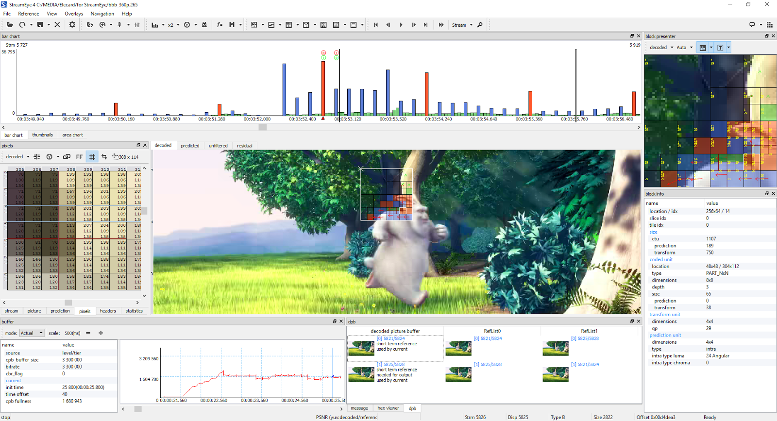
Screenshot of the open video in the program Elecard StreamEye , 1920 × 1040
Hardware support for encoding and decoding means that the processor implements integrated circuits that are specialized for specific encoding and decoding tasks. For example, the discrete cosine transform (DCT) is performed during encoding, and the inverse discrete cosine transform is performed during decoding.
Over the past five years, Intel QSV technology has progressed significantly. Added support for free VP8 and VP9 video codecs, updated drivers for Linux, etc.
The technology has improved with every new generation of Intel Core, right up to the current 6th generation Skylake.
The latest version of QSV 5.0 was released along with Skylake sixth generation microarchitecture. This version of the GPU in the official documentation of Intel is classified as Gen9, that is, the graphics of the 9th generation.

The Intel Core i7 6700K desktop processor contains 4 CPU cores and 9th generation HD Graphics 530 graphics
With each new micro-architecture in the GPU, the number of instruction execution blocks (EU) increased. It grew from 6 in Sandy Bridge to 72 in the top-end Iris Pro Graphics 580 on Skylake crystals. Including due to this, the performance of the GPU has increased tenfold without increasing the clock frequency. Throughout the latest generation of Iris and Iris Pro graphics, there is a built-in Level 4 cache of 64 or 128 MB.
The basic building block of the Gen9 microarchitecture is the command execution block (EU). Each EU combines simultaneous multithreading (SMT) and carefully tuned alternating multithreading (IMT). Here work arithmetic-logical devices with a single stream of commands, multiple data stream (SIMD ALU). They are built along pipelines of numerous threads for high-speed floating-point calculations and integer operations.
The essence of alternating multithreading in the EU is to ensure a continuous stream of instructions ready for execution, but at the same time to queue with a minimal delay more complex operations, such as placing vectors in memory, sampling requests or other system communications.

Command execution block (EU)
Each thread in the Gen9 command execution block contains 128 general-purpose registers. In each of the registers there are 32 bytes of memory available as an 8-element SIMD vector or 32-bit data elements. Thus, for each thread there are 4 KB of the general-purpose registry file (GRF). Only one EU accounts for 7 threads with a total of 28 KB GRF per EU. Flexible addressing system allows you to address multiple registers together. The thread state is currently stored in a separate registry architecture file (ARF).
Depending on the load, hardware threads in the EU can execute in parallel one code from one computational core or can execute code from completely different computational cores. The execution status in each thread, including its own instruction pointers, is stored in its independent ARF. On each cycle, the EU can issue up to four different instructions, which should be from four different threads. The Thread Arbiter (Special Arbiter) sends these instructions to one of the four function blocks for execution. Usually the arbiter can choose from disparate instructions to simultaneously load all the functional blocks and, thus, to ensure concurrency at the instruction level.
A pair of FPU modules in the circuit actually performs both floating point operations and integer calculations. In Gen9, these modules can handle for a cycle not only up to four operations with 32-bit numbers, but also up to eight operations with 16-bit ones. The operations of addition and multiplication are performed simultaneously, that is, the EU unit is capable of performing a maximum of 16 operations with 32-bit numbers per cycle: 2 FPUs of 4 operations × 2 (addition + multiplication).
The corresponding compilers, such as RenderScript, OpenCL, Microsoft DirectX Compute Shader, OpenGL Compute and C ++ AMP, are engaged in generating SPMD code for multi-threaded EU downloads. The compiler itself heuristically selects the thread loading mode (SIMD-width): SIMD-8, SIMD-16 or SIMD-32. Thus, in the case of SIMD-16, 112 (16 × 7) streams can be simultaneously executed on one EU.
Data exchange within a single instruction within an EU block can be, for example, 96 bytes for reading and 32 bytes for writing. When scaling to the entire GPU, taking into account several levels of the memory hierarchy, it turns out that the maximum theoretical limit of data exchange between FPU and GRF reaches several terabytes per second.
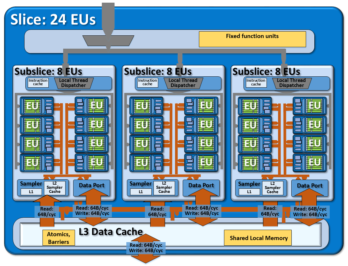
The GPU microarchitecture has scalability at all levels. Scalability at the thread level goes into scalability at the level of command execution blocks. In turn, these blocks of command execution will unite in groups of eight (8 EU = 1 subslice).
At each scale level, there are local modules that work only here. For example, each group of 8 EU blocks has its own local thread manager, a data port and a sampler for textures.

Group of 8 EU units (subslice)
In turn, groups of 8 EU are combined into groups of 24 EU (3 sublices = 1 slice). These sections of 24 blocks, in turn, are also scaled: the existing Gen9 graphics contains 24, 48 or 72 EU.
In the Gen9 graphics, the L3 third-level cache has been increased to 768 KB for each group of 24 EU. All samplers and data ports have their own L3 access interface, allowing you to read and write 64 bytes per cycle. Thus, a group of 24 EU has three data ports with a data bandwidth to the L3 cache of 192 bytes per cycle. If there is no data in the cache on request, then the data is requested or sent for writing to the system memory, also 64 bytes per cycle.

Gen9 microarchitecture from two groups of 24 (3 × 8) EU
This scalability allows you to effectively reduce power consumption by disabling those modules that are not involved at the moment.
Gen9 introduced full hardware acceleration support for H.265 / HEVC encoding and decoding , partial support for hardware encoding and decoding with the free VP9 codec. Significant improvements in QSV technology. They improved the quality and efficiency of encoding and decoding, as well as the performance of filters in transcoding and video editing programs that use hardware acceleration.
Skylake integrated graphics support DirectX 12 Feature Level 12_1, OpenGL 4.4 and OpenCL 2.0 standards. It was decided to completely abandon the VGA monitors, but Skylake GPUs support up to three monitors with HDMI 1.4, DisplayPort 1.2 or Embedded DisplayPort (eDP) 1.3 interfaces.
Hardware accelerated video decoding is available to the graphics driver via the Direct3D Video API (DXVA2), Direct3d11 Video API or Intel Media SDK interfaces, as well as through Media Foundation Transform MFT filters.
In Gen9 graphics, hardware accelerated decoding of AVC, VC1, MPEG2, HEVC (8 bits), VP8, VP9 and JPEG is supported.
Source: 6th Generation Intel Processor Datasheet for S-Platforms
Estimated video decoding performance with hardware acceleration is more than 16 simultaneous 1080p video streams. Actual performance depends on the GPU model, bit rate and clock frequency. H264 SVC hardware decoding is not supported in Skylake.
Hardware acceleration of coding is available only through the interfaces Intel Media SDK, as well as through MFT (Media Foundation Transform) filters.
Source: 6th Generation Intel Processor Datasheet for S-Platforms
In addition to hardware acceleration of encoding and decoding, Gen9 graphics hardware acceleration of video processing, including the following functions: deinterlacing, cadence detection, video scaling (Advanced Video Scaler), improved detail, image stabilization, gamma compression (gamut compression), adaptive HD contrast enhancement, skin tone enhancement, color control, noise reduction in the color component of the channel (chroma de-noise), SFC conversion (Scalar and Format Conversion), memory compression, LACE (Localized Adaptive Contrast Enhancement), space governmental noise reduction, Out-Of-Loop De-blocking (for AVC decoder), and others.
Gen9 hardware transcoder supports the following specific transcoding functions:
In terms of video analytics applications, Gen9 supports hardware acceleration for a range of filters that can be useful in applications like face recognition, facial expression recognition, gesture recognition, object tracking, etc. (see table).

Source: 6th Generation Intel Processor Datasheet for S-Platforms
Gen9 has implemented hardware support for processing video from digital cameras (Camera Processing Pipeline), including some of the processing features: white balance, full-color image recovery from an array of color filters on a camera sensor (de-mosaic), correction of defective pixels, black correction , gamma correction, elimination of vignetting, front end color space converter (CSC), image enhancement (Image Enhancement Color Processing, IECP).
Skylake gpu
To use hardware acceleration, each program must explicitly implement support for specific Gen9 functions. Many do it. Intel publishes the open source Media SDK 2.0 , so support for hardware accelerated encoding and decoding can be embedded in any program. In addition, there are ready-made applications for transcoding live video on Intel codecs, such as Elecard CodecWorks 990 . Unlike the SDK, CodecWorks 990 does not require the participation of programmers for use in real-world tasks, it already contains the most popular transcoding profiles, and the non-programmer as a whole is much easier to work with than the SDK. How hardware accelerated software transcoders work is described in the next section.
( To be continued ...)
Integrated graphics of the 9th generation HD Graphics 530 in an Intel Core i7 6700K processor with 24 instruction execution units (EU), organized in three fragments of 8 units.
Surprisingly, Intel has managed to circumvent both AMD and Nvidia in implementing video acceleration hardware acceleration: similar AMD Video Codec Engine and Nvidia NVENC technologies in AMD and Nvidia video cards appeared very late (compression algorithms require serious adaptation to video card processors). That is why the idea and development of QSV has been kept secret for five years .
To say that QSV was claimed is to say nothing. Reproduction (decoding) of video with hardware support has become much less to take away resources from other tasks in the OS, to heat up the CPU less and to consume less electricity.
')
In addition, in recent years, video encoding has become one of the most resource-intensive tasks on a PC. The popularity of YouTube has turned millions of people into cameramen and directors. And then there's the ubiquitous distribution of smartphones that require transcoding from DVD to compressed AVC MP4 / H.264. As a result, almost every PC has become a video studio. IPTV and streaming video broadcasts on the Internet have spread massively. The computer began to perform the role of the TV. The video became ubiquitous and turned into one of the most popular types of content on PC. It is encoded and transcoded constantly and everywhere: on different bit rates, depending on the type of device, screen size and Internet speed. In such a situation, the ability to quickly encode and decode video in the processors suggested itself. So in Intel GPU embedded hardware encoder / decoder.
A modern codec processes each frame separately, but also analyzes the sequence of frames for repetitions in time (between frames) and space (within one frame). This is a complex computational task. Below is an example of a frame from a video that is encoded with the latest HEVC codec. For a particular site near the ear of the hare, it is shown exactly how the various parts of the frame were encoded. It also shows the position and type of frame in the overall structure of the video stream. Without going into the details of the video compression algorithms, this gives a general idea of how much information is required to analyze in order to efficiently encode and decode video.
Screenshot of the open video in the program Elecard StreamEye , 1920 × 1040
Hardware support for encoding and decoding means that the processor implements integrated circuits that are specialized for specific encoding and decoding tasks. For example, the discrete cosine transform (DCT) is performed during encoding, and the inverse discrete cosine transform is performed during decoding.
Over the past five years, Intel QSV technology has progressed significantly. Added support for free VP8 and VP9 video codecs, updated drivers for Linux, etc.
The technology has improved with every new generation of Intel Core, right up to the current 6th generation Skylake.
9th generation GPU microarchitecture
The latest version of QSV 5.0 was released along with Skylake sixth generation microarchitecture. This version of the GPU in the official documentation of Intel is classified as Gen9, that is, the graphics of the 9th generation.
The Intel Core i7 6700K desktop processor contains 4 CPU cores and 9th generation HD Graphics 530 graphics
With each new micro-architecture in the GPU, the number of instruction execution blocks (EU) increased. It grew from 6 in Sandy Bridge to 72 in the top-end Iris Pro Graphics 580 on Skylake crystals. Including due to this, the performance of the GPU has increased tenfold without increasing the clock frequency. Throughout the latest generation of Iris and Iris Pro graphics, there is a built-in Level 4 cache of 64 or 128 MB.
▍ Micro-architecture of command execution blocks (EU)
The basic building block of the Gen9 microarchitecture is the command execution block (EU). Each EU combines simultaneous multithreading (SMT) and carefully tuned alternating multithreading (IMT). Here work arithmetic-logical devices with a single stream of commands, multiple data stream (SIMD ALU). They are built along pipelines of numerous threads for high-speed floating-point calculations and integer operations.
The essence of alternating multithreading in the EU is to ensure a continuous stream of instructions ready for execution, but at the same time to queue with a minimal delay more complex operations, such as placing vectors in memory, sampling requests or other system communications.
Command execution block (EU)
Each thread in the Gen9 command execution block contains 128 general-purpose registers. In each of the registers there are 32 bytes of memory available as an 8-element SIMD vector or 32-bit data elements. Thus, for each thread there are 4 KB of the general-purpose registry file (GRF). Only one EU accounts for 7 threads with a total of 28 KB GRF per EU. Flexible addressing system allows you to address multiple registers together. The thread state is currently stored in a separate registry architecture file (ARF).
Depending on the load, hardware threads in the EU can execute in parallel one code from one computational core or can execute code from completely different computational cores. The execution status in each thread, including its own instruction pointers, is stored in its independent ARF. On each cycle, the EU can issue up to four different instructions, which should be from four different threads. The Thread Arbiter (Special Arbiter) sends these instructions to one of the four function blocks for execution. Usually the arbiter can choose from disparate instructions to simultaneously load all the functional blocks and, thus, to ensure concurrency at the instruction level.
A pair of FPU modules in the circuit actually performs both floating point operations and integer calculations. In Gen9, these modules can handle for a cycle not only up to four operations with 32-bit numbers, but also up to eight operations with 16-bit ones. The operations of addition and multiplication are performed simultaneously, that is, the EU unit is capable of performing a maximum of 16 operations with 32-bit numbers per cycle: 2 FPUs of 4 operations × 2 (addition + multiplication).
The corresponding compilers, such as RenderScript, OpenCL, Microsoft DirectX Compute Shader, OpenGL Compute and C ++ AMP, are engaged in generating SPMD code for multi-threaded EU downloads. The compiler itself heuristically selects the thread loading mode (SIMD-width): SIMD-8, SIMD-16 or SIMD-32. Thus, in the case of SIMD-16, 112 (16 × 7) streams can be simultaneously executed on one EU.
Data exchange within a single instruction within an EU block can be, for example, 96 bytes for reading and 32 bytes for writing. When scaling to the entire GPU, taking into account several levels of the memory hierarchy, it turns out that the maximum theoretical limit of data exchange between FPU and GRF reaches several terabytes per second.
▍ Scalability
The GPU microarchitecture has scalability at all levels. Scalability at the thread level goes into scalability at the level of command execution blocks. In turn, these blocks of command execution will unite in groups of eight (8 EU = 1 subslice).
At each scale level, there are local modules that work only here. For example, each group of 8 EU blocks has its own local thread manager, a data port and a sampler for textures.
Group of 8 EU units (subslice)
In turn, groups of 8 EU are combined into groups of 24 EU (3 sublices = 1 slice). These sections of 24 blocks, in turn, are also scaled: the existing Gen9 graphics contains 24, 48 or 72 EU.
In the Gen9 graphics, the L3 third-level cache has been increased to 768 KB for each group of 24 EU. All samplers and data ports have their own L3 access interface, allowing you to read and write 64 bytes per cycle. Thus, a group of 24 EU has three data ports with a data bandwidth to the L3 cache of 192 bytes per cycle. If there is no data in the cache on request, then the data is requested or sent for writing to the system memory, also 64 bytes per cycle.
Gen9 microarchitecture from two groups of 24 (3 × 8) EU
This scalability allows you to effectively reduce power consumption by disabling those modules that are not involved at the moment.
What can QSV in Skylake
Gen9 introduced full hardware acceleration support for H.265 / HEVC encoding and decoding , partial support for hardware encoding and decoding with the free VP9 codec. Significant improvements in QSV technology. They improved the quality and efficiency of encoding and decoding, as well as the performance of filters in transcoding and video editing programs that use hardware acceleration.
Skylake integrated graphics support DirectX 12 Feature Level 12_1, OpenGL 4.4 and OpenCL 2.0 standards. It was decided to completely abandon the VGA monitors, but Skylake GPUs support up to three monitors with HDMI 1.4, DisplayPort 1.2 or Embedded DisplayPort (eDP) 1.3 interfaces.
Hardware accelerated video decoding is available to the graphics driver via the Direct3D Video API (DXVA2), Direct3d11 Video API or Intel Media SDK interfaces, as well as through Media Foundation Transform MFT filters.
In Gen9 graphics, hardware accelerated decoding of AVC, VC1, MPEG2, HEVC (8 bits), VP8, VP9 and JPEG is supported.
▍ Hardware Video Decoding Acceleration
| Codec | Profile | Level | Maximum resolution |
| MPEG2 | Main | Main High | 1080p |
| VC1 / WMV9 | Advanced Main Simple | L3 High Simple | 3840 × 3840 |
| AVC / H264 | High Main MVC & stereo | L5.1 | 2160p (4K) |
| VP8 | 0 | Unified level | 1080p |
| JPEG / MJPEG | Baseline | Unified level | 16k × 16k |
| HEVC / H265 | Main | L5.1 | 2160 (4K) |
| VP9 | 0 (4: 2: 0 Chroma 8-bit) | Unified level | ULT, 4k 24fps @ 15Mbps ULX, 1080p 30fps @ 10Mbps |
Estimated video decoding performance with hardware acceleration is more than 16 simultaneous 1080p video streams. Actual performance depends on the GPU model, bit rate and clock frequency. H264 SVC hardware decoding is not supported in Skylake.
Hardware acceleration of coding is available only through the interfaces Intel Media SDK, as well as through MFT (Media Foundation Transform) filters.
▍ Hardware Video Coding Acceleration
| Codec | Profile | Level | Maximum resolution |
| MPEG2 | Main | High | 1080p |
| AVC / H264 | Main High | L5.1 | 2160p (4K) |
| VP8 | Unified profile | Unified level | - |
| Jpeg | Baseline | - | 16K × 16K |
| HEVC / H265 | Main | L5.1 | 2160p (4K) |
| VP9 | 8-bit 4: 2: 0 BT2020 | - | - |
In addition to hardware acceleration of encoding and decoding, Gen9 graphics hardware acceleration of video processing, including the following functions: deinterlacing, cadence detection, video scaling (Advanced Video Scaler), improved detail, image stabilization, gamma compression (gamut compression), adaptive HD contrast enhancement, skin tone enhancement, color control, noise reduction in the color component of the channel (chroma de-noise), SFC conversion (Scalar and Format Conversion), memory compression, LACE (Localized Adaptive Contrast Enhancement), space governmental noise reduction, Out-Of-Loop De-blocking (for AVC decoder), and others.
Gen9 hardware transcoder supports the following specific transcoding functions:
- Fast and energy efficient AVC encoder for video conferencing
- Lossless memory compression for a media stick to reduce power consumption
- Video Scaling (Advanced Video Scaler)
- Energy efficient SFC converter (Scalar and Format Conversion)
In terms of video analytics applications, Gen9 supports hardware acceleration for a range of filters that can be useful in applications like face recognition, facial expression recognition, gesture recognition, object tracking, etc. (see table).
Source: 6th Generation Intel Processor Datasheet for S-Platforms
Gen9 has implemented hardware support for processing video from digital cameras (Camera Processing Pipeline), including some of the processing features: white balance, full-color image recovery from an array of color filters on a camera sensor (de-mosaic), correction of defective pixels, black correction , gamma correction, elimination of vignetting, front end color space converter (CSC), image enhancement (Image Enhancement Color Processing, IECP).
Skylake gpu
- HD Graphics 510 (GT1, 12 EU, 950 MHz, 182.4 Gflops)
- HD Graphics 515 (GT2, 24 EU, 1000 MHz, 384 Gflops)
- HD Graphics 520 (GT2, 24 EU, 1050 MHz, 403.2 Gflops)
- HD Graphics 530 (GT2, 24 EU, 1150 MHz, 441.6 Gflops)
- Iris Graphics 540 (GT3e, 48 EU, 64 MB eDRAM, 1050 MHz, 806.4 Gflops)
- Iris Graphics 550 (GT3e, 48 EU, 64 MB eDRAM, 1100 MHz, 844.8 Gflops)
- Iris Pro Graphics 580 (GT4e, 72 EU, 128 MB eDRAM, 1000 MHz, 1152 Gflops)
- HD Graphics P530 server (GT2, 24 EU, 1150 MHz, 441.6 Gflops)
- Iris Pro Graphics P555, server (GT3e, 48 EU, 128 MB eDRAM, 1000 MHz, 768 Gflops)
- Iris Pro Graphics P580, server (GT4e, 72 EU, 128 MB eDRAM, 1000 MHz, 1152 Gflops)
How programs use hardware acceleration
To use hardware acceleration, each program must explicitly implement support for specific Gen9 functions. Many do it. Intel publishes the open source Media SDK 2.0 , so support for hardware accelerated encoding and decoding can be embedded in any program. In addition, there are ready-made applications for transcoding live video on Intel codecs, such as Elecard CodecWorks 990 . Unlike the SDK, CodecWorks 990 does not require the participation of programmers for use in real-world tasks, it already contains the most popular transcoding profiles, and the non-programmer as a whole is much easier to work with than the SDK. How hardware accelerated software transcoders work is described in the next section.
( To be continued ...)
Source: https://habr.com/ru/post/311320/
All Articles