Useful properties of jitter
Jitter is the jitter of the clock signal. The less jitter the better. Large jitter affects the ADC parameters, worsens the FPGA trace. However, there are situations when jitter is useful. For example, it can be used for automatic adjustment of the clock frequency.
Let's consider the classic task of connecting an ADC over a parallel bus.
In general, the connection diagram looks like this:
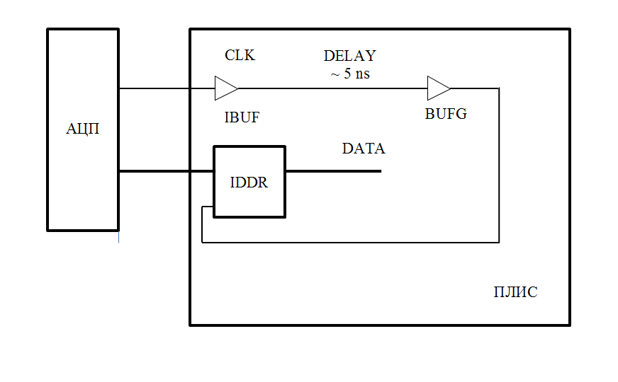
The ADC data bus enters the FPGAs, a DDR trigger or deserializer is located directly inside the I / O unit, and then the data is sent to the FIFO via a parallel bus. The problem is the passage of the clock signal. If you use a global buffer, then the signal propagation time to the buffer and back can be 5 ns. This is a lot. This is comparable to the period of the clock frequency, which can easily be 200-500 MHz.
A few words why this is bad. In general, the ADC should operate in a certain frequency range. Consider, for example, a situation with a clock delay of 2.8 ns, with a clock frequency of 500 MHz.
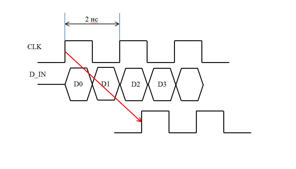
At first glance, everything is fine, the ADC data snap perfectly. But what will happen if the frequency is reduced to 357 MHz, it will be just 2.8 ns?
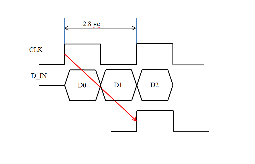
Data travels to the front and we get data corruption. With a further decrease in frequency, the hitting will disappear and the data will again be correct.
There are two classic ways to solve a problem:
')
1. In the IOB block there is a delay element, it can set a delay of up to 2.4 ns. In most cases this is enough.
2. There are special elements bufio, through them the clock frequency path becomes much shorter.
Unfortunately, this is not always enough. The delay may exceed 2.4 ns, especially on large FPGAs. And not always the clock signal is brought to the output of bufio.
There is a simple and elegant solution to this problem. To do this, it is enough to make it so that the phase of the internal clock signal always exactly coincides with the phase of the ADC clock signal. The existing DCM, MMCM, or PLL nodes inside the FPGA are able to smoothly change the phase. But the sensor can serve as a D-trigger inside the IOB block. Here is the wiring diagram:
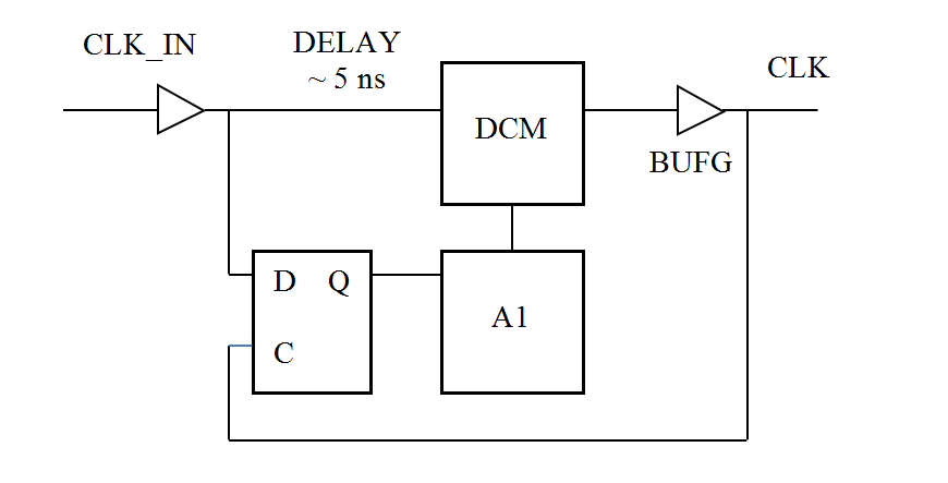
The input clock signal passes through the IOB and is fed to the DCM input, at the same time it is fed to the input of the D-flip-flop. The D-flip-flop clock input receives a signal after DCM, the same signal goes to the ADC data bus triggers. And that's what happens, consider a few situations:
Situation 1 - the front of the global signal is significantly to the left of the front of the input signal. At the exit of the trigger - zeros.
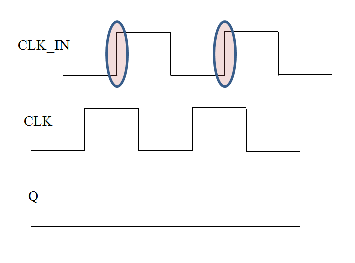
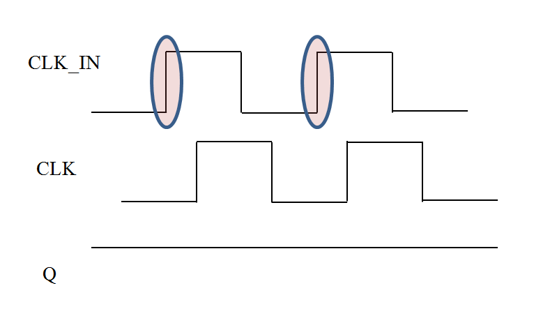
Situation 2 - the front of the global signal in the jitter zone. The output is a random sequence. This is the very useful property of jitter. By the occurrence of a random sequence, you can determine the fact of the adjustment of the clock frequency.
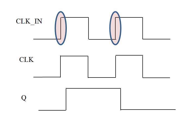
Situation 3 - the front of the global signal is significantly to the right of the input signal. At the exit - units.
All these situations are easily handled by the state machine. In my implementation, there is an accumulation cycle, in the course of 1024 cycles, the counting is performed 1. If the counter value is greater than 576, then the phase shift to the left is performed. If the counter value is less than 448, then a phase shift to the right occurs.
The figure shows the result of modeling the component.
It can be seen that after adjustment there is a small oscillatory process - a shift within one value. In real systems in the steady state, a phase change within one or two readings is also observed. Before the start of the adjustment was as follows:
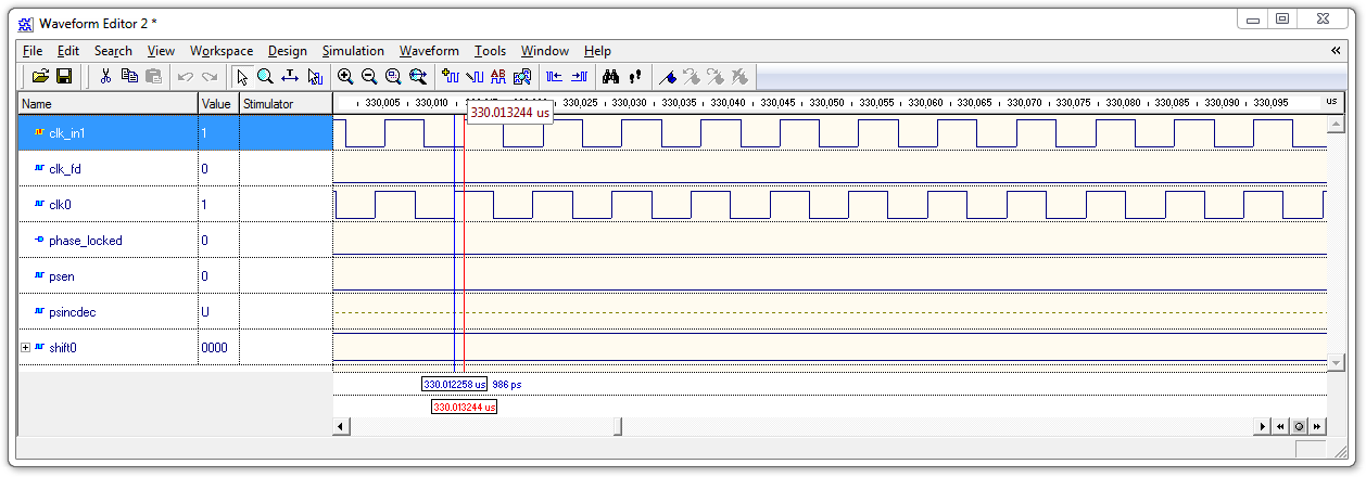
It is seen that there is a large offset between the frequencies. And after adjustment like this:
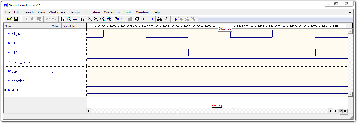
The frequencies are the same.
»Finished components are presented on GitHub :
I laid out two components:
A few words about the modeling. Since it is based on a random process, this creates some problems. But they are solvable. In the stand, the model_line_v1 component is used, which just generates jitter on the clock signal. To generate jitter, use the UNIFORM function from the math_real library.
In conclusion, I want to note that these components are used in many of our projects. And they help us a lot.
Let's consider the classic task of connecting an ADC over a parallel bus.
In general, the connection diagram looks like this:
The ADC data bus enters the FPGAs, a DDR trigger or deserializer is located directly inside the I / O unit, and then the data is sent to the FIFO via a parallel bus. The problem is the passage of the clock signal. If you use a global buffer, then the signal propagation time to the buffer and back can be 5 ns. This is a lot. This is comparable to the period of the clock frequency, which can easily be 200-500 MHz.
A few words why this is bad. In general, the ADC should operate in a certain frequency range. Consider, for example, a situation with a clock delay of 2.8 ns, with a clock frequency of 500 MHz.
At first glance, everything is fine, the ADC data snap perfectly. But what will happen if the frequency is reduced to 357 MHz, it will be just 2.8 ns?
Data travels to the front and we get data corruption. With a further decrease in frequency, the hitting will disappear and the data will again be correct.
There are two classic ways to solve a problem:
')
1. In the IOB block there is a delay element, it can set a delay of up to 2.4 ns. In most cases this is enough.
2. There are special elements bufio, through them the clock frequency path becomes much shorter.
Unfortunately, this is not always enough. The delay may exceed 2.4 ns, especially on large FPGAs. And not always the clock signal is brought to the output of bufio.
There is a simple and elegant solution to this problem. To do this, it is enough to make it so that the phase of the internal clock signal always exactly coincides with the phase of the ADC clock signal. The existing DCM, MMCM, or PLL nodes inside the FPGA are able to smoothly change the phase. But the sensor can serve as a D-trigger inside the IOB block. Here is the wiring diagram:
The input clock signal passes through the IOB and is fed to the DCM input, at the same time it is fed to the input of the D-flip-flop. The D-flip-flop clock input receives a signal after DCM, the same signal goes to the ADC data bus triggers. And that's what happens, consider a few situations:
Situation 1 - the front of the global signal is significantly to the left of the front of the input signal. At the exit of the trigger - zeros.
Situation 2 - the front of the global signal in the jitter zone. The output is a random sequence. This is the very useful property of jitter. By the occurrence of a random sequence, you can determine the fact of the adjustment of the clock frequency.
Situation 3 - the front of the global signal is significantly to the right of the input signal. At the exit - units.
All these situations are easily handled by the state machine. In my implementation, there is an accumulation cycle, in the course of 1024 cycles, the counting is performed 1. If the counter value is greater than 576, then the phase shift to the left is performed. If the counter value is less than 448, then a phase shift to the right occurs.
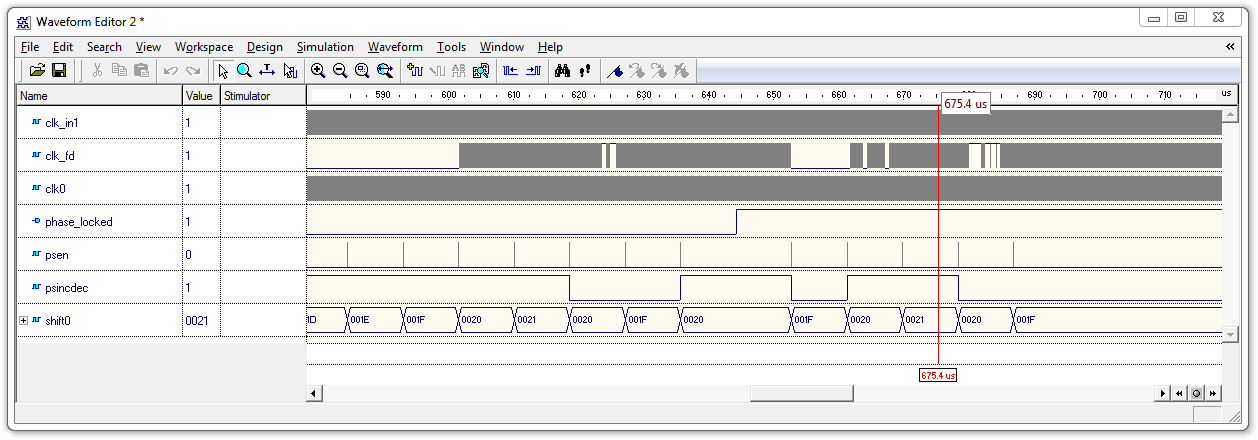
The figure shows the result of modeling the component.
The clk_in1 signal is an input clock.
clk0 - tuned frequency
clk_fd - phase detector
The signal phase_locked = 1 means that the phase adjustment has been reached.
psen - DCM phase shift
psincdec - phase shift direction
shift0 - the current value of the phase counter
It can be seen that after adjustment there is a small oscillatory process - a shift within one value. In real systems in the steady state, a phase change within one or two readings is also observed. Before the start of the adjustment was as follows:
It is seen that there is a large offset between the frequencies. And after adjustment like this:
The frequencies are the same.
»Finished components are presented on GitHub :
I laid out two components:
ctrl_dcm_phase_v6 –DCM is installed internally. This is for Spartan 3, Virtex 4, Virtex 5
ctrl_dcm_phase_v8 - external DCM or MMCM, this is for Virtex 6, Kintex 7.
A few words about the modeling. Since it is based on a random process, this creates some problems. But they are solvable. In the stand, the model_line_v1 component is used, which just generates jitter on the clock signal. To generate jitter, use the UNIFORM function from the math_real library.
In conclusion, I want to note that these components are used in many of our projects. And they help us a lot.
Source: https://habr.com/ru/post/309944/
All Articles