Modern art on the screen of a hardware company engineer
Hello! My name is Maxim, I work as an engineer in one company. The company makes servers and other hardware on the POWER-architecture (which one and why is this - others will tell later), but for now I want to show a section of the server's motherboard - this is my area of responsibility.
In general, there will be something like a work log (worklog), together with colleagues we will post stories about the origin of life in pieces of iron. First, about the server, and then about the rest.
How best to put voltage converters here?
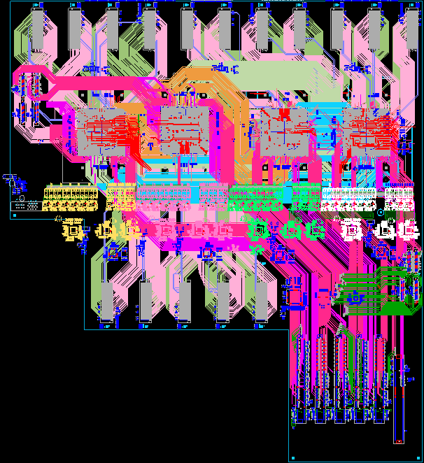
The above screen is not the result of the artist's hallucinations, creating in the style of POP-ART, but the motherboard on which four groups of voltage converters need to fit — one for each processor (yellow, pink, bright green and white in the screenshot).
')
At first they wanted to bring them to external boards, as in the figure below:

Initial idea for converter placement
According to the original idea, each board had to carry VRMs for two processors and associated memory modules. But after elaboration, they decided to abandon this option - a wildly high current requires a large CardEdge-connector, which will make the interprocessor bus tracing more difficult.
Now try to sip VRMs on the motherboard. This also complicates tracing - now high-speed tires, because You will have to change the location of the tracks in order to bend around the vias (vias), which are necessary for applying voltages to the processors from the converters. And you need a lot of holes! For processors and memory modules, a large current is needed, and the density of this current passing through vias should be minimized. If you save on the number of vias, it will cause them to overheat (due to the high current density) and degrade with time until they burn out.

Almost a screenshot of TRON 2.0, I want to cry in bloody tears. The holes are highlighted in yellow - in fact, this is a highlighting of errors due to the intersection of the tracks of different tires with them. We need to take all these tracks to the side.
In general, the complexity of the project within my tasks lies in the fact that it is necessary to trace on the board, in addition to power buses with high current (up to 250 A!), Many high-speed buses - PCIe Gen3 (8 Gbps), DMI (9.6 Gbps, Differential Memory Interface , bus of connection of Centaur memory buffer chips), A-bus interprocessor buses (6.4 Gbps, SMP link).
There are also a lot of components - 4 processors, 16 connectors for DDR4 riser memory cards, a total of 14 connectors for PCIe (of which 8 are NanoPitch , and 6 are regular connectors for expansion cards), and the installation is very tight. The first screen gives a sufficient idea of the scale of the trouble - this is a simplified image with a fair amount of components hidden from showing, so that an already dense picture does not overload.

The area between the two processors. It was possible to lay the paths between them very tightly.
Many high-speed interfaces - many restrictions. We have to strictly observe the requirements for routing - the maximum length, static and dynamic phases in differential pairs; the distance between diff pairs; maximum variation in length in the group, wave resistance, etc.
This, in turn, imposes restrictions on the bus routes on the board, the choice of material for the printed circuit board (material with low losses), the number of layers, etc.
Now we have a stack with 28 layers - 4 layers of them are allocated for the power bus, to increase the area of the power supply polygons - this minimizes IR drop (voltage drop on the conductor). We want not to exceed this number of layers, and I think we should do it.
In general, such here are working days. You get used to looking at such schemes with a close look - and then you notice that they are in their own way even artistic, like a mixture of lines and color spots of various shapes and shades. And the very trace of such a scale is an art in itself.
Finally I want to show another screen that hides the whole story:

This is not the coming of Cthulhu from the depths of the sea.
Due to the location of the memory slots, one processor had to be rotated 180 degrees. Why it was impossible to arrange the memory connectors otherwise? This is the story of the next series and I will not be a hero in it.
In general, there will be something like a work log (worklog), together with colleagues we will post stories about the origin of life in pieces of iron. First, about the server, and then about the rest.
How best to put voltage converters here?
The above screen is not the result of the artist's hallucinations, creating in the style of POP-ART, but the motherboard on which four groups of voltage converters need to fit — one for each processor (yellow, pink, bright green and white in the screenshot).
')
At first they wanted to bring them to external boards, as in the figure below:
Initial idea for converter placement
According to the original idea, each board had to carry VRMs for two processors and associated memory modules. But after elaboration, they decided to abandon this option - a wildly high current requires a large CardEdge-connector, which will make the interprocessor bus tracing more difficult.
Now try to sip VRMs on the motherboard. This also complicates tracing - now high-speed tires, because You will have to change the location of the tracks in order to bend around the vias (vias), which are necessary for applying voltages to the processors from the converters. And you need a lot of holes! For processors and memory modules, a large current is needed, and the density of this current passing through vias should be minimized. If you save on the number of vias, it will cause them to overheat (due to the high current density) and degrade with time until they burn out.
Almost a screenshot of TRON 2.0, I want to cry in bloody tears. The holes are highlighted in yellow - in fact, this is a highlighting of errors due to the intersection of the tracks of different tires with them. We need to take all these tracks to the side.
In general, the complexity of the project within my tasks lies in the fact that it is necessary to trace on the board, in addition to power buses with high current (up to 250 A!), Many high-speed buses - PCIe Gen3 (8 Gbps), DMI (9.6 Gbps, Differential Memory Interface , bus of connection of Centaur memory buffer chips), A-bus interprocessor buses (6.4 Gbps, SMP link).
A couple of words about A-Bus and Centaurs
A-Bus is one of the two interprocess communication buses on the POWER8. As for the Centaurs - IBM decided to remove the memory buffer into a separate chip when POWER8 was released. He also implements the L4 cache, is responsible for all logic, etc., conceived including. for a painless transition from DDR3 to DDR4.
If interested, you can write about them separately.
If interested, you can write about them separately.
There are also a lot of components - 4 processors, 16 connectors for DDR4 riser memory cards, a total of 14 connectors for PCIe (of which 8 are NanoPitch , and 6 are regular connectors for expansion cards), and the installation is very tight. The first screen gives a sufficient idea of the scale of the trouble - this is a simplified image with a fair amount of components hidden from showing, so that an already dense picture does not overload.
The area between the two processors. It was possible to lay the paths between them very tightly.
Many high-speed interfaces - many restrictions. We have to strictly observe the requirements for routing - the maximum length, static and dynamic phases in differential pairs; the distance between diff pairs; maximum variation in length in the group, wave resistance, etc.
This, in turn, imposes restrictions on the bus routes on the board, the choice of material for the printed circuit board (material with low losses), the number of layers, etc.
Now we have a stack with 28 layers - 4 layers of them are allocated for the power bus, to increase the area of the power supply polygons - this minimizes IR drop (voltage drop on the conductor). We want not to exceed this number of layers, and I think we should do it.
What is harmful IR drop
The phenomenon of IR drop, in addition to the actual problems with the drawdown of the supply voltage of the components, is also closely related to heat dissipation. The greater the voltage drop on the resistive line - the more energy goes into heat and overheating. In general, we strive to reduce this effect due to geometry. Here is a good article about IR drop and analysis of the phenomenon, depending on the form of the conductor - it clearly shows that the effect is reduced on wide ranges of food.
In general, such here are working days. You get used to looking at such schemes with a close look - and then you notice that they are in their own way even artistic, like a mixture of lines and color spots of various shapes and shades. And the very trace of such a scale is an art in itself.
Finally I want to show another screen that hides the whole story:
This is not the coming of Cthulhu from the depths of the sea.
Due to the location of the memory slots, one processor had to be rotated 180 degrees. Why it was impossible to arrange the memory connectors otherwise? This is the story of the next series and I will not be a hero in it.
Source: https://habr.com/ru/post/308508/
All Articles