Work with radio modules SI4432
The article describes the functional features of the radio module on the ISM chip (industrial, scientific and medical radio bands) of the SI4432 transceiver. It also provides the simplest examples of software initialization of the module and describes some possible configuration variations.
Receiver sensitivity -121 dBm . Transmitter power up to +20 dBm (software tuning is possible in 3 dBm increments). There is a built-in function of separated reception (Antenna Diversity) . The microcircuit is capable of operating at frequencies from 240 to 960 MHz in increments of 156 (240-480 MHz) or 312 Hz (480-960 MHz). Also, the chip has such features as: automatic wake-up timer, low battery charge detector, 64-byte receive / transmit buffer, automatic packet handler, temperature sensor, 8-bit ADC, reference voltage source, three GPIO outputs, various types of signal modulation (OOK, FSK, GFSK) and others.
The microcircuit runs from 1.8 to 3.6 V of the supply voltage.
')
There are no voltage regulators on the module, so you need the appropriate power supply and the appropriate level at the logic inputs. On the module, one more small six-lead chip with G4C marking is visible. This is the uPG2179TB chip, which performs the function of switching the antenna between the TX and RX terminals, thus ensuring that the module can operate in both receive mode and transmit mode. The switch chip is controlled by the SI4432 itself through the ports GPIO0 and GPIO1, which, when initialized, must be programmed accordingly, to change / set the receive / transmit mode. At the same time, this circuit configuration does not allow using the diversity reception function, and the operation of the GPIO0 and GPIO1 pins should be assigned only to control the uPG2179TB switch.
The values of the capacitors and inductances installed in the piping of the antenna inputs of the SI4432 should be selected based on the operating frequency range, antenna characteristics and supply voltage range. What particular values have these elements is unknown.
The scheme of the module, namely the one shown in the figure I did not find, but according to the information from the datasheet, you can install the pinout of the module:
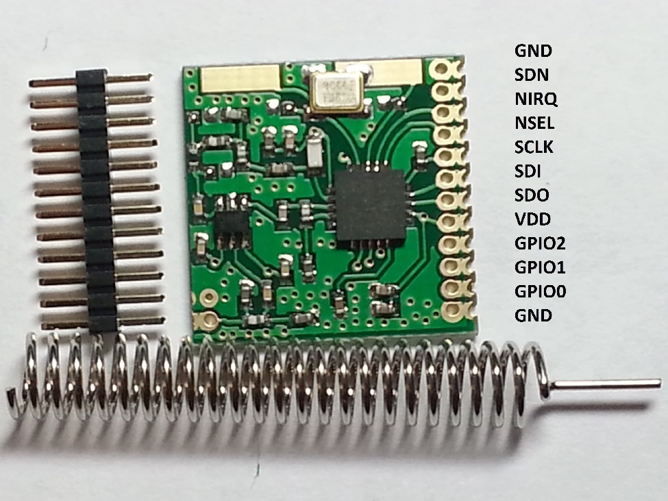
NSEL, SCLK, SDI, SDO - SPI interface (working with SI4432 comes down to writing and reading SI4432 registers via SPI interface);
NIRQ - output interrupts (if a receive / transmit event occurs, etc., then the level at this output drops to 0, which events will lead to interrupts depending on the values of the bits in the corresponding registers);
SDN - output control mode of the SI4432, if you set a high level to SDN, then the SI4432 switches to Shutdown mode, in which the chip goes to power saving mode with a current consumption of 15 nA, while all the contents of the registers return to their original state and SPI data transmission is impossible ;
VDD - module power supply from 1.8 to 3.6 V;
GND - the "land";
GPIO0, GPIO1, GPIO2 - programmable input / output ports (if you do not rewire the module, then only GPIO2 can be programmed for your goals, since GPIO0 GPIO1 is already occupied to switch the transmit / receive mode).
All register settings described below are taken from the AN415 Programming guide . This file covers the use of the SI4432 as a transmitter, receiver, transceiver, and also deals with the transmission of packets with a length of more than 64 KB.
SI4432 chips come in different revisions: A, V, B. It is determined by the first letter in the cipher, in my case BPS10P, which means revision B. For different revisions there are some features in the initialization.
The module connection is made in accordance with the pinout above. For simple reception or transmission of data, GPIO pins can be turned off at the inputs of the microcontroller and leave them hanging in the air. The SPI pins are connected to the corresponding pins of the microcontroller, the NIRQ can be hung on any free pins of the microcontroller (probably better at such a pin where you can get an external interrupt on the front). SDN can be brought to the "ground" or to the output of the MK, but do not forget to set it to 0.
Manufacturer SI4432 offers to use the following functions for reading and writing registers for SPI.
Record:
Reading:
It is recommended to make the following manipulations.
1) Set the SDN pin to 0.
2) Wait 15 ms before sending commands via SPI.
3) Read the status of the interrupt registers.
4) Perform a soft reset.
Reading statuses clears the interrupt flags and resets the NIRQ output to 1 (when an interrupt occurs, the NIRQ is reset to 0 and remains in this state until the corresponding status register is read).
Since the microcircuit supports operation in a rather wide frequency range, configuring the registers responsible for the frequency is rather difficult. The manufacturer suggests using a calculator ( EZRadioPRO Register Calculator ) to calculate the values of frequency registers. The calculator is a Microsoft Excell file:
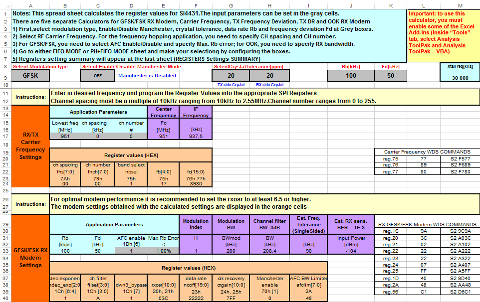
This file already has the appropriate default values. Values can only be changed in gray cells. It is advisable to change the value of the cells responsible for the transmission rate (J9) and the carrier frequency (B17) in this file. Usually, the slower the transmission rate, the lower the probability of an error occurring during data transfer. You can select the type of signal modulation: FSK, GFSK, OOK.
OOK modulation encodes the data by turning the signal amplifier on or off. When there is no data to transmit, the amplifier is disabled, when transmitting a logical 0, the amplifier is turned off for the duration of one bit, while transmitting a logical 1, the amplifier is turned on for the duration of one bit.
FSK is based on changing the frequency of a signal for transmitting digital data. For transmission of logical 0, the frequency of the carrier signal is reduced by the frequency of the deviation, and for logical 1, it increases. The difference between GFSK and FSK is that GFSK applies a Gaussian filter to the data bits.
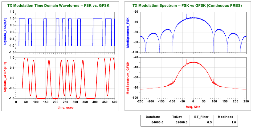
The manufacturer recommends using the GFSK type, since this type of modulation provides the best performance and a cleaner signal spectrum compared to other types of modulations available, as can be seen from the figure (comparing FSK and GFSK):
Configuring the registers responsible for the frequency:
The packet handler is used in receive mode and in transmit mode. You can transfer data without a packet handler, in which case you need to describe the structure of the packet in the registers yourself. Usually the structure of the package is as follows:
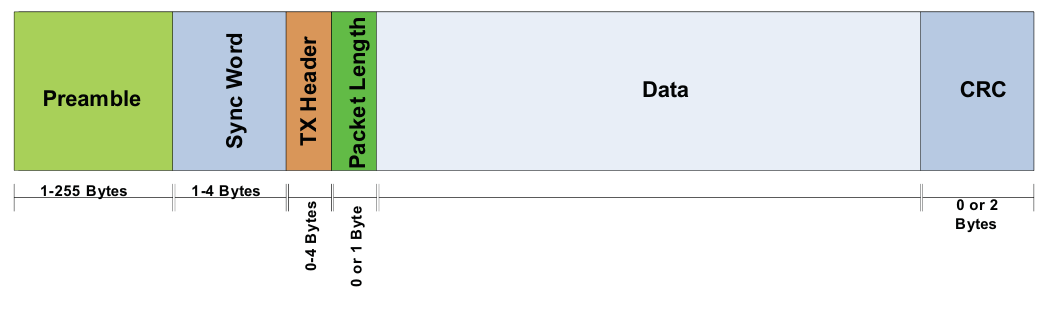
Preamble - sequence 0101 ... used to synchronize the receiver and transmitter. The SI4432 has an integrated preamble detector. When setting the SI4432 in registers, the value of the preamble length and the threshold value of the preamble detection are set. If the length of the preamble or the detection threshold of the preamble is less than a certain value, then the probability of loss of data packets will increase. The preamble detector searches for the preamble according to the detection threshold. If the corresponding preamble is found, then the synchronization word detection mechanism (Sync Word) is launched.
A transmitted packet always starts with a preamble (010101 ... bit pattern), which allows the receiver to prepare to receive transmitted data. The preamble dina, as well as the threshold, depend on the radio settings: modulation type, automatic frequency control (AFC). The SI4432 has a built-in preamble detector that automatically compares the bits received from the ether with the preamble bit pattern, if the preamble detector detects a predetermined length of the preamble bit sequence in the received signal, then SI4432 reports the reception of a valid preamble in the status register or the output of the GPIO if the corresponding GPIO setting.
Preamble detection threshold - programmable value. Depending on the modulation type (FSK, GFSK, OOK), enabling automatic frequency tuning (AFC) and diversity reception (antenna diversity), the manufacturer recommends choosing the preamble length and preamble detection threshold in accordance with the table:

After successfully detecting the preamble, the radio waits for a word of synchronization. On his arrival compares the received bits. After a successful comparison, the SI4432 begins to fill in the FIFO with the transmitted data. The synchronization word, known for the receiver and transmitter of the bit sequence, makes it possible to identify the transmitted data.
If the transmitted data has an arbitrary length (you can make a fixed one), then a byte with information about the length of the transmitted data is added to the packet.
A CRC checksum is also added to the packet.
Using the packet handler, the microcontroller configures the format of the transmitted packet once during initial setup of the SI4432, then, in order to transfer the data, the microcontroller must simply write it to the corresponding FIFO register SI4432.
Disabling the header, setting a variable number of bytes of the transmitted data (the number of transmitted bytes is recorded automatically in the transmitted data packet) and 2 bytes for the synchronization word:
Direct installation of sync word 0x2DD4:
Enable transmitter and CRC packet handler:
Selecting the FIFO modulation source and installing GFSK modulation:
The modulation source is the data that needs to be modulated to be broadcast. In this case, the FIFO is set by the source. But there is a direct mode when the data bits, with a certain timing, are fed to any output of the SI4432 (GPIOn, SDI, NIRQ).
As described earlier, the module has one output for the antenna and a mode switch for receiving transmission on the uPG2179TB chip, the outputs of which are connected to GPIO0 and GPIO1. Thus, it is possible to program the GPIO to automatically switch:
The accuracy of the center frequency setting is determined by the accuracy of the quartz resonator, its load capacity, as well as the various parasitic capacitances in the resonator circuit. To reduce the influence of these factors on the accuracy of the center frequency setting is possible in the following ways:
1) Use a higher deviation frequency for the transmitter and a wider range for the receiver.
2) Use AFC (Auto-frequency calibration), for this you need to increase the length of the preamble.
3) Adjust the register responsible for the load capacity of the quartz resonator:
We will send the package once a second.
Initialization of the receiver is similar to transmitter initialization. You must reset and read the status registers.
Radio parameters: 9.6 kbps, GFSK modulation, 45 kHz frequency deviation, 112.1 kHz receiving range. In accordance with the frequency calculator, the following registers are filled:
Similar to the transmitter: disabling the header, setting a variable number of bytes of the transmitted data (the number of transmitted bytes is recorded automatically in the transmitted data packet) and 2 bytes for the synchronization word:
Turn off header filtering:
Direct installation of sync word 0x2DD4:
Enable receiver receiver and CRC handler:
Enabling FIFO and GFSK modulation:
Setting the preamble detection threshold of 20 bits:
Setting the GPIO to automatically switch the antenna:
If the diversity reception is not used, the SGI bit in the AGC register must be set for the analog gain control to work correctly:
Setting the register responsible for the load capacity of the quartz resonator:
Receiver activation:
We enable two interrupts:
1) interrupt on receiving a valid packet;
2) CRC error interrupt.
Reading status registers to reset interrupts:
Main loop:
All information on programming modules is taken from the Application Note 415 Programming guide .
The datasheet on the SI4432 has a list of all Application Note, representing something like the peace reports related to the work of the SI4432. In addition to the datasheet and the specified Programming guide, there is one more useful document among Application Note - the register map . The programming guide also describes how to configure the transmitter for two-way communication. The register map provides a detailed description of all registers, modes of operation, and settings.
Description of the chip SI4432
Receiver sensitivity -121 dBm . Transmitter power up to +20 dBm (software tuning is possible in 3 dBm increments). There is a built-in function of separated reception (Antenna Diversity) . The microcircuit is capable of operating at frequencies from 240 to 960 MHz in increments of 156 (240-480 MHz) or 312 Hz (480-960 MHz). Also, the chip has such features as: automatic wake-up timer, low battery charge detector, 64-byte receive / transmit buffer, automatic packet handler, temperature sensor, 8-bit ADC, reference voltage source, three GPIO outputs, various types of signal modulation (OOK, FSK, GFSK) and others.
The microcircuit runs from 1.8 to 3.6 V of the supply voltage.
')
Features of the radio module
There are no voltage regulators on the module, so you need the appropriate power supply and the appropriate level at the logic inputs. On the module, one more small six-lead chip with G4C marking is visible. This is the uPG2179TB chip, which performs the function of switching the antenna between the TX and RX terminals, thus ensuring that the module can operate in both receive mode and transmit mode. The switch chip is controlled by the SI4432 itself through the ports GPIO0 and GPIO1, which, when initialized, must be programmed accordingly, to change / set the receive / transmit mode. At the same time, this circuit configuration does not allow using the diversity reception function, and the operation of the GPIO0 and GPIO1 pins should be assigned only to control the uPG2179TB switch.
The values of the capacitors and inductances installed in the piping of the antenna inputs of the SI4432 should be selected based on the operating frequency range, antenna characteristics and supply voltage range. What particular values have these elements is unknown.
The scheme of the module, namely the one shown in the figure I did not find, but according to the information from the datasheet, you can install the pinout of the module:
NSEL, SCLK, SDI, SDO - SPI interface (working with SI4432 comes down to writing and reading SI4432 registers via SPI interface);
NIRQ - output interrupts (if a receive / transmit event occurs, etc., then the level at this output drops to 0, which events will lead to interrupts depending on the values of the bits in the corresponding registers);
SDN - output control mode of the SI4432, if you set a high level to SDN, then the SI4432 switches to Shutdown mode, in which the chip goes to power saving mode with a current consumption of 15 nA, while all the contents of the registers return to their original state and SPI data transmission is impossible ;
VDD - module power supply from 1.8 to 3.6 V;
GND - the "land";
GPIO0, GPIO1, GPIO2 - programmable input / output ports (if you do not rewire the module, then only GPIO2 can be programmed for your goals, since GPIO0 GPIO1 is already occupied to switch the transmit / receive mode).
Module setup
All register settings described below are taken from the AN415 Programming guide . This file covers the use of the SI4432 as a transmitter, receiver, transceiver, and also deals with the transmission of packets with a length of more than 64 KB.
SI4432 chips come in different revisions: A, V, B. It is determined by the first letter in the cipher, in my case BPS10P, which means revision B. For different revisions there are some features in the initialization.
Connection to the controller
The module connection is made in accordance with the pinout above. For simple reception or transmission of data, GPIO pins can be turned off at the inputs of the microcontroller and leave them hanging in the air. The SPI pins are connected to the corresponding pins of the microcontroller, the NIRQ can be hung on any free pins of the microcontroller (probably better at such a pin where you can get an external interrupt on the front). SDN can be brought to the "ground" or to the output of the MK, but do not forget to set it to 0.
SPI Read and Write
Manufacturer SI4432 offers to use the following functions for reading and writing registers for SPI.
Record:
void SpiWriteRegister (U8 reg, U8 value) { // // NSEL 0 NSS = 0; // SPI // ( 127 ) SPI1DAT = (reg|0x80); // while( SPIF1 == 0); SPIF1 = 0; // SI4432 SPI SPI1DAT = value; // while( SPIF1 == 0); SPIF1 = 0; // NSS = 1; } Reading:
U8 SpiReadRegister (U8 reg) { // NSEL 0 NSS = 0; // SPI ( - 0) SPI1DAT = reg; // while( SPIF1 == 0); SPIF1 = 0; // SPI // SI4432 SPI1DAT = 0xFF; // while( SPIF1 == 0); SPIF1 = 0; // NSS = 1; // SI4432 return SPI1DAT; } Initialization. Beginning of work
It is recommended to make the following manipulations.
1) Set the SDN pin to 0.
2) Wait 15 ms before sending commands via SPI.
3) Read the status of the interrupt registers.
4) Perform a soft reset.
SDN = 0; // SDN 0 delay_ms(15); // ItStatus1 = SpiReadRegister(0x03); ItStatus2 = SpiReadRegister(0x04); // SpiWriteRegister(0x07, 0x80); // 0x80 Operating & Function Control1 // while ( NIRQ == 1); // ItStatus1 = SpiReadRegister(0x03); //read the Interrupt Status1 register ItStatus2 = SpiReadRegister(0x04); //read the Interrupt Status2 register Reading statuses clears the interrupt flags and resets the NIRQ output to 1 (when an interrupt occurs, the NIRQ is reset to 0 and remains in this state until the corresponding status register is read).
Setting the frequency parameters
Since the microcircuit supports operation in a rather wide frequency range, configuring the registers responsible for the frequency is rather difficult. The manufacturer suggests using a calculator ( EZRadioPRO Register Calculator ) to calculate the values of frequency registers. The calculator is a Microsoft Excell file:
This file already has the appropriate default values. Values can only be changed in gray cells. It is advisable to change the value of the cells responsible for the transmission rate (J9) and the carrier frequency (B17) in this file. Usually, the slower the transmission rate, the lower the probability of an error occurring during data transfer. You can select the type of signal modulation: FSK, GFSK, OOK.
OOK modulation encodes the data by turning the signal amplifier on or off. When there is no data to transmit, the amplifier is disabled, when transmitting a logical 0, the amplifier is turned off for the duration of one bit, while transmitting a logical 1, the amplifier is turned on for the duration of one bit.
FSK is based on changing the frequency of a signal for transmitting digital data. For transmission of logical 0, the frequency of the carrier signal is reduced by the frequency of the deviation, and for logical 1, it increases. The difference between GFSK and FSK is that GFSK applies a Gaussian filter to the data bits.
The manufacturer recommends using the GFSK type, since this type of modulation provides the best performance and a cleaner signal spectrum compared to other types of modulations available, as can be seen from the figure (comparing FSK and GFSK):
Configuring the registers responsible for the frequency:
// 915 SpiWriteRegister(0x75, 0x75); SpiWriteRegister(0x76, 0xBB); SpiWriteRegister(0x77, 0x80); // (9.6 kbps) SpiWriteRegister(0x6E, 0x4E); SpiWriteRegister(0x6F, 0xA5); SpiWriteRegister(0x70, 0x2C); // (+-45 ) ( GFSK ) SpiWriteRegister(0x72, 0x48); Sending a data packet using a packet handler
The packet handler is used in receive mode and in transmit mode. You can transfer data without a packet handler, in which case you need to describe the structure of the packet in the registers yourself. Usually the structure of the package is as follows:
Preamble - sequence 0101 ... used to synchronize the receiver and transmitter. The SI4432 has an integrated preamble detector. When setting the SI4432 in registers, the value of the preamble length and the threshold value of the preamble detection are set. If the length of the preamble or the detection threshold of the preamble is less than a certain value, then the probability of loss of data packets will increase. The preamble detector searches for the preamble according to the detection threshold. If the corresponding preamble is found, then the synchronization word detection mechanism (Sync Word) is launched.
A transmitted packet always starts with a preamble (010101 ... bit pattern), which allows the receiver to prepare to receive transmitted data. The preamble dina, as well as the threshold, depend on the radio settings: modulation type, automatic frequency control (AFC). The SI4432 has a built-in preamble detector that automatically compares the bits received from the ether with the preamble bit pattern, if the preamble detector detects a predetermined length of the preamble bit sequence in the received signal, then SI4432 reports the reception of a valid preamble in the status register or the output of the GPIO if the corresponding GPIO setting.
Preamble detection threshold - programmable value. Depending on the modulation type (FSK, GFSK, OOK), enabling automatic frequency tuning (AFC) and diversity reception (antenna diversity), the manufacturer recommends choosing the preamble length and preamble detection threshold in accordance with the table:
About AFC
When using the AFC automatic frequency trim, the values of the shift between the tuned receiver and transmitter frequencies are written to the Frequency offset 1 and 2 registers. These values can be used to fine tune the frequency while turning off the automatic frequency control and reducing the preamble length and, accordingly, the detection threshold.
After successfully detecting the preamble, the radio waits for a word of synchronization. On his arrival compares the received bits. After a successful comparison, the SI4432 begins to fill in the FIFO with the transmitted data. The synchronization word, known for the receiver and transmitter of the bit sequence, makes it possible to identify the transmitted data.
If the transmitted data has an arbitrary length (you can make a fixed one), then a byte with information about the length of the transmitted data is added to the packet.
A CRC checksum is also added to the packet.
Using the packet handler, the microcontroller configures the format of the transmitted packet once during initial setup of the SI4432, then, in order to transfer the data, the microcontroller must simply write it to the corresponding FIFO register SI4432.
Disabling the header, setting a variable number of bytes of the transmitted data (the number of transmitted bytes is recorded automatically in the transmitted data packet) and 2 bytes for the synchronization word:
SpiWriteRegister(0x33, 0x02); About headlines
If a header is used, the receiver's packet handler filters the header, thereby identifying from which transmitter the message came.
Direct installation of sync word 0x2DD4:
SpiWriteRegister(0x36, 0x2D); SpiWriteRegister(0x37, 0xD4); Enable transmitter and CRC packet handler:
SpiWriteRegister(0x30, 0x0D); Selecting the FIFO modulation source and installing GFSK modulation:
SpiWriteRegister(0x71, 0x63); The modulation source is the data that needs to be modulated to be broadcast. In this case, the FIFO is set by the source. But there is a direct mode when the data bits, with a certain timing, are fed to any output of the SI4432 (GPIOn, SDI, NIRQ).
As described earlier, the module has one output for the antenna and a mode switch for receiving transmission on the uPG2179TB chip, the outputs of which are connected to GPIO0 and GPIO1. Thus, it is possible to program the GPIO to automatically switch:
SpiWriteRegister(0x0B, 0x12);// GPIO0 TX SpiWriteRegister(0x0C, 0x15);// GPIO1 RX The accuracy of the center frequency setting is determined by the accuracy of the quartz resonator, its load capacity, as well as the various parasitic capacitances in the resonator circuit. To reduce the influence of these factors on the accuracy of the center frequency setting is possible in the following ways:
1) Use a higher deviation frequency for the transmitter and a wider range for the receiver.
2) Use AFC (Auto-frequency calibration), for this you need to increase the length of the preamble.
3) Adjust the register responsible for the load capacity of the quartz resonator:
SpiWriteRegister(0x09, 0xD7); // 0xD7 Send package
We will send the package once a second.
// while(1) { delay_ms(1000); /* */ // - 8 SpiWriteRegister(0x3E, 8); // 8 // FIFO SpiWriteRegister(0x7F, 0x42); SpiWriteRegister(0x7F, 0x55); SpiWriteRegister(0x7F, 0x54); SpiWriteRegister(0x7F, 0x54); SpiWriteRegister(0x7F, 0x4F); SpiWriteRegister(0x7F, 0x4E); SpiWriteRegister(0x7F, 0x31); SpiWriteRegister(0x7F, 0x0D); // // SpiWriteRegister(0x05, 0x04); SpiWriteRegister(0x06, 0x00); // , NIRQ . 1 ItStatus1 = SpiReadRegister(0x03); ItStatus2 = SpiReadRegister(0x04); /* */ // SpiWriteRegister(0x07, 0x09); // while(NIRQ == 1); // ItStatus1 = SpiReadRegister(0x03); ItStatus2 = SpiReadRegister(0x04); } Receive a data packet with a packet handler
Radio initialization
Initialization of the receiver is similar to transmitter initialization. You must reset and read the status registers.
Frequency setting
// 915 SpiWriteRegister(0x75, 0x75); SpiWriteRegister(0x76, 0xBB); SpiWriteRegister(0x77, 0x80); Radio parameters: 9.6 kbps, GFSK modulation, 45 kHz frequency deviation, 112.1 kHz receiving range. In accordance with the frequency calculator, the following registers are filled:
SpiWriteRegister(0x1C, 0x05); // 0x05 IF Filter Bandwidth SpiWriteRegister(0x20, 0xA1); // 0xA1 Clock Recovery Oversampling Ratio SpiWriteRegister(0x21, 0x20); // 0x20 Clock Recovery Offset 2 SpiWriteRegister(0x22, 0x4E); // 0x4E Clock Recovery Offset 1 SpiWriteRegister(0x23, 0xA5); // 0xA5 Clock Recovery Offset 0 SpiWriteRegister(0x24, 0x00); // 0x00 Clock Recovery Timing Loop Gain 1 SpiWriteRegister(0x25, 0x13); // 0x13 Clock Recovery Timing Loop Gain 0 SpiWriteRegister(0x1D, 0x40); // 0x40 AFC Loop Gearshift Override SpiWriteRegister(0x72, 0x48); // 0x48 Frequency Deviation SpiWriteRegister(0x2A, 0x20); // 0x20 AFC Limiter Install Package Structure
Similar to the transmitter: disabling the header, setting a variable number of bytes of the transmitted data (the number of transmitted bytes is recorded automatically in the transmitted data packet) and 2 bytes for the synchronization word:
SpiWriteRegister(0x33, 0x02); Turn off header filtering:
SpiWriteRegister(0x32, 0x00 ); Direct installation of sync word 0x2DD4:
SpiWriteRegister(0x36, 0x2D); SpiWriteRegister(0x37, 0xD4); Enable receiver receiver and CRC handler:
SpiWriteRegister(0x30, 0x85); Enabling FIFO and GFSK modulation:
SpiWriteRegister(0x71, 0x63); Setting the preamble detection threshold of 20 bits:
SpiWriteRegister(0x35, 0x28); Setting the GPIO to automatically switch the antenna:
SpiWriteRegister(0x0B, 0x12);// GPIO0 TX SpiWriteRegister(0x0C, 0x15);// GPIO1 RX About fixed packet length
With a fixed packet length, the length data is not included in the packet, but stored in the Transmit Packet Length register of both the receiver and the transmitter, and the fixpklen bit in the Header Control 2 register must be set (see the register map )
If the diversity reception is not used, the SGI bit in the AGC register must be set for the analog gain control to work correctly:
SpiWriteRegister(0x69, 0x60); Setting the register responsible for the load capacity of the quartz resonator:
SpiWriteRegister(0x09, 0xD7); // 0xD7 Reception package
Receiver activation:
SpiWriteRegister(0x07, 0x05);// 0x05 Operating Function Control 1 We enable two interrupts:
1) interrupt on receiving a valid packet;
2) CRC error interrupt.
SpiWriteRegister(0x05, 0x03); // 0x03 Interrupt Enable 1 SpiWriteRegister(0x06, 0x00); // 0x00 Interrupt Enable 2 Reading status registers to reset interrupts:
ItStatus1 = SpiReadRegister(0x03); ItStatus2 = SpiReadRegister(0x04); Main loop:
while(1) { // if(NIRQ == 0) { // ItStatus1 = SpiReadRegister(0x03); ItStatus2 = SpiReadRegister(0x04); if( (ItStatus1 & 0x01) == 0x01 )// CRC { // SpiWriteRegister(0x07, 0x01);// 0x01 Operating Function Control 1 // RX FIFO SpiWriteRegister(0x08, 0x02);// 0x02 Operating Function Control 2 SpiWriteRegister(0x08, 0x00);// 0x00 Operating Function Control 2 // SpiWriteRegister(0x07, 0x05); } if( (ItStatus1 & 0x02) == 0x02 )// { // SpiWriteRegister(0x07, 0x01);// 0x01 Operating Function Control 1 // length = SpiReadRegister(0x4B);// Received Packet Length // RX FIFO for(temp8=0;temp8 < length;temp8++) { payload[temp8] = SpiReadRegister(0x7F);// FIFO Access } // { //... } // RX FIFO SpiWriteRegister(0x08, 0x02);// 0x02 Operating Function Control 2 SpiWriteRegister(0x08, 0x00);// 0x00 Operating Function Control 2 // SpiWriteRegister(0x07, 0x05); } } } Conclusion
All information on programming modules is taken from the Application Note 415 Programming guide .
The datasheet on the SI4432 has a list of all Application Note, representing something like the peace reports related to the work of the SI4432. In addition to the datasheet and the specified Programming guide, there is one more useful document among Application Note - the register map . The programming guide also describes how to configure the transmitter for two-way communication. The register map provides a detailed description of all registers, modes of operation, and settings.
Source: https://habr.com/ru/post/307836/
All Articles