The organization of the frequency divider with a fractional division factor in the volume of FPGA
The article is devoted to the actual task of dividing the clock frequencies faced by the developers of a wide range of digital devices based on FPGAs. The proposed technical solutions can be useful in the design of custom and serial VLSI. Two examples of the technical implementation of frequency dividers with fractional division factors of 3: 2 and 5: 2 are considered. Both variants of dividers are described in the form of behavioral models in the Verilog language, which makes it possible to implement these functional units in the FPGA volume of various architectures and manufacturers.
When developing digital devices, it is often necessary to divide functional blocks into groups using sync signals with different parameters (the so-called synchronization domains - Clock Domain). The main parameters of any clock signal is the clock frequency and the corresponding period. Also for a number of elements, nodes and blocks, the duty cycle of the sync signal is important, which determines the duration of the low and high levels during the period, and the period instability - the “Jitter” parameter.
Despite the presence of sync signals with different parameters in the device, in most cases a single source is used to generate these signals, an external oscillator that forms the reference frequency. In specific projects, it is possible to use several generators that form non-multiple reference frequencies, for example, a 48 MHz frequency for a USB controller, a frequency of 3.6864 MHz for UART channels, and a frequency of 100 MHz for processor cores, SDRAM memory and an Ethernet network controller. The synchronization signals necessary for the normal functioning of the SBIS or FPGA functional blocks are formed from the reference signals by multiplying and dividing the frequency. The function of frequency multiplication in FPGA architecture FPGA implement nodes PLL (DLL, PLL, blocks DCM and CMT). The use of these crystal resources is described in detail by manufacturers in the relevant documentation [3,4].
Unlike frequency multipliers, frequency dividers can be built on general-purpose logical resources, based on registers and combinational circuit generators. It should be noted that the use of logical resources for the formation of a sync signal is allowed by CAD tools and the architecture of most FPGAs, but is highly discouraged by manufacturers due to the likelihood of spurious transitions and spikes in the resulting sync signal caused by switching combinational circuits. Thus, in FPGA with FPGA architecture for generating clock signals, it is preferable to use the existing infrastructure, which includes specialized crystal resources: clock input blocks, connected to specific body pins; DLL, PLL, DCM, or CMT; global synchronization networks transmitting a sync signal in the crystal volume with the least distortions.
')
There are two cases of synchronization of functional blocks and nodes at a lower frequency, obtained by dividing the reference frequency:
1. the synchronization frequency is a multiple of the reference frequency,
2. The synchronization frequency is obtained by dividing the reference frequency by a fractional coefficient.
In the first case, it is highly desirable to use the principle of synchronization resolution, which consists in the use of triggers and registers with the CE input (Clock-Enable). The organization of the elementary trigger with the CE input is shown in Fig. 1. The D-type trigger with synchronization on the front and asynchronous setting of the initial value - RST is taken as a basis. The CE input implements the principle of synchronization resolution by switching through the MX-2 multiplexer: 1 internal information input of the trigger either to an external data source - in the case of CE = “1” or output Q, with CE = “0”. The CLK clock signal is fed to the trigger input all the time, but the triggering (recording of external data) occurs exclusively in those cycles in which a log is sent to the CE input. "one".
By generating the signal CE, installed in the log. "1" during one clock cycle, and having a fixed period, which is a natural number of clock cycles, is synchronized at a lower frequency, multiple of the reference frequency.
A trigger with a CE input can be obtained from an elementary D-flip-flop by adding two transistors realizing the input multiplexer (Fig. 1). Most FPGA families contain registers with the CE input, which are technological primitives optimized at the level of the IP topology. In the absence of the need to use the synchronization enable, a permanent enable signal is supplied to the CE input.

Fig. 1. Organization of an elementary trigger with CE input
For the second case, when the sync signal is obtained by dividing the reference frequency by a fractional coefficient, using the principle of synchronization resolution is impossible due to the need to trigger downward and upward along the fronts of the reference sync signal in different clock cycles. In this case, to build a frequency divider, you will have to ignore the recommendations and use logical resources to generate the clock signal. In order to avoid races in the combinational logic it is necessary to provide input signals so that only one input signal changes its state during the response time of the output combinational circuit.
This principle of construction of the divider is relevant to use in two cases:
• absence of free frequency shaping units in FPGA FPGA architecture;
• use of the CPLD architecture of CPLD that does not have frequency shaping units.
As an example, we can consider a bunch of FPGAs of the CPLD architecture, an Atmel AVR microcontroller operating at a frequency of 16 MHz, and a reference clock signal generator with a frequency of 40 MHz. Obvious is the need to build a frequency divider by means of FPGA, which forms the microcontroller sync signal by dividing the reference frequency by a factor of 2.5.
Below are two models of frequency dividers that generate sync signals of various shapes:
• a sync signal obtained by dividing the reference frequency by a fractional coefficient;
• a sync signal obtained by dividing the reference frequency by a natural factor, but having an equal duration of high and low levels during the period;
• Signals obtained by dividing the reference frequency by the natural factor used to enable synchronization of functional blocks and nodes clocked by the reference signal.
Consider the examples of the construction of two frequency dividers with fractional division factors.
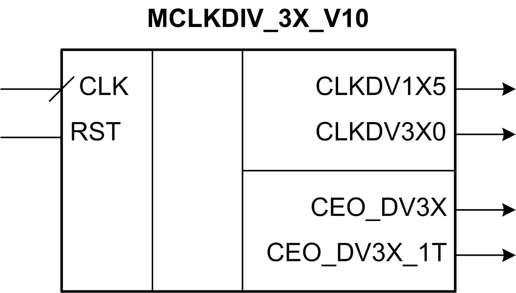
Fig. 2. Interface of a frequency divider with division factors 1.5 and 3.0
First you need to define the interface of the frequency divider. In fig. 2 shows an interface for a divider with division factors 1.5 and 3.0.
The inputs of the frequency divider are limited by two system signals for asynchronous setting of initial values RST (active high level) and a clock signal CLK, which sets the reference clock frequency. Next, we will consider the synchronization on the leading edge, in which the operation of the registers occurs when the signal at the CLK input changes from low to high.
The outputs of the divider are divided into two groups. The first group of outputs consists of signals intended for direct clocking of functional units, blocks and registers. These signals are fed to the trigger trigger inputs and have a high level duration as close as a low level duration.
The second group of signals includes CEO synchronization enable signals (Clock Enable Output), obtained on the basis of dividing the reference frequency by a natural number and having a high level duration equal to one clock cycle of the reference frequency CLK. Signals from the second group of outputs are characterized by one frequency and a fixed shift in time by a certain number of reference frequency cycles. The outputs of the CEO are focused on synchronizing functional units and blocks at a lower frequency by controlling the CE synchronization resolution circuits (Clock Enable).
Signals on the stability of the transient process are imposed on the signals of the first group, ensuring that the synchronized nodes and blocks are triggered at exactly the right time. Stability requirements were discussed in article [1].
The operation and internal organization of the frequency divider by the coefficients 1.5 and 3.0 are explained in the time diagram in fig. 3
To form the clock signals CLKDVxxx shown in the diagram is possible only with the use of a combination logic circuit. As you know, switching combinational logic can be of a multi-step character, caused by simultaneous passing of signals through various intermediate stages, which can lead to multiple switchings of the output signal during the time allotted to the response of the combinational circuit to input influences. A similar situation is unacceptable at the output of the frequency divider, because the output signal must change its state exactly two times in one period. To eliminate this effect, it is proposed to apply signals from internal registers to the combinational circuit so that simultaneous switching of two or more input signals does not occur.
The divider is based on the state machine [2], which continuously functions in the 00-01-10 cycle, which forms the signals CEO_DV3X and CEO_DV3X_1T with its states. The intermediate signal DL_STATE_1 is obtained by fixing the signal CEO_DV3X_1T with a trigger operating on the falling edge of the clock signal CLK.
A high level at the output of CLKDV1X5 is formed under the condition that the values of intermediate signals shaded in gray.
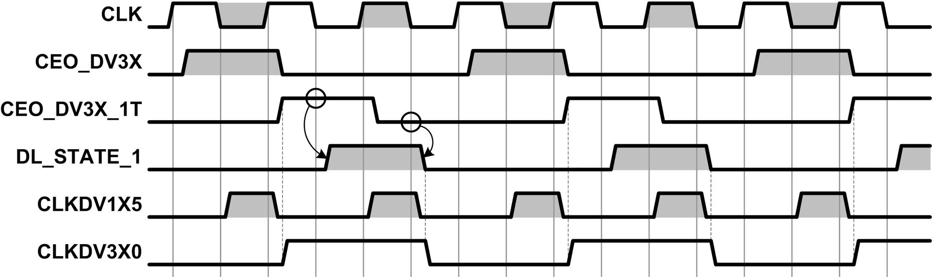
Fig. 3. Diagram of the divider with the division factors 1.5 and 3.0
The output signal CLKDV3X0 is formed by the logical addition (in positive logic) of the signals CEO_DV3X_1T (CNTR_STATE [1]) and DL_STATE_1. It is easy to see that this technical solution ensures the equality of the duration of the high and low logic levels during one period.
The following is a behavioral HDL model describing the considered frequency divider in Verilog language:
The considered frequency divider, in particular, can be used to generate clock signals of PCI buses operating at 33 and 66 MHz, using the reference frequency of 100 MHz.
The frequency divider with the coefficients of 2.0 and 4.0 is not considered in this article, since it does not apply to dividers with fractional division factors and is implemented fairly simply.

Fig. 4. Interface of a frequency divider with division factors 2.5 and 5.0
In fig. 4 presents the divider interface with coefficients 2.5 and 5.0. This divider is built according to the principles discussed above, but it is based on a more complex machine that generates internal signals and CEO signals.
The operation of the divider with coefficients 2.5 and 5.0 is explained in the diagram in fig. 5. The state machine has a four-digit internal state register and operates in a cycle 0001-0100-0010-1000-1100. The signals CEO_DV5X and CEO_DV5X_2T are derived from the low order bits of the state of the automaton. The DL_STATE_1 signal is formed by latching the signal CEO_DV5X_2T on the falling edge of the reference clock signal CLK.
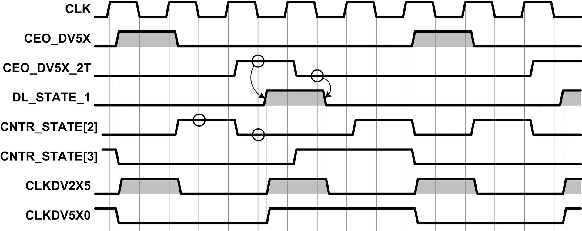
Fig. 5. Diagram of the divider with the division factors 2.5 and 5.0
The signal CLKDV2X5 is obtained by the logical addition (in positive logic) of the signals CEO_DV5X (CNTR_STATE [0]) and DL_STATE_1.
The signal CLKDV5X0 is obtained by logical addition (in positive logic) of signals CNTR_STATE [3] and DL_STATE_1.
The signals generated by the status bits of the CNTR_STATE [0] and CNTR_STATE [1] automata can be used to synchronize the functional blocks and nodes using the Clock Enable synchronization mechanism. These status bits are duplicated on the interface with the signals CEO_DV5X and CEO_DV5X_2T.
The following is a behavioral HDL model describing a frequency divider with 2.5 and 5.0 coefficients in Verilog language:
1. Borisenko N.V. Technical aspects of constructing control automata in the design of digital devices based on modern FPGA "Components and technologies" No. 12.2011.
2. Algebraic theory of automata, languages and semigroups. Edited by M. Arbib. Per. from English M., "Statistics", 1975. 335 pp .; with ill.
3. Spartan-6 Clocking Resources, www.xilinx.com/training/free-video-courses.htm#FPGA-ARC
4. Using Delay-Locked Loops in Spartan-II / IIE FPGAs, Xilinx Application Note XAPP174
When developing digital devices, it is often necessary to divide functional blocks into groups using sync signals with different parameters (the so-called synchronization domains - Clock Domain). The main parameters of any clock signal is the clock frequency and the corresponding period. Also for a number of elements, nodes and blocks, the duty cycle of the sync signal is important, which determines the duration of the low and high levels during the period, and the period instability - the “Jitter” parameter.
Despite the presence of sync signals with different parameters in the device, in most cases a single source is used to generate these signals, an external oscillator that forms the reference frequency. In specific projects, it is possible to use several generators that form non-multiple reference frequencies, for example, a 48 MHz frequency for a USB controller, a frequency of 3.6864 MHz for UART channels, and a frequency of 100 MHz for processor cores, SDRAM memory and an Ethernet network controller. The synchronization signals necessary for the normal functioning of the SBIS or FPGA functional blocks are formed from the reference signals by multiplying and dividing the frequency. The function of frequency multiplication in FPGA architecture FPGA implement nodes PLL (DLL, PLL, blocks DCM and CMT). The use of these crystal resources is described in detail by manufacturers in the relevant documentation [3,4].
Unlike frequency multipliers, frequency dividers can be built on general-purpose logical resources, based on registers and combinational circuit generators. It should be noted that the use of logical resources for the formation of a sync signal is allowed by CAD tools and the architecture of most FPGAs, but is highly discouraged by manufacturers due to the likelihood of spurious transitions and spikes in the resulting sync signal caused by switching combinational circuits. Thus, in FPGA with FPGA architecture for generating clock signals, it is preferable to use the existing infrastructure, which includes specialized crystal resources: clock input blocks, connected to specific body pins; DLL, PLL, DCM, or CMT; global synchronization networks transmitting a sync signal in the crystal volume with the least distortions.
')
There are two cases of synchronization of functional blocks and nodes at a lower frequency, obtained by dividing the reference frequency:
1. the synchronization frequency is a multiple of the reference frequency,
2. The synchronization frequency is obtained by dividing the reference frequency by a fractional coefficient.
In the first case, it is highly desirable to use the principle of synchronization resolution, which consists in the use of triggers and registers with the CE input (Clock-Enable). The organization of the elementary trigger with the CE input is shown in Fig. 1. The D-type trigger with synchronization on the front and asynchronous setting of the initial value - RST is taken as a basis. The CE input implements the principle of synchronization resolution by switching through the MX-2 multiplexer: 1 internal information input of the trigger either to an external data source - in the case of CE = “1” or output Q, with CE = “0”. The CLK clock signal is fed to the trigger input all the time, but the triggering (recording of external data) occurs exclusively in those cycles in which a log is sent to the CE input. "one".
By generating the signal CE, installed in the log. "1" during one clock cycle, and having a fixed period, which is a natural number of clock cycles, is synchronized at a lower frequency, multiple of the reference frequency.
A trigger with a CE input can be obtained from an elementary D-flip-flop by adding two transistors realizing the input multiplexer (Fig. 1). Most FPGA families contain registers with the CE input, which are technological primitives optimized at the level of the IP topology. In the absence of the need to use the synchronization enable, a permanent enable signal is supplied to the CE input.
Fig. 1. Organization of an elementary trigger with CE input
For the second case, when the sync signal is obtained by dividing the reference frequency by a fractional coefficient, using the principle of synchronization resolution is impossible due to the need to trigger downward and upward along the fronts of the reference sync signal in different clock cycles. In this case, to build a frequency divider, you will have to ignore the recommendations and use logical resources to generate the clock signal. In order to avoid races in the combinational logic it is necessary to provide input signals so that only one input signal changes its state during the response time of the output combinational circuit.
This principle of construction of the divider is relevant to use in two cases:
• absence of free frequency shaping units in FPGA FPGA architecture;
• use of the CPLD architecture of CPLD that does not have frequency shaping units.
As an example, we can consider a bunch of FPGAs of the CPLD architecture, an Atmel AVR microcontroller operating at a frequency of 16 MHz, and a reference clock signal generator with a frequency of 40 MHz. Obvious is the need to build a frequency divider by means of FPGA, which forms the microcontroller sync signal by dividing the reference frequency by a factor of 2.5.
Below are two models of frequency dividers that generate sync signals of various shapes:
• a sync signal obtained by dividing the reference frequency by a fractional coefficient;
• a sync signal obtained by dividing the reference frequency by a natural factor, but having an equal duration of high and low levels during the period;
• Signals obtained by dividing the reference frequency by the natural factor used to enable synchronization of functional blocks and nodes clocked by the reference signal.
Consider the examples of the construction of two frequency dividers with fractional division factors.
Fig. 2. Interface of a frequency divider with division factors 1.5 and 3.0
First you need to define the interface of the frequency divider. In fig. 2 shows an interface for a divider with division factors 1.5 and 3.0.
The inputs of the frequency divider are limited by two system signals for asynchronous setting of initial values RST (active high level) and a clock signal CLK, which sets the reference clock frequency. Next, we will consider the synchronization on the leading edge, in which the operation of the registers occurs when the signal at the CLK input changes from low to high.
The outputs of the divider are divided into two groups. The first group of outputs consists of signals intended for direct clocking of functional units, blocks and registers. These signals are fed to the trigger trigger inputs and have a high level duration as close as a low level duration.
The second group of signals includes CEO synchronization enable signals (Clock Enable Output), obtained on the basis of dividing the reference frequency by a natural number and having a high level duration equal to one clock cycle of the reference frequency CLK. Signals from the second group of outputs are characterized by one frequency and a fixed shift in time by a certain number of reference frequency cycles. The outputs of the CEO are focused on synchronizing functional units and blocks at a lower frequency by controlling the CE synchronization resolution circuits (Clock Enable).
Signals on the stability of the transient process are imposed on the signals of the first group, ensuring that the synchronized nodes and blocks are triggered at exactly the right time. Stability requirements were discussed in article [1].
The operation and internal organization of the frequency divider by the coefficients 1.5 and 3.0 are explained in the time diagram in fig. 3
To form the clock signals CLKDVxxx shown in the diagram is possible only with the use of a combination logic circuit. As you know, switching combinational logic can be of a multi-step character, caused by simultaneous passing of signals through various intermediate stages, which can lead to multiple switchings of the output signal during the time allotted to the response of the combinational circuit to input influences. A similar situation is unacceptable at the output of the frequency divider, because the output signal must change its state exactly two times in one period. To eliminate this effect, it is proposed to apply signals from internal registers to the combinational circuit so that simultaneous switching of two or more input signals does not occur.
The divider is based on the state machine [2], which continuously functions in the 00-01-10 cycle, which forms the signals CEO_DV3X and CEO_DV3X_1T with its states. The intermediate signal DL_STATE_1 is obtained by fixing the signal CEO_DV3X_1T with a trigger operating on the falling edge of the clock signal CLK.
A high level at the output of CLKDV1X5 is formed under the condition that the values of intermediate signals shaded in gray.
Fig. 3. Diagram of the divider with the division factors 1.5 and 3.0
The output signal CLKDV3X0 is formed by the logical addition (in positive logic) of the signals CEO_DV3X_1T (CNTR_STATE [1]) and DL_STATE_1. It is easy to see that this technical solution ensures the equality of the duration of the high and low logic levels during one period.
The following is a behavioral HDL model describing the considered frequency divider in Verilog language:
`timescale 1ns / 1ps ///////////////////////////////////////////////////////////// // Company: Argon // Engineer: FPGA-Mechanic // // Create Date: 16:27:50 03/16/2011 // Design Name: Clock Deviders // Module Name: MCLKDIV_3X_V10 // Target Devices: PLD, FPGA or ASIC // Tool versions: Xilinx ISE 10.1.03 // Description: Clock Frequency Divider by 1.5 and 3.0 // With Synchronous and Asynchronous Outputs // Revision: 1.0 // Revision 1.0 - File Created ///////////////////////////////////////////////////////////// module MCLKDIV_3X_V10( input CLK, // Sys. Clock input RST, // Asynch. Reset output CLKDV1X5, // Asynch. CL-Output Clock/1.5 // Divided Frequency (H:L=1:2) output CLKDV3X0, // Asynch. CL-Output Clock/3 // Divided Frequency (H:L=1:1) output CEO_DV3X, // Synch. FF-Output Clock Enable // Pulse (Clock/3 Frequency) output CEO_DV3X_1T // Synch. FF-Output Clock Enable // Pulse Delay 1T ); // Internal signals declaration: reg [1:0] CNTR_STATE; reg DL_STATE_1; //------------------------------------------ // Mod.3 Counter: always @ (posedge CLK, posedge RST) if(RST) CNTR_STATE <= 2'd0; else case(CNTR_STATE) 2'd0 : CNTR_STATE <= 2'd1; 2'd1 : CNTR_STATE <= 2'd2; default : // States 2 and 3: CNTR_STATE <= 2'd0; endcase //------------------------------------------ // Clock-Enable Outputs: assign CEO_DV3X = CNTR_STATE[0]; assign CEO_DV3X_1T = CNTR_STATE[1]; //------------------------------------------ // Delay for CNTR_STATE[1]: always @ (CLK, RST, CNTR_STATE[1]) if(RST) DL_STATE_1 <= 0; else if(!CLK) DL_STATE_1 <= CNTR_STATE[1]; //------------------------------------------ // Asynchronous Outputs: assign CLKDV1X5 = (~CLK & CNTR_STATE[0]) | (CLK & DL_STATE_1); assign CLKDV3X0 = CNTR_STATE[1] | DL_STATE_1; //------------------------------------------ endmodule The considered frequency divider, in particular, can be used to generate clock signals of PCI buses operating at 33 and 66 MHz, using the reference frequency of 100 MHz.
The frequency divider with the coefficients of 2.0 and 4.0 is not considered in this article, since it does not apply to dividers with fractional division factors and is implemented fairly simply.
Fig. 4. Interface of a frequency divider with division factors 2.5 and 5.0
In fig. 4 presents the divider interface with coefficients 2.5 and 5.0. This divider is built according to the principles discussed above, but it is based on a more complex machine that generates internal signals and CEO signals.
The operation of the divider with coefficients 2.5 and 5.0 is explained in the diagram in fig. 5. The state machine has a four-digit internal state register and operates in a cycle 0001-0100-0010-1000-1100. The signals CEO_DV5X and CEO_DV5X_2T are derived from the low order bits of the state of the automaton. The DL_STATE_1 signal is formed by latching the signal CEO_DV5X_2T on the falling edge of the reference clock signal CLK.
Fig. 5. Diagram of the divider with the division factors 2.5 and 5.0
The signal CLKDV2X5 is obtained by the logical addition (in positive logic) of the signals CEO_DV5X (CNTR_STATE [0]) and DL_STATE_1.
The signal CLKDV5X0 is obtained by logical addition (in positive logic) of signals CNTR_STATE [3] and DL_STATE_1.
The signals generated by the status bits of the CNTR_STATE [0] and CNTR_STATE [1] automata can be used to synchronize the functional blocks and nodes using the Clock Enable synchronization mechanism. These status bits are duplicated on the interface with the signals CEO_DV5X and CEO_DV5X_2T.
The following is a behavioral HDL model describing a frequency divider with 2.5 and 5.0 coefficients in Verilog language:
`timescale 1ns / 1ps ///////////////////////////////////////////////////////////// // Company: Argon // Engineer: FPGA-Mechanic // // Create Date: 16:27:50 03/16/2011 // Design Name: Clock Deviders // Module Name: MCLKDIV_5X_V10 // Target Devices: PLD, FPGA or ASIC // Tool versions: Xilinx ISE 10.1.03 // Description: Clock Frequency Divider by 2.5 and 5.0 // With Synchronous and Asynchronous Outputs // Revision: 1.0 // Revision 1.0 - File Created ///////////////////////////////////////////////////////////// module MCLKDIV_5X_V10( input CLK, // Sys. Clock input RST, // Asynch. Reset output CLKDV2X5, // Asynch. CL-Output Clock/2.5 // Divided Frequency (H:L=2:5) output CLKDV5X0, // Asynch. CL-Output Clock/5 // Divided Frequency (H:L=1:1) output CEO_DV5X, // Synch. FF-Output Clock Enable // Pulse (Clock/5 Frequency) output CEO_DV5X_2T // Synch. FF-Output Clock Enable // Pulse Delay 2T ); // Internal signals declaration: reg [3:0] CNTR_STATE; reg DL_STATE_1; //------------------------------------------ // Mod.5 Counter: always @ (posedge CLK, posedge RST) if(RST) CNTR_STATE <= 4'd1; else case(CNTR_STATE) 4'd1 : CNTR_STATE <= 4'd4; 4'd4 : CNTR_STATE <= 4'd2; 4'd2 : CNTR_STATE <= 4'd8; 4'd8 : CNTR_STATE <= 4'd12; 4'd12 : CNTR_STATE <= 4'd1; default : // Other States : CNTR_STATE <= 4'd1; endcase //------------------------------------------ // Clock-Enable Outputs: assign CEO_DV5X = CNTR_STATE[0]; assign CEO_DV5X_2T = CNTR_STATE[1]; //------------------------------------------ // Delay for CNTR_STATE[1]: always @ (CLK, RST, CNTR_STATE[1]) if(RST) DL_STATE_1 <= 0; else if(!CLK) DL_STATE_1 <= CNTR_STATE[1]; //------------------------------------------ // Asynchronous Outputs: assign CLKDV2X5 = CNTR_STATE[0] | DL_STATE_1; assign CLKDV5X0 = CNTR_STATE[3] | DL_STATE_1; //------------------------------------------ endmodule Quoted literature
1. Borisenko N.V. Technical aspects of constructing control automata in the design of digital devices based on modern FPGA "Components and technologies" No. 12.2011.
2. Algebraic theory of automata, languages and semigroups. Edited by M. Arbib. Per. from English M., "Statistics", 1975. 335 pp .; with ill.
3. Spartan-6 Clocking Resources, www.xilinx.com/training/free-video-courses.htm#FPGA-ARC
4. Using Delay-Locked Loops in Spartan-II / IIE FPGAs, Xilinx Application Note XAPP174
Source: https://habr.com/ru/post/306132/
All Articles