How Linkmeup went to visit “STC Metrotek”
For almost a week, as Peter was without a window, the entire local population finally switched to gill breathing and laughed at the guests of the city, as well as those who have not yet developed the much needed skill here. The situation required decisive action and Linkmeup editors made a strategic decision to visit. The choice fell on the "STC Metrotek" , they called to themselves for a long time and promised an interesting pastime. According to the results of the visit, this report was written, which is offered to your attention.
Attention! Under the cut text with pictures. The quality of the pictures can greatly upset creative individuals, but we only had a long-focus lens. Our business is to warn.
')
“Scientific and Technical Center Metrotek” - since 2003, has been developing devices for carrying out measurements on communication networks, analyzers and switches, providing a full development cycle from board design to software stuffing at all levels. They have deserved reasons for pride: the first compact analyzer Gigabit ethernet, and then 10G was created in Russia, and then the 100G analyzer-balancer came out altogether. They know about networks almost everything. Owners of OUI numbers, which in itself inspires. Read RFC 2544 and its Y.1564 recommendation. Presented on the international market. They actively participate in specialized events dedicated to microcontrollers, Linux, etc., work with students, conduct training courses on programming, and take internships.
STC Metrotek is located in the business center near the metro station Pionerskaya, where you can easily walk for 10 minutes at a leisurely pace. Even before going on a visit, it was known that at the designated address everything was at once - both development and production. But on arrival at the site, it turned out that Metrotek STC is located on an unexpectedly modest area for its scale.
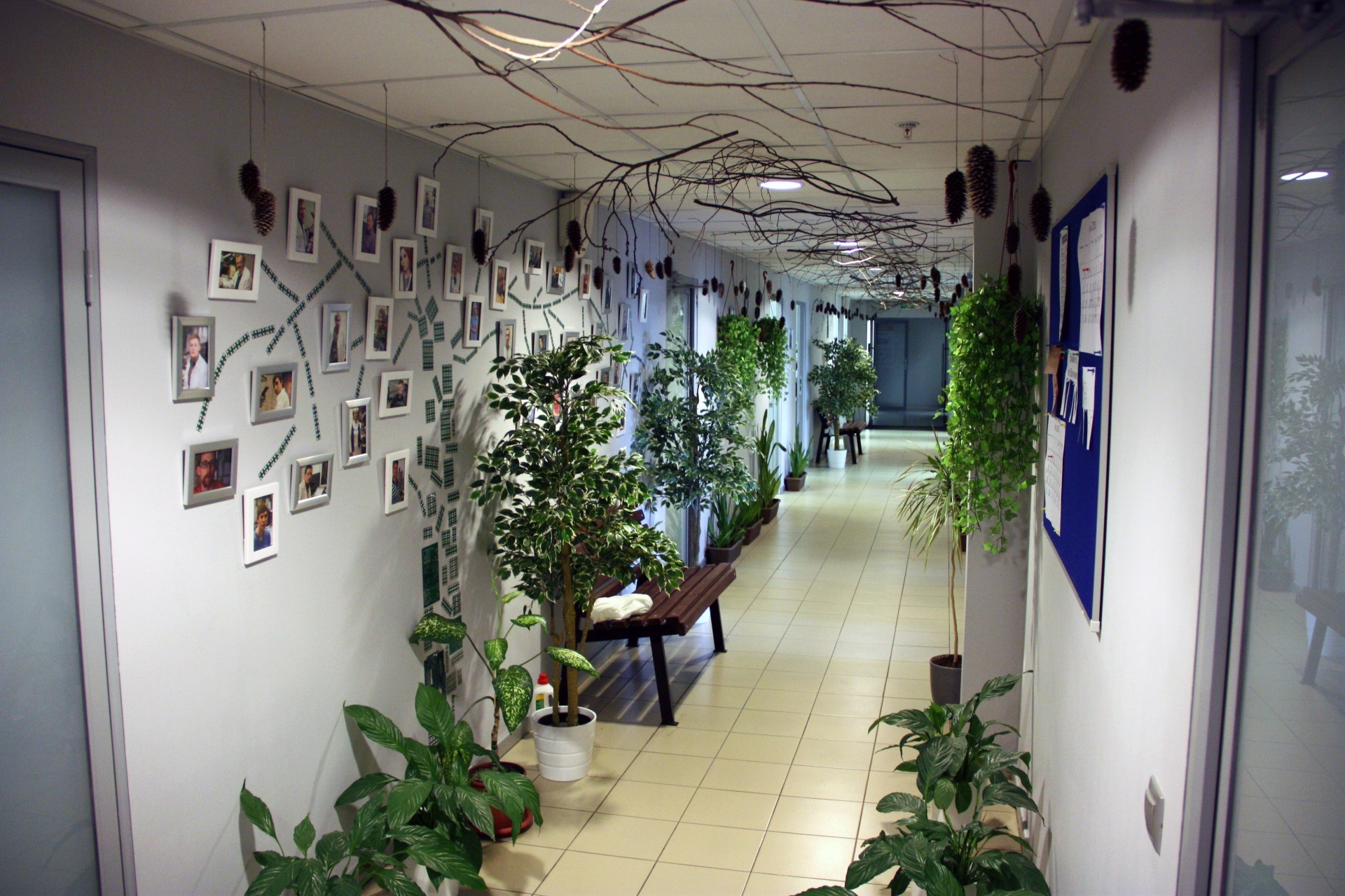
Main office corridor
The beautiful Natalia, who met us, first of all took us to Pechenkovaya (it was written on the door), gave us coffee and buns, announced a pizza at the end of the tour and clarified the discrepancy in seeing the huge production areas and the actual size of the office. It turns out that the postscript at the beginning of the name - STC is there not just for beauty or solidity, but reflects the main task of the company - to conduct research and exploration work, including, to engage in small-scale production of devices. Small series, in this case, means a batch of up to 1000 pieces. In the case of large orders, or when performing technically complex installation, STC Metrotek has local partners. By the way, usually, the entire production cycle is closed within St. Petersburg. Perhaps that is why the design of their devices used the whole palette of gray =)
Our guide Natalia and Julia Valerievna meeting everyone
We arrived on the verge of a foul, that is, at the moment when the working day of most of the employees was already over, but we still had chances to catch the most persistent and experienced. Right from the threshold, they noted that there is a presence of power in the office and some kind of the right atmosphere of a place where it is pleasant to be and work. A little later, it came to the realization that this is all due to the attention to detail and the desire of local girls to embellish this scientific and technical paradise. Although on closer examination it turned out that half of the green plantings in the office are brazenly plastic, but we were assured that this attack would soon be defeated, but all the cones hanging in the corridor are strictly natural and collected personally in the nearby forest.
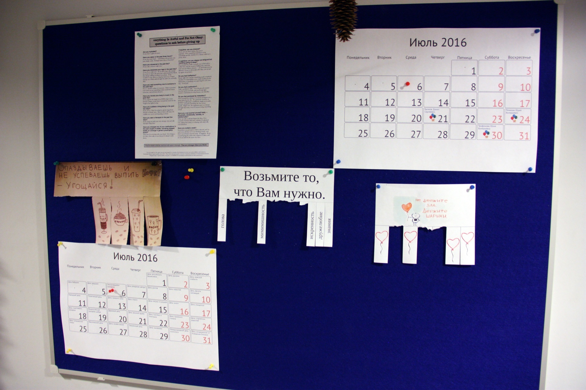
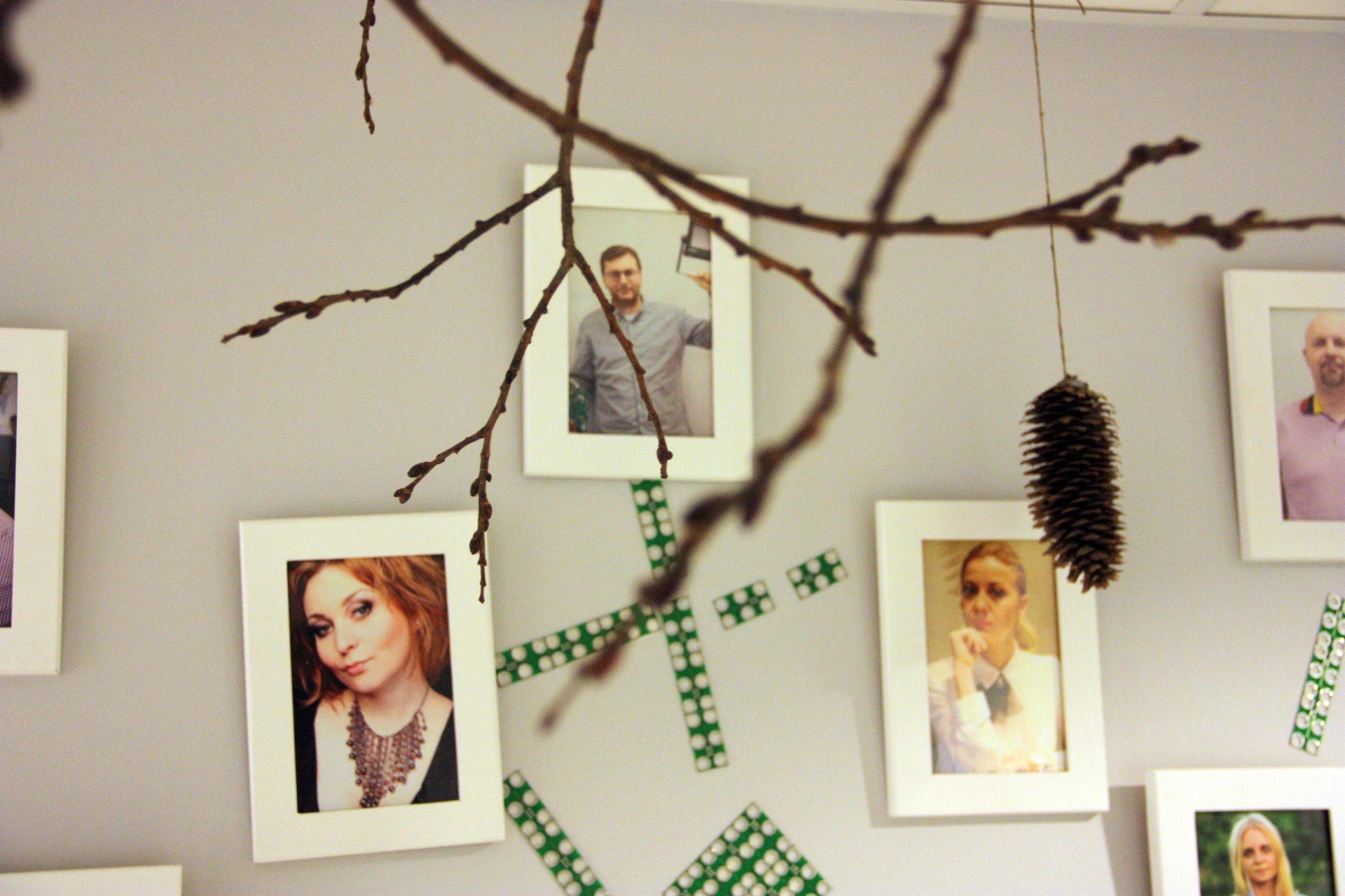
Those nice details
Immediately after the reception there are three sacral things - an office bulletin board, a textolite stylized tree with photos of employees and, suddenly, a server room. There were no admins anymore, and they are not allowed to go there without them, but Natalia assured us that there is just a server and nothing surprising. They did not argue, but they noted to themselves that everything in the office is connected via 10G optics. What for? Well, obviously, the office lives on diskless machines, working on Linux terminals. The review author strongly endorses such decisions.
We decided to make our walk around the office along the technological chain of developing any local device, since here it is different from the usual soft and better give a brief explanation.
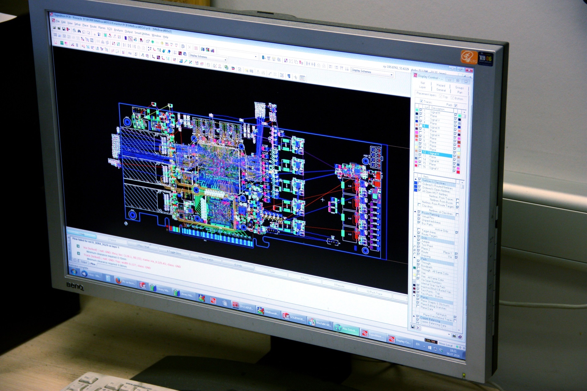
Feeling weak to color and incomprehensible pictures
It all starts with an idea. But here the idea cannot exist by itself and soar detached from the realities of the world. The idea should be immediately wrapped up in the technical capabilities of modern microelectronics, in parallel finding the pitfalls, considering methods of solving and opening up interesting possibilities. The first to translate ideas come from circuitry. They develop a circuit board, which is produced in production. Then, still a warm board, falls into the hands of engineers, designers, who bring to mind the technical and logical stuffing, teaching the board to interact with the operating system. But the farther into the forest, the more code and at the next stage, FPGA programmers take on the task. From the task to teach a new device to use all its power for the benefit of civilization, implementing logic circuits. And last in turn, but not least, application development, which implements the necessary tests programmatically and makes the user interface, takes on the case.
And now we go to each department for a more detailed acquaintance.
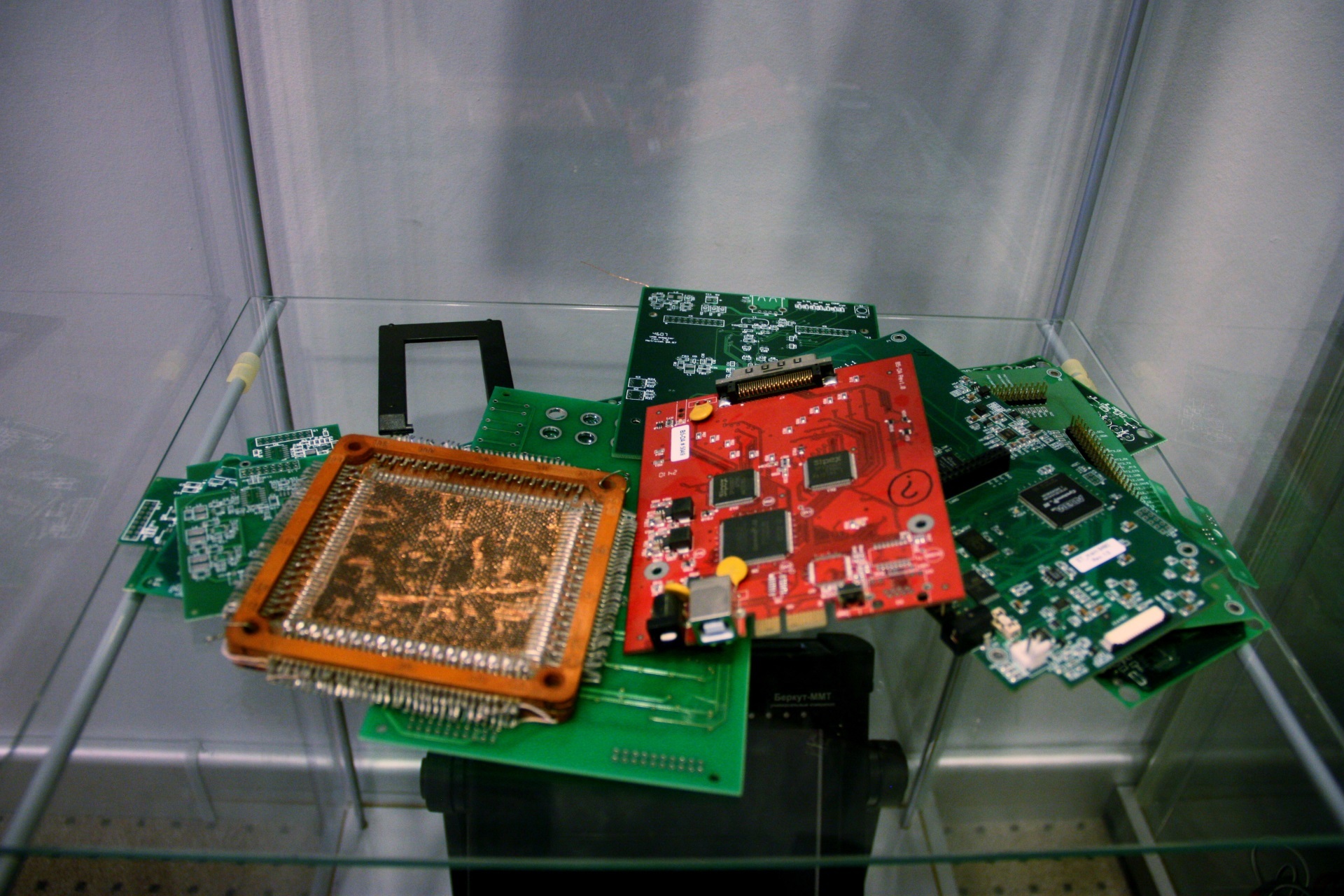
Slice Hall of Fame
So, there is an idea, a theory has been worked out, which means it’s time to start practicing. The first who takes a hit, this circuitry. Applying the magic of software for tracing, they make the design of future boards. Some averaged device here is made on a six-layer PCB, but sometimes it comes to serious development on 22 layers. For example, in the current main pride of the STC Metrotek - Berkut B100 switch, such cards are used. Actually, here it is:
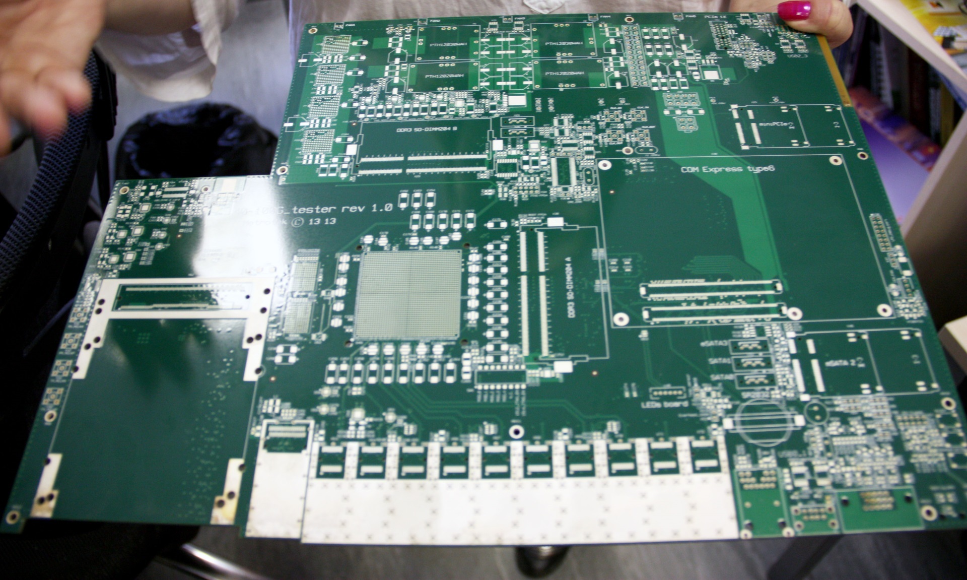
Fee from B100, in which the mother gave birth
A closer look reveals that the board has the structure of a classical general-purpose motherboard - a place for a processor (specifically, Corei7), So-Dimm memory, PCI-e bus, eSATA, etc. That's just an ordinary Nurse is 4, at least 6 layers, and here more than twenty. You look at this disgrace and you want to convey ardent greetings to all who buried the domestic microelectronics.
Well, not really wanted
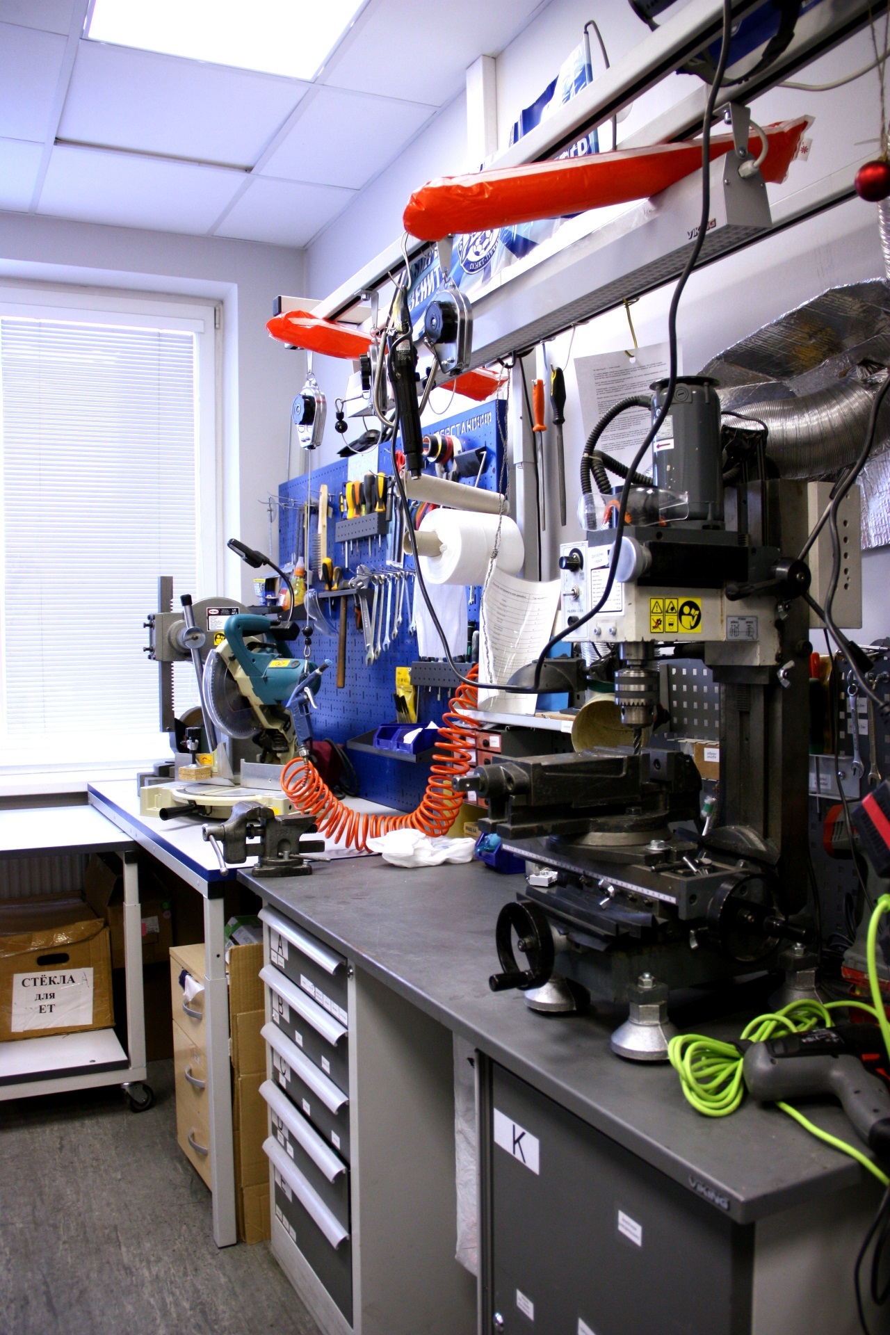
Again leads thought to the side. At this time I want to say a little about jobs. And this is the purest functionality without the frills. I want to clap my palms with delight. Absolutely all the offices are of the same size (even for high authorities), each has 3-4 people, depending on the type of activity and the need for placing stands. Ergonomic chairs, no one bothers anyone and no godless openspaces. Sit and work for your pleasure. By the way, one of the development teams is led directly by the director of the STC Metrotek, for the director is good, but they remember their hands.
Perhaps this is the most responsible circuit design Metroteka
According to the mind, after the circuit engineers should be a story about the production, but by itself there will be a lot of pictures, so it is better to leave them for sweet, but for now let's talk about the development. After the finished board comes out of production, three operations need to be done with it: write drivers and prepare the system core. And at the same time to carry out optimization.
Shift a couple of doors and find ourselves in a group of design engineers. They are engaged in the achievement of the common good: they build in Wi-Fi modules, launch non-standard software on testers, optimize work with batteries, etc.
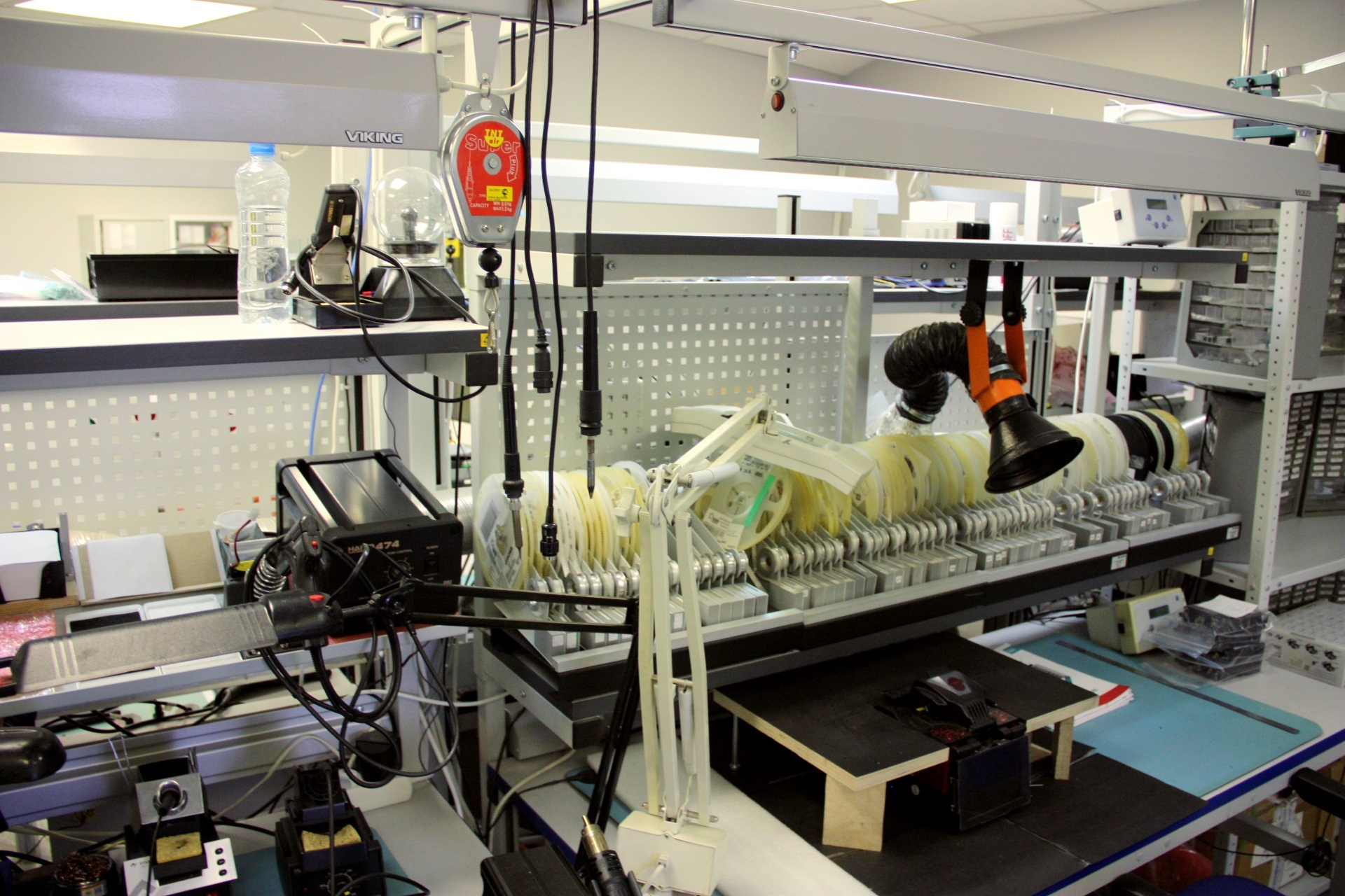
Having received a strict order not to go anywhere hands for everything is included and under voltage, we boldly go inside. Their office was the most vivid impression at that time. Due to the fact that system development is neatly between the hardware and the software, these guys equally cheerfully know how to solder and write code.
Typical workplace
In the office under the dimensional crack of the oscilloscope and the smell of rosin, there is a mystery of writing drivers, soldering additional modules, OS kernel configuration and tracking package dependencies. Sometimes this leads to the creation of funny monsters, but this does not make them less attractive. And by itself, Qt is loved here.
Strictly speaking, the system development team ensures a calm and carefree operation of the device management software interfaces for which the application team is responsible. But let's not get ahead.
As is a creative mess
Having said goodbye to the designers, we boldly open the door to the FPGA developers and find them after completing another feature to all the same B100.
B100 is clearly pleased with the new feature and does not hide it.
Here I want to explain why all the same FPGA? Why are they so wonderful?
Once we have already devoted a whole issue to this topic , but for those who missed, we offer a brief semantic squeeze.
So, the first and most important thing is FPGA, in contrast to other PLDs (they are also FPGAs), which allows the user to configure their functional part in almost any way, often limited only by imagination. If you want a powerful number of chips, implement a thousand multipliers, if you want a network controller, please see how the new-fashioned HMC memory works - flag in hand. In reality, this means that even after the release of the device, the developer leaves himself the opportunity to fix iron bugs. There are a million and a thousand examples when a batch of network cards sold on ASIC was released, where later there was a minor but very unpleasant bug that could not be fixed at the driver level and the manufacturer, blushing, released a new revision of devices, causing serious losses. And do not forget to keep in mind that the timing of the release of a new revision is calculated for months at best. In the case of FPGA, the average error correction takes two weeks. Or faster, if the joint came out quite unpleasant.
The second plus, and many consider it more important than the first, is the capacity for giant parallelism. For example, on one modest chip there are 48 transceivers, each of which provides a transmission and reception speed of 12 Gbit / s. Multiply the first to the second and get> 500 Gbit / s. Very impressive figure. And here the FPGA developer enters the battle. It depends only on him how to pacify such power, intelligently dissolve the flow of information and ensure the greatest performance, coupled with stability.
Satisfied developer talks about his brainchild
Now Metrotek actively working with a relatively new platform - SoC (System on Chip). The meaning of SoC is the placement of the functionality of a complete system in one chip. For example, you can combine ARM, FPGA and a piece of memory under the same roof. This will give a tremendous speed of internal communication within a single crystal, freeing from bottlenecks in the form of various data transfer buses. The speed depends on the crystal, but data processing at a speed of 560 Gbit / s is quite real numbers.
They say that if you look for a long time, it will not become clearer
Exiting delightfully, we are heading towards the final stage - towards applied development.
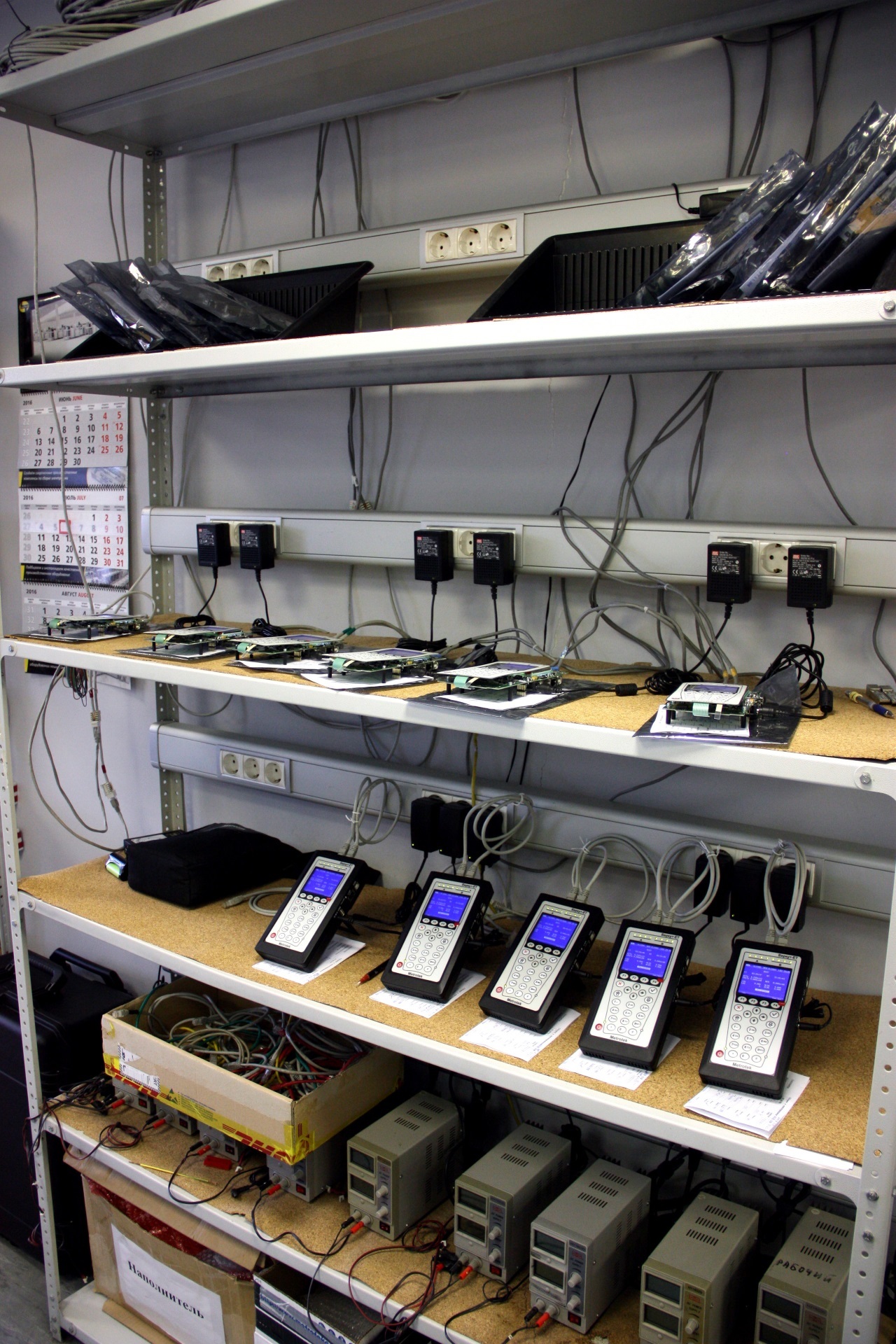
This is the realm of Android, user menus and measurement interfaces. Everything written is tested here, on live equipment. The software is developed on the Apache Cordova platform, which interacts with the system through a previously written API using the USB / IP interface. The creators of the API are sitting at the next door, so that all issues are resolved very quickly.
Maybe I'm already tired, but once again I remind you that the set of tests implemented by the instruments and their algorithms are not taken from the ceiling, but strictly from the RFC and additions to them.
Test bench option
At the beginning of the article it was stated that the STC Metrotek does not occupy super large areas, but has its own production. The output power is at the level of provision of working samples of the designed devices and provision of small-scale assembly. But sometimes additional factors come into play — for example, the B100 board, just physically does not fit in the local soldering furnace, and buying a larger amount for the sake of single orders is meaningless.
Without a general view can not
Contrary to the established traditions, only men work on the installation here. This is probably a consequence of the very small-scale, when the tasks are not worth a day to sit on the conveyor and poke a soldering iron in the same place, the same parts.
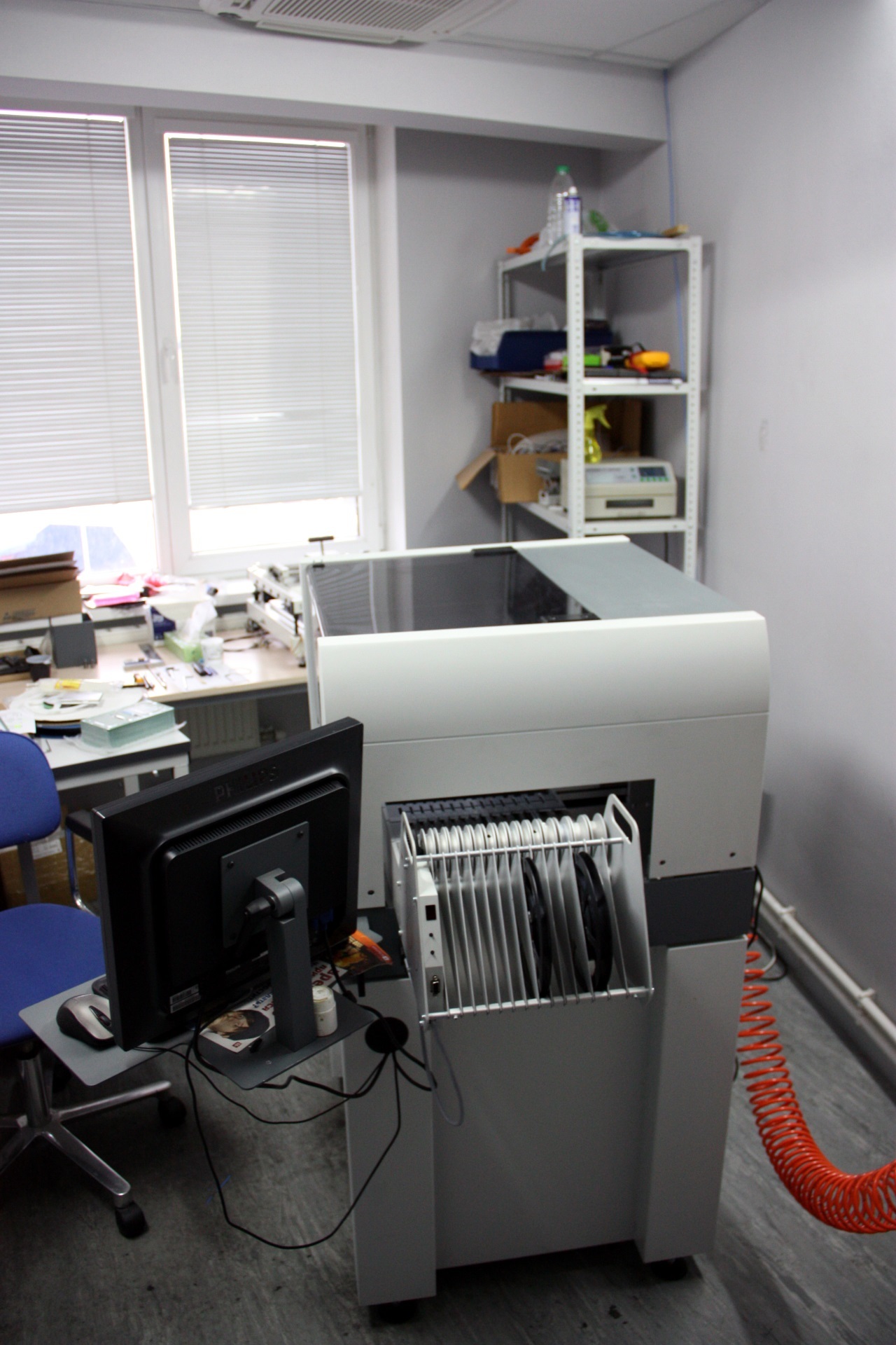
Of course, it’s not by one manual assembly that the workshop is alive and they have a machine for mounting a small scatter. He stands in a separate clean room, quite happy with everything, although it does not hit performance. We found him in an uncharged state, sighed sadly and returned to the assembly hall.
Here it is, Chinese laborer
Conducting a further inspection of the premises, it was noted that in addition to the classic installation of parts on the board, the optical part of the OTDR was also being cooked to complete the OTDR testers with modules. Also, from the interesting, a workshop was created to create plastic cases, models of new devices or just to finish them in place. As popular wisdom says - after assembly, carefully process the file. Or even a circular.
When you see a circular, and behind the wall is mounting 0.1-0.2 elements
But we move further along the technological chain. After the device is assembled and the firmware is poured into it, everyone without exception is sent to a simple daily test - looped and included in the measurement test. If the day the fighter lasted and did not go smoke, it means fit for military service. According to statistics, a day is enough to identify all the problematic elements.
Testing testers at various stages of assembly
Each device has a passport, which starts simultaneously with the installation, which indicates its entire history, including who installed which items, who tested, calibrated, what firmware was installed, and so on. Keeping such strict reporting allows certification of devices for using their testimony as evidence in court. Now, your provider will answer for the braking tanchiki to the fullest extent!
It should be noted that all equipment is made as suitable as possible for the harsh conditions of field operation. For example, the MMT Eagle, which is a modular configurable platform, could be two times smaller, but for the sake of durability it was necessary to sacrifice miniature and pack it in a strong iron case. But the devices are certified according to the strength class and can be safely dropped to the floor several times a day.
Patient Golden Eagle MMT
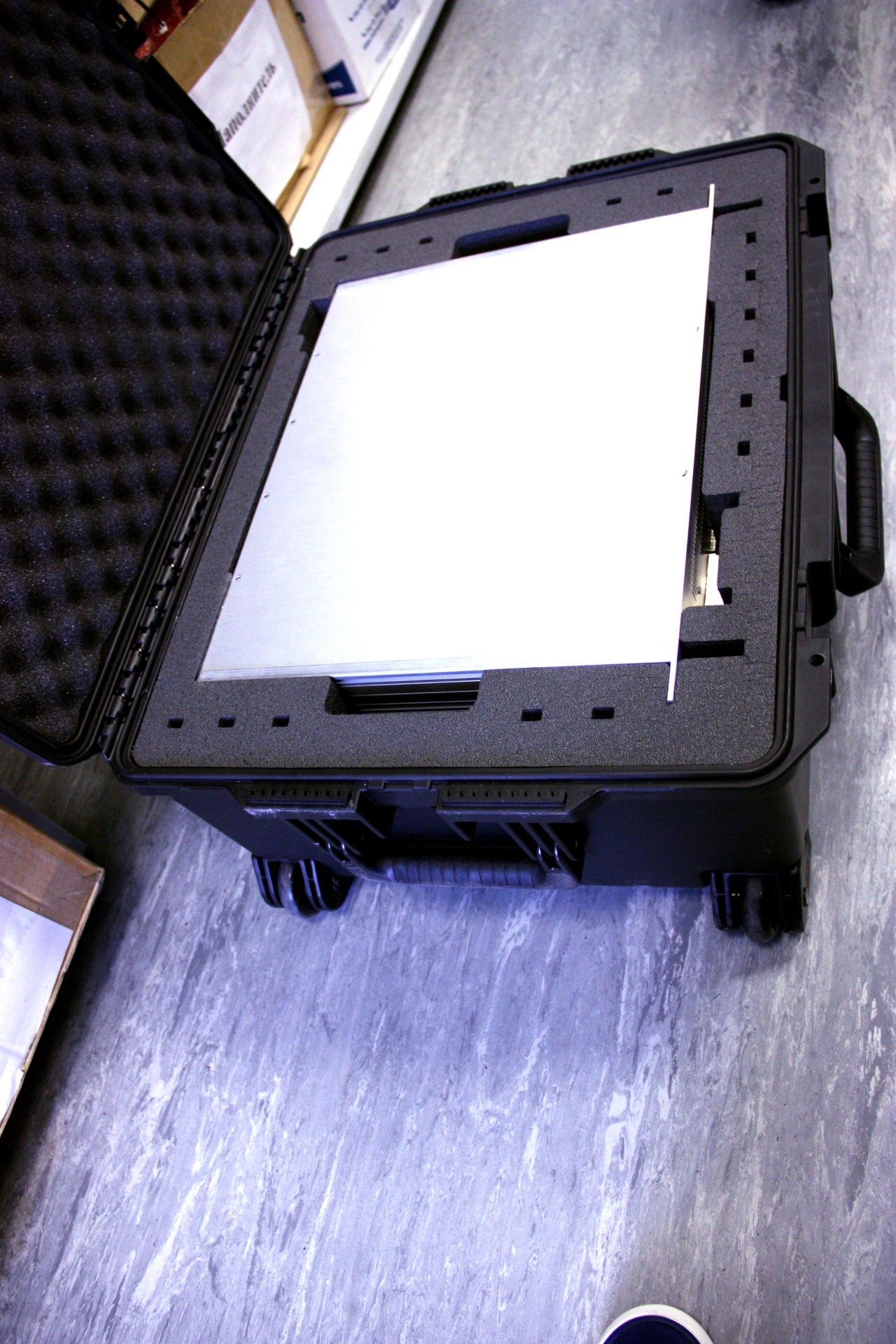
After the tests, the instruments are packed and shipped to the customer. And here we are naturally surprised. The concept of good packaging has reached a new level. The most valuable equipment of STC Metrotek delivers exclusively in shock-resistant cases, without any exceptions. They can be safely thrown out of the window or planted on top of a young elephant. The electronics inside will remain intact, in its foam rubber kingdom.
Practice has shown that it is better to supply good equipment with a good suitcase. It is cheaper for itself, and customers who are accustomed to cardboard packaging feel a sense of genuine delight. Rumor has it that the most agile guys use these bags for travel. It is unlikely that your socks and T-shirts will feel more comfortable than in this suitcase.
B100 surrounded by care and gentleness
Finally, looked at the local museum, which collected samples of all previously produced devices. Of the interesting was noted BERcut-MMT, the first generation, the design of which from and to, was made solely by the developers.
Design from engineers. He exists.
A demo stand, which is in the process of reassembly, was not far behind, so it wasn’t enough to boast. Well, at least the top LEDs included.
The entire Linkmeup edition loves telling success stories of telecommunication companies that have emerged in the post-Soviet space.
“STC Metrotek” can be safely called a pearl and set an example for everyone. This company conducts its business, not starting from the western giants of the industry, but actively competes with them and constantly produces advanced devices that meet the changing realities of modern times.
For example, their very first device, the Berkut-S, the compact E1 analyzer, based on the iPAQ, frankly surpassed its time. Then any analyzer had to get into a large backpack with difficulty, and at least two had to maintain it. Operators did not believe, took tests, were delighted and were afraid to give it to field engineers because or lose or steal. And then the iPAQ, as a platform, died at all, but the engineers of STC Metrotek did not give up, but continued to work hard, continuing to please all signalers with their devices.
Therefore, I sincerely want to wish the children further development, strengthen their presence in international markets and please us with a device that will first provide a new standard of testing not only in the CIS, but throughout the world as a minimum.
And while we go eat a cooling pizza and write this report.
Attention! Under the cut text with pictures. The quality of the pictures can greatly upset creative individuals, but we only had a long-focus lens. Our business is to warn.
')
History reference
“Scientific and Technical Center Metrotek” - since 2003, has been developing devices for carrying out measurements on communication networks, analyzers and switches, providing a full development cycle from board design to software stuffing at all levels. They have deserved reasons for pride: the first compact analyzer Gigabit ethernet, and then 10G was created in Russia, and then the 100G analyzer-balancer came out altogether. They know about networks almost everything. Owners of OUI numbers, which in itself inspires. Read RFC 2544 and its Y.1564 recommendation. Presented on the international market. They actively participate in specialized events dedicated to microcontrollers, Linux, etc., work with students, conduct training courses on programming, and take internships.
Dislocation
STC Metrotek is located in the business center near the metro station Pionerskaya, where you can easily walk for 10 minutes at a leisurely pace. Even before going on a visit, it was known that at the designated address everything was at once - both development and production. But on arrival at the site, it turned out that Metrotek STC is located on an unexpectedly modest area for its scale.
Main office corridor
The beautiful Natalia, who met us, first of all took us to Pechenkovaya (it was written on the door), gave us coffee and buns, announced a pizza at the end of the tour and clarified the discrepancy in seeing the huge production areas and the actual size of the office. It turns out that the postscript at the beginning of the name - STC is there not just for beauty or solidity, but reflects the main task of the company - to conduct research and exploration work, including, to engage in small-scale production of devices. Small series, in this case, means a batch of up to 1000 pieces. In the case of large orders, or when performing technically complex installation, STC Metrotek has local partners. By the way, usually, the entire production cycle is closed within St. Petersburg. Perhaps that is why the design of their devices used the whole palette of gray =)
Our guide Natalia and Julia Valerievna meeting everyone
Let's hit the road
We arrived on the verge of a foul, that is, at the moment when the working day of most of the employees was already over, but we still had chances to catch the most persistent and experienced. Right from the threshold, they noted that there is a presence of power in the office and some kind of the right atmosphere of a place where it is pleasant to be and work. A little later, it came to the realization that this is all due to the attention to detail and the desire of local girls to embellish this scientific and technical paradise. Although on closer examination it turned out that half of the green plantings in the office are brazenly plastic, but we were assured that this attack would soon be defeated, but all the cones hanging in the corridor are strictly natural and collected personally in the nearby forest.
Those nice details
Immediately after the reception there are three sacral things - an office bulletin board, a textolite stylized tree with photos of employees and, suddenly, a server room. There were no admins anymore, and they are not allowed to go there without them, but Natalia assured us that there is just a server and nothing surprising. They did not argue, but they noted to themselves that everything in the office is connected via 10G optics. What for? Well, obviously, the office lives on diskless machines, working on Linux terminals. The review author strongly endorses such decisions.
How it works
We decided to make our walk around the office along the technological chain of developing any local device, since here it is different from the usual soft and better give a brief explanation.
Feeling weak to color and incomprehensible pictures
It all starts with an idea. But here the idea cannot exist by itself and soar detached from the realities of the world. The idea should be immediately wrapped up in the technical capabilities of modern microelectronics, in parallel finding the pitfalls, considering methods of solving and opening up interesting possibilities. The first to translate ideas come from circuitry. They develop a circuit board, which is produced in production. Then, still a warm board, falls into the hands of engineers, designers, who bring to mind the technical and logical stuffing, teaching the board to interact with the operating system. But the farther into the forest, the more code and at the next stage, FPGA programmers take on the task. From the task to teach a new device to use all its power for the benefit of civilization, implementing logic circuits. And last in turn, but not least, application development, which implements the necessary tests programmatically and makes the user interface, takes on the case.
And now we go to each department for a more detailed acquaintance.
Slice Hall of Fame
Circuitry
So, there is an idea, a theory has been worked out, which means it’s time to start practicing. The first who takes a hit, this circuitry. Applying the magic of software for tracing, they make the design of future boards. Some averaged device here is made on a six-layer PCB, but sometimes it comes to serious development on 22 layers. For example, in the current main pride of the STC Metrotek - Berkut B100 switch, such cards are used. Actually, here it is:
Fee from B100, in which the mother gave birth
A closer look reveals that the board has the structure of a classical general-purpose motherboard - a place for a processor (specifically, Corei7), So-Dimm memory, PCI-e bus, eSATA, etc. That's just an ordinary Nurse is 4, at least 6 layers, and here more than twenty. You look at this disgrace and you want to convey ardent greetings to all who buried the domestic microelectronics.
Well, not really wanted
Again leads thought to the side. At this time I want to say a little about jobs. And this is the purest functionality without the frills. I want to clap my palms with delight. Absolutely all the offices are of the same size (even for high authorities), each has 3-4 people, depending on the type of activity and the need for placing stands. Ergonomic chairs, no one bothers anyone and no godless openspaces. Sit and work for your pleasure. By the way, one of the development teams is led directly by the director of the STC Metrotek, for the director is good, but they remember their hands.
Perhaps this is the most responsible circuit design Metroteka
Development in three steps
According to the mind, after the circuit engineers should be a story about the production, but by itself there will be a lot of pictures, so it is better to leave them for sweet, but for now let's talk about the development. After the finished board comes out of production, three operations need to be done with it: write drivers and prepare the system core. And at the same time to carry out optimization.
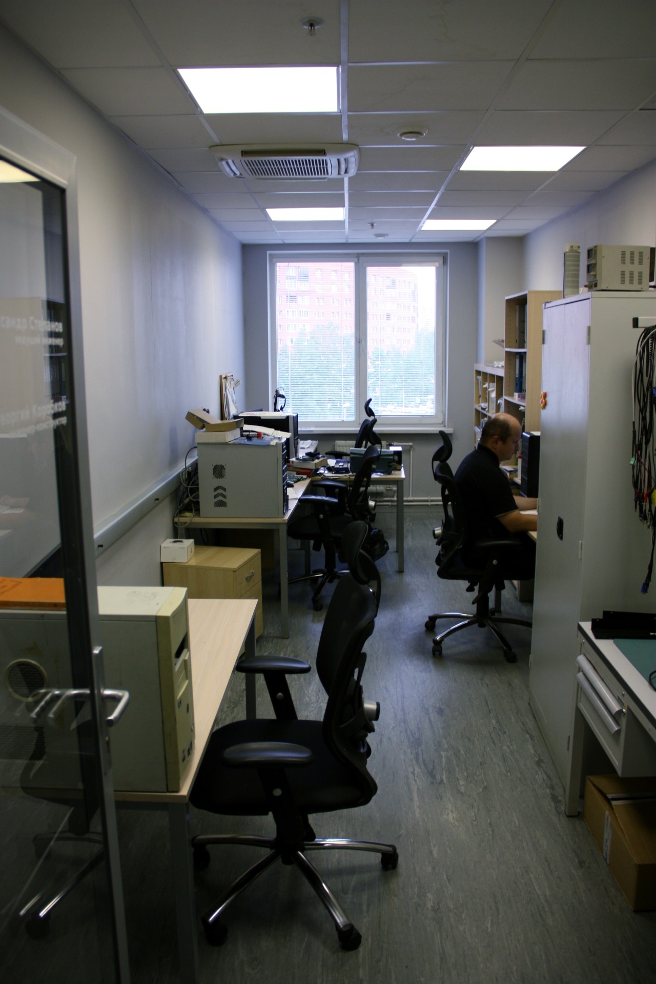
Shift a couple of doors and find ourselves in a group of design engineers. They are engaged in the achievement of the common good: they build in Wi-Fi modules, launch non-standard software on testers, optimize work with batteries, etc.
Having received a strict order not to go anywhere hands for everything is included and under voltage, we boldly go inside. Their office was the most vivid impression at that time. Due to the fact that system development is neatly between the hardware and the software, these guys equally cheerfully know how to solder and write code.
Typical workplace
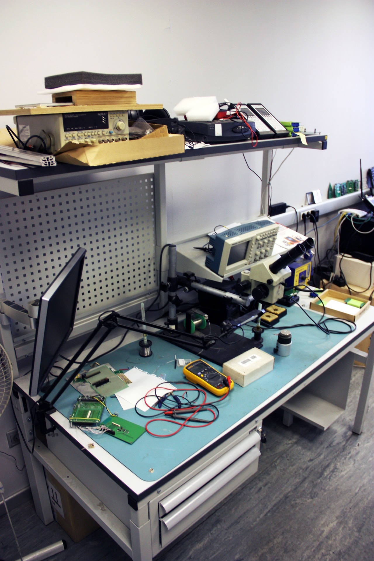
In the office under the dimensional crack of the oscilloscope and the smell of rosin, there is a mystery of writing drivers, soldering additional modules, OS kernel configuration and tracking package dependencies. Sometimes this leads to the creation of funny monsters, but this does not make them less attractive. And by itself, Qt is loved here.
Strictly speaking, the system development team ensures a calm and carefree operation of the device management software interfaces for which the application team is responsible. But let's not get ahead.
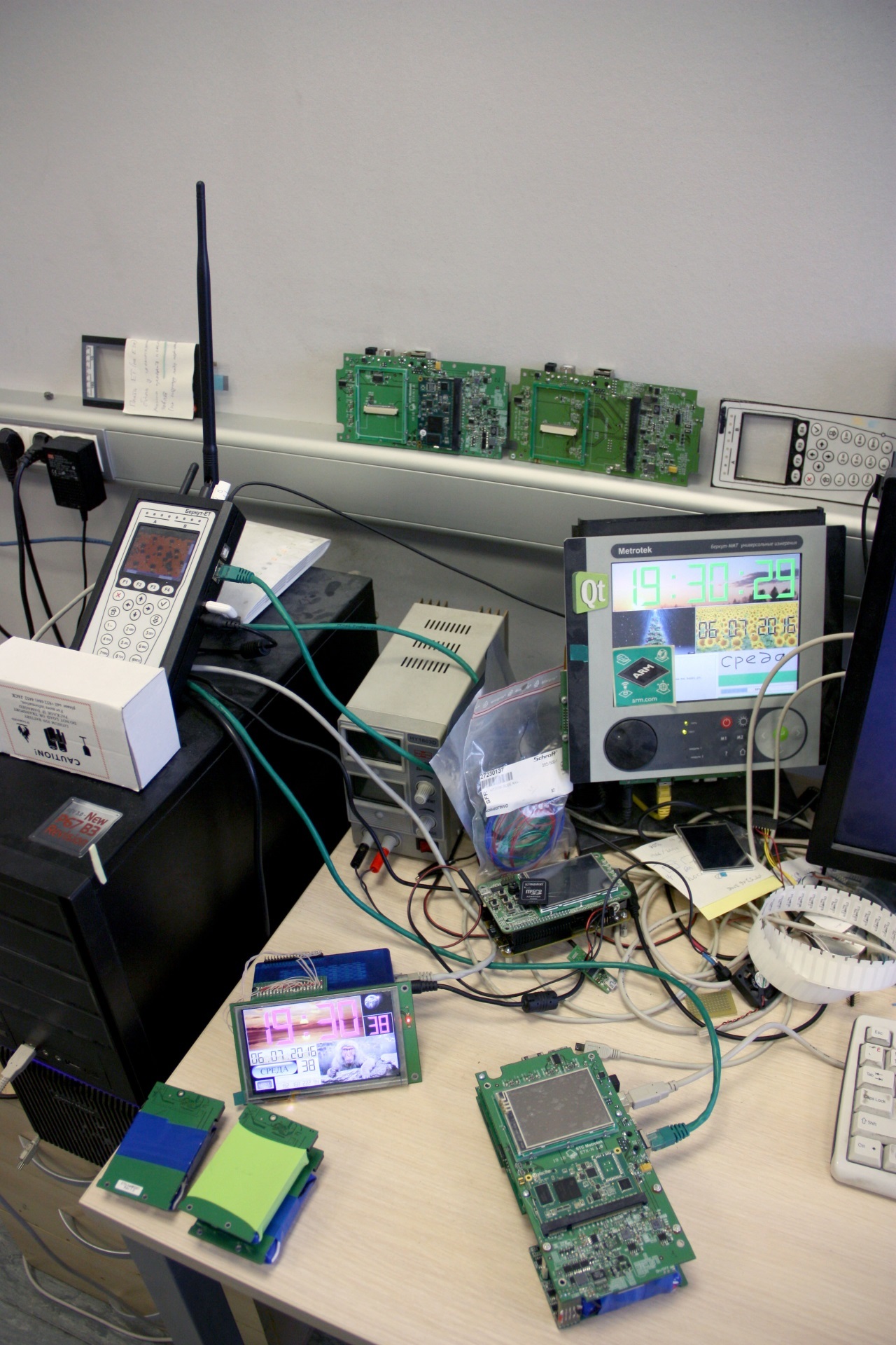
As is a creative mess
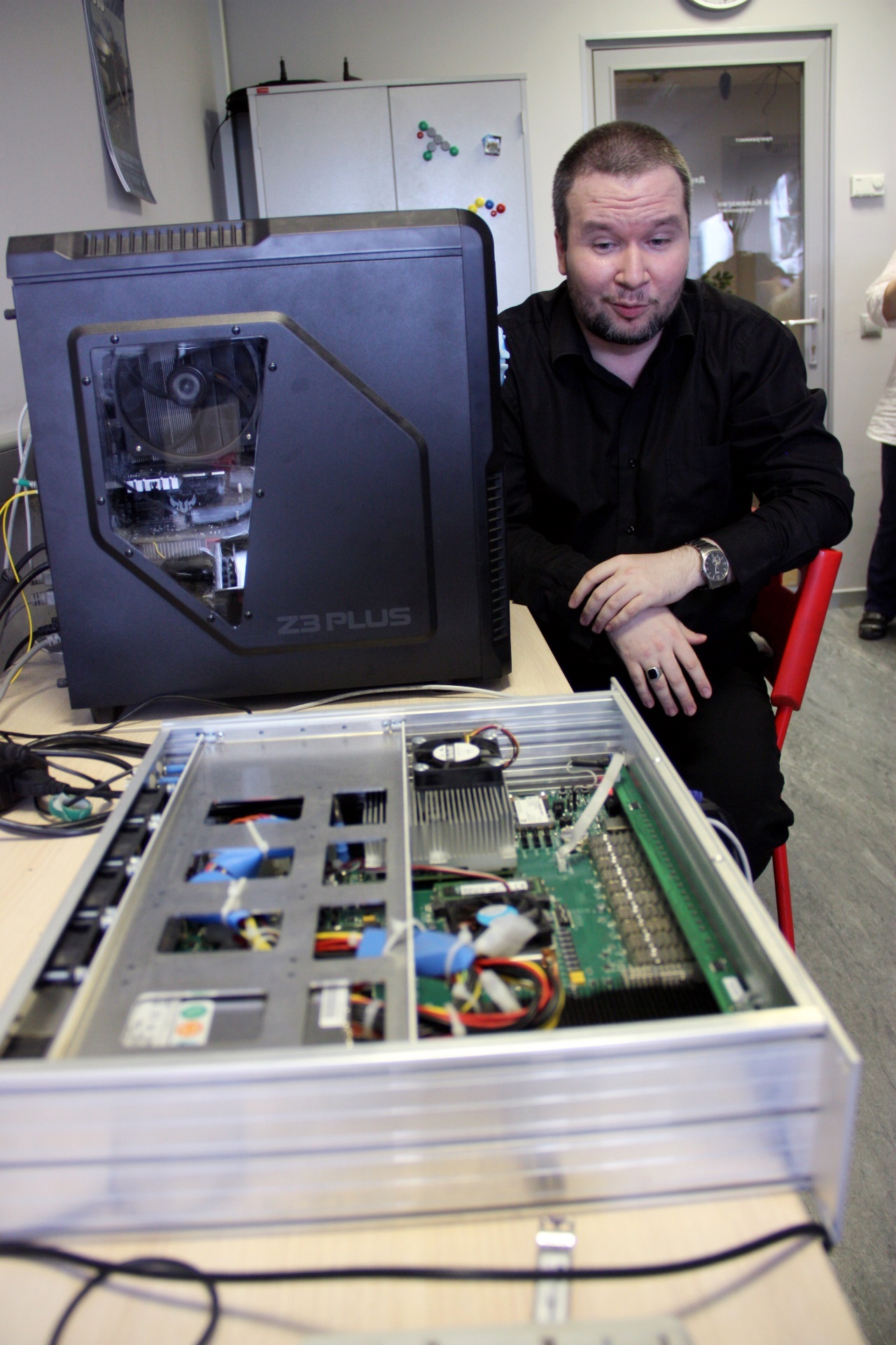
Having said goodbye to the designers, we boldly open the door to the FPGA developers and find them after completing another feature to all the same B100.
B100 is clearly pleased with the new feature and does not hide it.
Here I want to explain why all the same FPGA? Why are they so wonderful?
Once we have already devoted a whole issue to this topic , but for those who missed, we offer a brief semantic squeeze.
So, the first and most important thing is FPGA, in contrast to other PLDs (they are also FPGAs), which allows the user to configure their functional part in almost any way, often limited only by imagination. If you want a powerful number of chips, implement a thousand multipliers, if you want a network controller, please see how the new-fashioned HMC memory works - flag in hand. In reality, this means that even after the release of the device, the developer leaves himself the opportunity to fix iron bugs. There are a million and a thousand examples when a batch of network cards sold on ASIC was released, where later there was a minor but very unpleasant bug that could not be fixed at the driver level and the manufacturer, blushing, released a new revision of devices, causing serious losses. And do not forget to keep in mind that the timing of the release of a new revision is calculated for months at best. In the case of FPGA, the average error correction takes two weeks. Or faster, if the joint came out quite unpleasant.
The second plus, and many consider it more important than the first, is the capacity for giant parallelism. For example, on one modest chip there are 48 transceivers, each of which provides a transmission and reception speed of 12 Gbit / s. Multiply the first to the second and get> 500 Gbit / s. Very impressive figure. And here the FPGA developer enters the battle. It depends only on him how to pacify such power, intelligently dissolve the flow of information and ensure the greatest performance, coupled with stability.
Satisfied developer talks about his brainchild
Now Metrotek actively working with a relatively new platform - SoC (System on Chip). The meaning of SoC is the placement of the functionality of a complete system in one chip. For example, you can combine ARM, FPGA and a piece of memory under the same roof. This will give a tremendous speed of internal communication within a single crystal, freeing from bottlenecks in the form of various data transfer buses. The speed depends on the crystal, but data processing at a speed of 560 Gbit / s is quite real numbers.
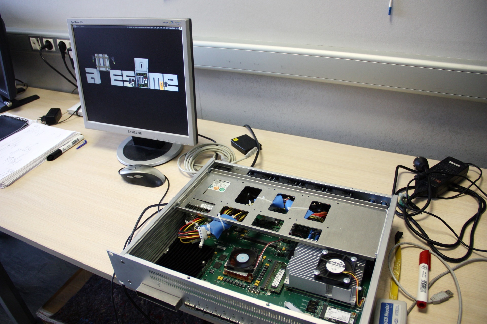
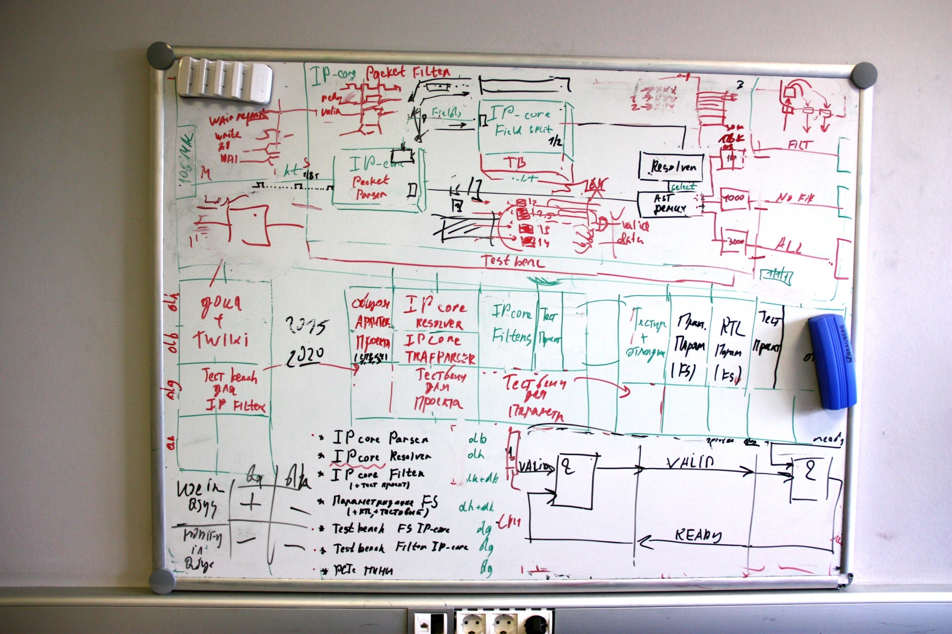
They say that if you look for a long time, it will not become clearer
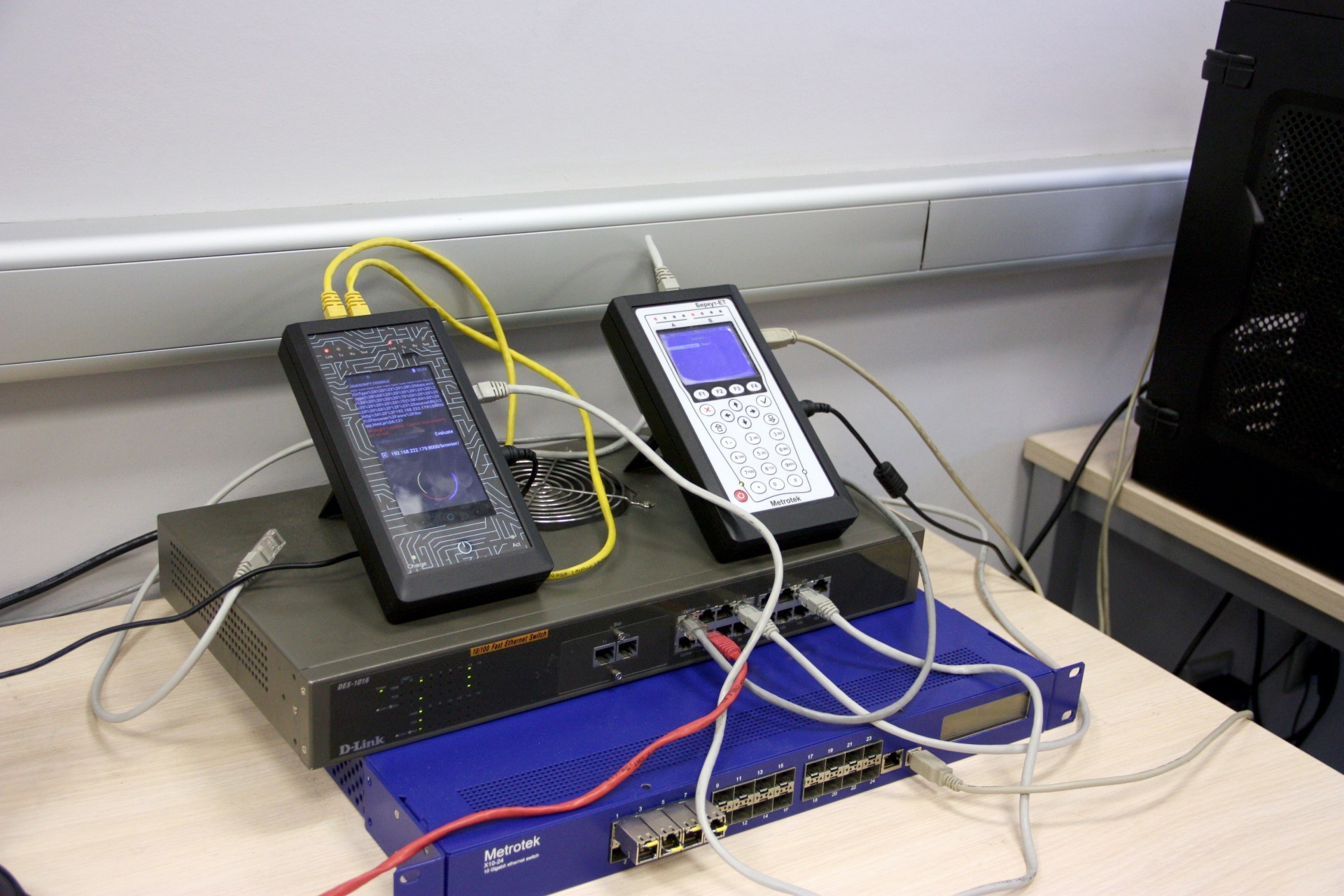
Exiting delightfully, we are heading towards the final stage - towards applied development.
This is the realm of Android, user menus and measurement interfaces. Everything written is tested here, on live equipment. The software is developed on the Apache Cordova platform, which interacts with the system through a previously written API using the USB / IP interface. The creators of the API are sitting at the next door, so that all issues are resolved very quickly.
Maybe I'm already tired, but once again I remind you that the set of tests implemented by the instruments and their algorithms are not taken from the ceiling, but strictly from the RFC and additions to them.
Test bench option
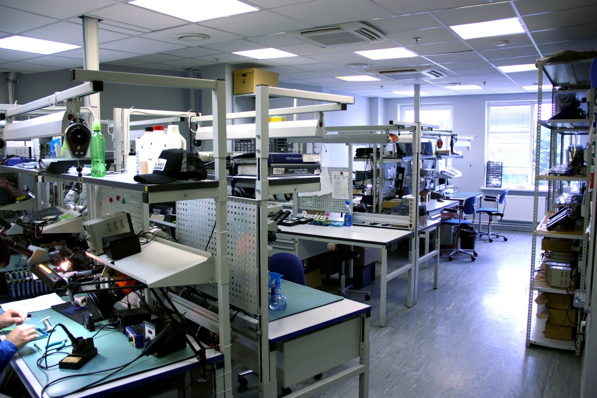
And finally the production
At the beginning of the article it was stated that the STC Metrotek does not occupy super large areas, but has its own production. The output power is at the level of provision of working samples of the designed devices and provision of small-scale assembly. But sometimes additional factors come into play — for example, the B100 board, just physically does not fit in the local soldering furnace, and buying a larger amount for the sake of single orders is meaningless.
Without a general view can not
Contrary to the established traditions, only men work on the installation here. This is probably a consequence of the very small-scale, when the tasks are not worth a day to sit on the conveyor and poke a soldering iron in the same place, the same parts.
Of course, it’s not by one manual assembly that the workshop is alive and they have a machine for mounting a small scatter. He stands in a separate clean room, quite happy with everything, although it does not hit performance. We found him in an uncharged state, sighed sadly and returned to the assembly hall.
Here it is, Chinese laborer
Conducting a further inspection of the premises, it was noted that in addition to the classic installation of parts on the board, the optical part of the OTDR was also being cooked to complete the OTDR testers with modules. Also, from the interesting, a workshop was created to create plastic cases, models of new devices or just to finish them in place. As popular wisdom says - after assembly, carefully process the file. Or even a circular.
When you see a circular, and behind the wall is mounting 0.1-0.2 elements
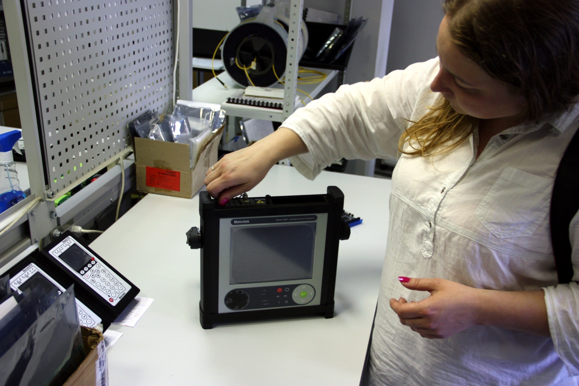
But we move further along the technological chain. After the device is assembled and the firmware is poured into it, everyone without exception is sent to a simple daily test - looped and included in the measurement test. If the day the fighter lasted and did not go smoke, it means fit for military service. According to statistics, a day is enough to identify all the problematic elements.
Testing testers at various stages of assembly
Each device has a passport, which starts simultaneously with the installation, which indicates its entire history, including who installed which items, who tested, calibrated, what firmware was installed, and so on. Keeping such strict reporting allows certification of devices for using their testimony as evidence in court. Now, your provider will answer for the braking tanchiki to the fullest extent!
It should be noted that all equipment is made as suitable as possible for the harsh conditions of field operation. For example, the MMT Eagle, which is a modular configurable platform, could be two times smaller, but for the sake of durability it was necessary to sacrifice miniature and pack it in a strong iron case. But the devices are certified according to the strength class and can be safely dropped to the floor several times a day.
Patient Golden Eagle MMT
After the tests, the instruments are packed and shipped to the customer. And here we are naturally surprised. The concept of good packaging has reached a new level. The most valuable equipment of STC Metrotek delivers exclusively in shock-resistant cases, without any exceptions. They can be safely thrown out of the window or planted on top of a young elephant. The electronics inside will remain intact, in its foam rubber kingdom.
Practice has shown that it is better to supply good equipment with a good suitcase. It is cheaper for itself, and customers who are accustomed to cardboard packaging feel a sense of genuine delight. Rumor has it that the most agile guys use these bags for travel. It is unlikely that your socks and T-shirts will feel more comfortable than in this suitcase.
B100 surrounded by care and gentleness
To the exit
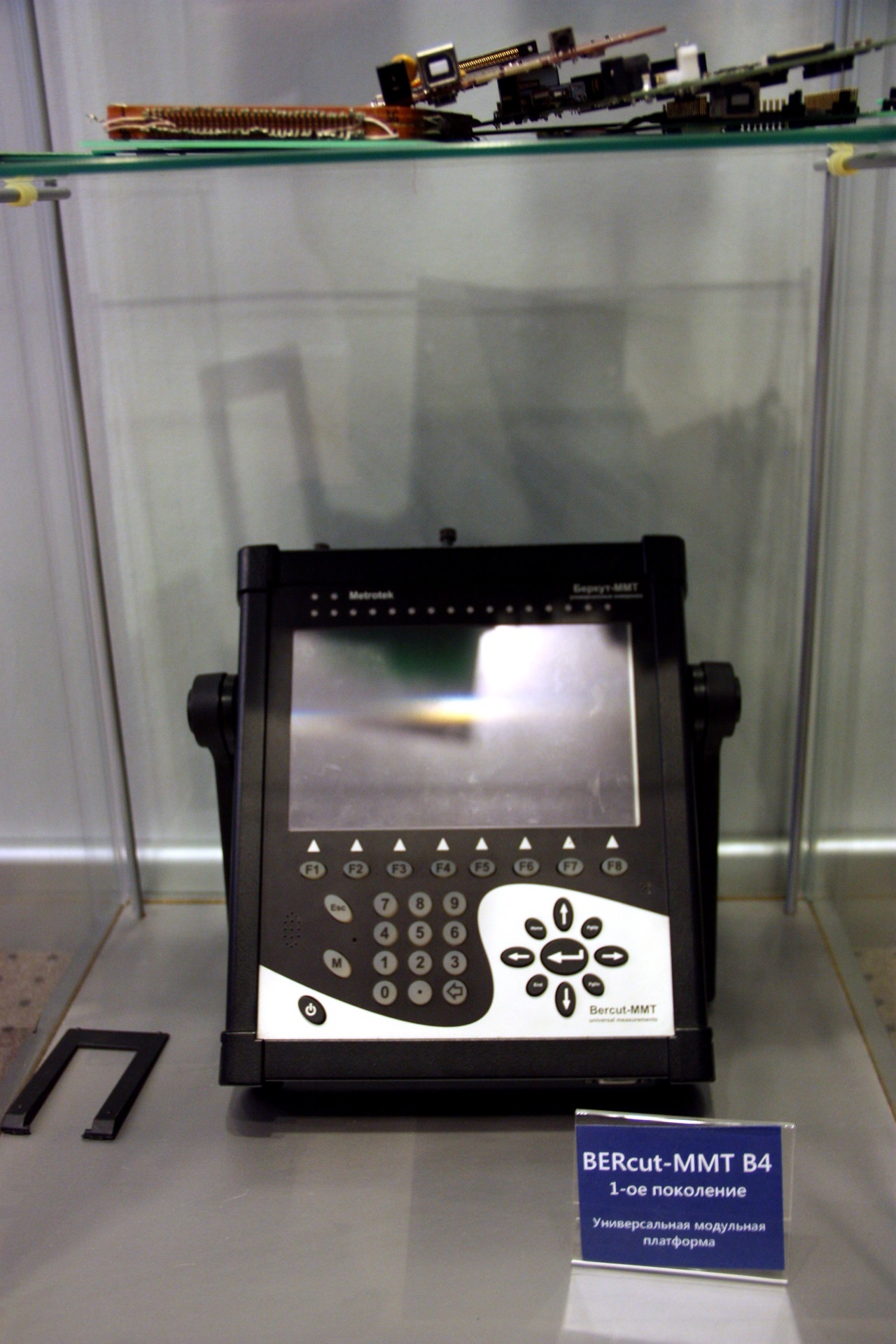
Finally, looked at the local museum, which collected samples of all previously produced devices. Of the interesting was noted BERcut-MMT, the first generation, the design of which from and to, was made solely by the developers.
Design from engineers. He exists.
A demo stand, which is in the process of reassembly, was not far behind, so it wasn’t enough to boast. Well, at least the top LEDs included.
Farewell and conclusions from what he saw
The entire Linkmeup edition loves telling success stories of telecommunication companies that have emerged in the post-Soviet space.
“STC Metrotek” can be safely called a pearl and set an example for everyone. This company conducts its business, not starting from the western giants of the industry, but actively competes with them and constantly produces advanced devices that meet the changing realities of modern times.
For example, their very first device, the Berkut-S, the compact E1 analyzer, based on the iPAQ, frankly surpassed its time. Then any analyzer had to get into a large backpack with difficulty, and at least two had to maintain it. Operators did not believe, took tests, were delighted and were afraid to give it to field engineers because or lose or steal. And then the iPAQ, as a platform, died at all, but the engineers of STC Metrotek did not give up, but continued to work hard, continuing to please all signalers with their devices.
Therefore, I sincerely want to wish the children further development, strengthen their presence in international markets and please us with a device that will first provide a new standard of testing not only in the CIS, but throughout the world as a minimum.
And while we go eat a cooling pizza and write this report.
Source: https://habr.com/ru/post/305632/
All Articles