Static time analysis demystified. Part 2
Many novice developers do not fully understand the meaning of such trigger parameters as Setup (Setup) and Hold (Hold). Quite a lot has been written about the metastability and nature of these two parameters ( https://habrahabr.ru/post/254869/ ), so we will focus on how to deal with Setup and Hold violations in the process of designing circuits.
In the beginning we give the definition of Setup and Hold:
Why am I writing about events on trigger inputs? Because static time analysis builds a graph to calculate delays, and the inputs of the elements are the vertices of this graph. More information about the construction of graphs and the internal “kitchen” of static time analysis can be found in the first article https://habrahabr.ru/post/273849/ .
Now, let's talk about how Setup and Hold violations are checked. In synchronous circuits, all transients begin at the clock input (or rather, at the output of an external oscillator or PLL, but the static analysis does not look beyond the limits of the microchip, so we are talking only about the clock input of the microchip). So, the transient (clock, clock pulse) propagates through the circuits to the clock inputs of the triggers, splitting into many transients that pass through the triggers to their outputs, enter the logic, and end at the inputs of these trigger receivers. The main condition for the operation of synchronous circuits: all transients must end in one cycle. Or, more precisely, not in one clock cycle, but by the time of arrival of the next clock pulse, which is actually different for each trigger, since the clock circuit in the real microchip is built on the principle of a tree.
About the tree. It is obvious that the clocking circuit has such a large number of loads that no logical element has enough power to pump all of them. Therefore, the clocking circuit is designed in the form of a tree, the top of which is the clock input of the microcircuit, the branches are power buffers or inverters, and the leaves are the clock inputs of the triggers. The tree is not perfect (it is often made that way specifically), therefore there is always the non-simultaneity of the arrival of tact on various triggers. Because of this, it turns out that in some parts of the circuit the transients must end earlier, and in other parts later - just to catch the time Tsetup before the arrival of the clock pulse. Let's look at the following picture (picture and formulas are borrowed from the English article http://www.edn.com/design/systems-design/4392195/Equations-and-Impacts-of-Setup-and-Hold-Time )
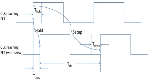
The picture shows the waveforms of the arrival of the clock pulse on the FF1 and FF2 triggers, between which there is a combination circuit that delays the signal. In other words, FF1 is a trigger signal source, FF2 is a receiver, and a signal through logic, depending on some input conditions, can reach both very quickly and very slowly. Let us deal with the following notation: Tskew is the skew of the clocking tree, due to which the clock to FF2 comes later than to FF1 by the value of Tskew. Tc2q - signal delay inside the trigger between the clock input and the data output. Let me remind you that in synchronous circuits, the source of all transients is a clock pulse, therefore the signal path goes through a clock input to the output of trigger data, and then through logic. Tcomb is the delay of the signal in logic, Tclk is the period of the clock pulse, and Tsetup is the trigger characteristic, the definition of which (Setup) was given above.
We look at the picture and see that the maximum end time of transients at the input of the trigger data should satisfy the following inequality (1):
Here Max (Tcomb) is the maximum possible Tcomb value. It follows from the formula that one can fight with the violation of inequality in two ways: move the time of arrival of a clock pulse to FF2 to the right, changing Tskew, or reduce the delay in Max logic (Tcomb).
Now let's try to deal with violations of Hold. If the Setup violation, generally speaking, is related to the next clock cycle, since it is compared with the moment of arrival of the next clock pulse, then the Hold violation should be checked already in the current clock cycle. How can a hold violation occur? According to the picture, if the signal from the FF1 output through the logic passes so quickly that it has time to spoil the data at the FF2 input, we will get a violation in the current clock cycle. Which implies the condition that the signal from the FF1 output cannot come faster than in the time of Thold, adjusted for Tskew. We obtain the inequality (2)
Here Min (Tcomb) is the minimum possible Tcomb value. It also follows from this formula that it is possible to fight with violation by moving Tskew or by increasing delays in the Min logic (Tcomb).
')
Next, let's talk about how CAD is struggling with the elimination of violations. Its primary task is to draw out the speed of the designed circuit. Suppose we need to get the frequency of the 1 GHz circuit, despite the fact that there is a delay of 1.2 ns in the design in a couple of places in the design. CAD can try to shrink this logic to 1 ns, or skew the clock tree in such a way that Tskew at the trigger receiver will be equal to 200 ps. Something similar is shown in the picture above. Since logic usually fails to squeeze, the first thing CAD does is rebuild a clock pulse tree, thereby eliminating violations of Tsetup. It should be noted that with an increase in Tskew, the risk of Hold is also increasing.
When the desired frequency is reached, the turn of the Hold fix begins. This time, the CAD does not touch the clock tree, and uses the second method - the increase in Min (Tcomb), i.e. minimum delays in logic where Hold violations are present. Delays increase very simply by inserting buffer elements. Although the excess buffers will certainly increase the consumption of the circuit.
It is curious that the increase in delays in the circuit due to heating, reducing power, accumulation of radiation dose, or aging, can be countered by reducing the operating frequency of the chip. Indeed, as can be seen from formula (1), if the delays increase, then Tclk should be reduced. But if the delays in the circuit are reduced, due to excessive cooling or an increase in the supply voltage, then violations of the Hold in the chip can not be fixed by anything - the chip simply stops working, which follows from formula (2). How, then, are chips designed for low and even ultralow temperatures? Most often, such schemes are designed in the usual way, but lay a huge stock of Hold. The larger the margin, the more the microcircuit can be cooled below the design temperatures, but to the extent that only the experiment will show. The probability of violations also decreases when the skewed clock tree is abandoned in favor of the most even (most commonly used so-called H-tree) with an attendant decrease in performance. And the most reliable way is to design asynchronous (SI, DI) circuits that are completely resistant to parametric faults.
Well, in conclusion, and what have the FPGA? First, there is no section on ASIC at habr. Secondly, a good FPGA will sooner or later grow to the ASIC design. And thirdly, though the FPGA has the ability to manipulate Clock Skew and is neutered, but they still exist. I hope someone article will be useful.
In the beginning we give the definition of Setup and Hold:
- Setup setup time is the minimum time from the moment of completion of transients at the data input to the moment when the clock edge arrives at the trigger input of the trigger.
- Hold Hold time is the minimum time from the arrival of the clock front at the clock input to the start of new transients at the trigger data input.
Why am I writing about events on trigger inputs? Because static time analysis builds a graph to calculate delays, and the inputs of the elements are the vertices of this graph. More information about the construction of graphs and the internal “kitchen” of static time analysis can be found in the first article https://habrahabr.ru/post/273849/ .
Now, let's talk about how Setup and Hold violations are checked. In synchronous circuits, all transients begin at the clock input (or rather, at the output of an external oscillator or PLL, but the static analysis does not look beyond the limits of the microchip, so we are talking only about the clock input of the microchip). So, the transient (clock, clock pulse) propagates through the circuits to the clock inputs of the triggers, splitting into many transients that pass through the triggers to their outputs, enter the logic, and end at the inputs of these trigger receivers. The main condition for the operation of synchronous circuits: all transients must end in one cycle. Or, more precisely, not in one clock cycle, but by the time of arrival of the next clock pulse, which is actually different for each trigger, since the clock circuit in the real microchip is built on the principle of a tree.
About the tree. It is obvious that the clocking circuit has such a large number of loads that no logical element has enough power to pump all of them. Therefore, the clocking circuit is designed in the form of a tree, the top of which is the clock input of the microcircuit, the branches are power buffers or inverters, and the leaves are the clock inputs of the triggers. The tree is not perfect (it is often made that way specifically), therefore there is always the non-simultaneity of the arrival of tact on various triggers. Because of this, it turns out that in some parts of the circuit the transients must end earlier, and in other parts later - just to catch the time Tsetup before the arrival of the clock pulse. Let's look at the following picture (picture and formulas are borrowed from the English article http://www.edn.com/design/systems-design/4392195/Equations-and-Impacts-of-Setup-and-Hold-Time )
The picture shows the waveforms of the arrival of the clock pulse on the FF1 and FF2 triggers, between which there is a combination circuit that delays the signal. In other words, FF1 is a trigger signal source, FF2 is a receiver, and a signal through logic, depending on some input conditions, can reach both very quickly and very slowly. Let us deal with the following notation: Tskew is the skew of the clocking tree, due to which the clock to FF2 comes later than to FF1 by the value of Tskew. Tc2q - signal delay inside the trigger between the clock input and the data output. Let me remind you that in synchronous circuits, the source of all transients is a clock pulse, therefore the signal path goes through a clock input to the output of trigger data, and then through logic. Tcomb is the delay of the signal in logic, Tclk is the period of the clock pulse, and Tsetup is the trigger characteristic, the definition of which (Setup) was given above.
We look at the picture and see that the maximum end time of transients at the input of the trigger data should satisfy the following inequality (1):
Tc2q + Max(Tcomb) + Tsetup ≤ Tclk + Tskew (1)
Here Max (Tcomb) is the maximum possible Tcomb value. It follows from the formula that one can fight with the violation of inequality in two ways: move the time of arrival of a clock pulse to FF2 to the right, changing Tskew, or reduce the delay in Max logic (Tcomb).
Now let's try to deal with violations of Hold. If the Setup violation, generally speaking, is related to the next clock cycle, since it is compared with the moment of arrival of the next clock pulse, then the Hold violation should be checked already in the current clock cycle. How can a hold violation occur? According to the picture, if the signal from the FF1 output through the logic passes so quickly that it has time to spoil the data at the FF2 input, we will get a violation in the current clock cycle. Which implies the condition that the signal from the FF1 output cannot come faster than in the time of Thold, adjusted for Tskew. We obtain the inequality (2)
Tc2q + Min(Tcomb) ≥ Thold + Tskew (2)
Here Min (Tcomb) is the minimum possible Tcomb value. It also follows from this formula that it is possible to fight with violation by moving Tskew or by increasing delays in the Min logic (Tcomb).
')
Next, let's talk about how CAD is struggling with the elimination of violations. Its primary task is to draw out the speed of the designed circuit. Suppose we need to get the frequency of the 1 GHz circuit, despite the fact that there is a delay of 1.2 ns in the design in a couple of places in the design. CAD can try to shrink this logic to 1 ns, or skew the clock tree in such a way that Tskew at the trigger receiver will be equal to 200 ps. Something similar is shown in the picture above. Since logic usually fails to squeeze, the first thing CAD does is rebuild a clock pulse tree, thereby eliminating violations of Tsetup. It should be noted that with an increase in Tskew, the risk of Hold is also increasing.
When the desired frequency is reached, the turn of the Hold fix begins. This time, the CAD does not touch the clock tree, and uses the second method - the increase in Min (Tcomb), i.e. minimum delays in logic where Hold violations are present. Delays increase very simply by inserting buffer elements. Although the excess buffers will certainly increase the consumption of the circuit.
It is curious that the increase in delays in the circuit due to heating, reducing power, accumulation of radiation dose, or aging, can be countered by reducing the operating frequency of the chip. Indeed, as can be seen from formula (1), if the delays increase, then Tclk should be reduced. But if the delays in the circuit are reduced, due to excessive cooling or an increase in the supply voltage, then violations of the Hold in the chip can not be fixed by anything - the chip simply stops working, which follows from formula (2). How, then, are chips designed for low and even ultralow temperatures? Most often, such schemes are designed in the usual way, but lay a huge stock of Hold. The larger the margin, the more the microcircuit can be cooled below the design temperatures, but to the extent that only the experiment will show. The probability of violations also decreases when the skewed clock tree is abandoned in favor of the most even (most commonly used so-called H-tree) with an attendant decrease in performance. And the most reliable way is to design asynchronous (SI, DI) circuits that are completely resistant to parametric faults.
Well, in conclusion, and what have the FPGA? First, there is no section on ASIC at habr. Secondly, a good FPGA will sooner or later grow to the ASIC design. And thirdly, though the FPGA has the ability to manipulate Clock Skew and is neutered, but they still exist. I hope someone article will be useful.
Source: https://habr.com/ru/post/302806/
All Articles