The interaction of software and hardware
Introduction
Understanding how a software variable takes the value of a physical signal and how the value of a program value turns into a specific signal can help software developers of control systems in calculating delays, solving optimization problems, ensuring sustainability, developing interfaces and connecting to processors and controllers of peripherals: sensors, actuators, etc.
This paper discusses issues related to the direct and inverse transformations “software variable - signal”: features of building data transmission channels, connecting peripherals to processor buses, address receiving data transmission issues and the operation of a hypothetical processor when exchanging data with an external device.
Formation of data transmission channel
Consider a data channel that has only two states, for example, the presence or absence of voltage. The transmitter should set the voltage in the line in accordance with the transmitted data, and the receiver on the measured voltage to highlight the data line. The simplest transmitter includes a voltage source and an ideal switch that, by changing its own resistance (zero or infinity), closes or disconnects the wires. A voltage meter (multimeter) with infinite input resistance is used as an ideal receiver.
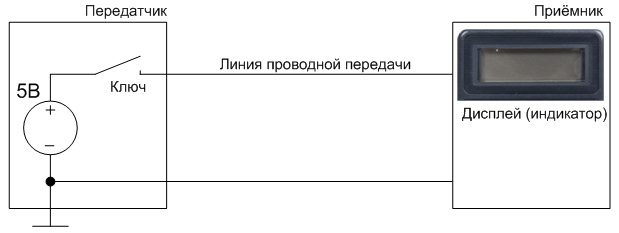
Fig. 1. Scheme with uncertain voltage in the transmission line. In a real circuit, the function of a key can be performed by a transistor.
')
In the scheme of Fig. 1 when the key is closed, a 5V source is transmitted to the receiver, however, when the key is open at the receiver input there is an unspecified voltage.
This uncertainty is not in the scheme. 2, which has two steady states 5B or 0V. Resistance R is added to the transmitter circuit to limit current through a closed key. The transition process in the line is proportional to the product of the capacity of the line on the output impedance of the transmitter, which is different when establishing and resetting the voltage in the line. When setting the voltage in the line, the capacity is charged through the resistance R. During the voltage drop, the capacity is discharged through the resistance of the closed key.
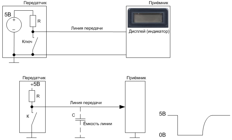
Fig. 2. Transfer of two states 5B and 0B. Identical schemes. The time constant (R * C) of the transition from 0V to 5V (capacity charge) is greater than the constant discharge of the line through an ideal switch with zero resistance.
To reduce the time for establishing the voltage, the resistor R is replaced by the key K1 (Fig. 3), the IS-NOT inverter is added to the circuit, which ensures the operation of the keys K1 and K2 in antiphase (one is closed, the other is open).
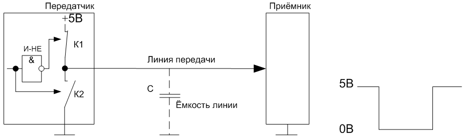
Fig. 3. Keys K1 and K2 minimize the time of transients. Inverter I-Not provides key operation in antiphase.
Data transfer problems
The serial data stream consists of zeros and ones. Let states 0B and 5B correspond to logical zero and one, respectively (Fig. 4). It is necessary that all transmitter data be received by the receiver without loss. For this
1. The transmitter and receiver must operate with the same period (at the same frequency).
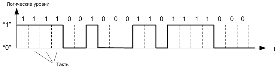
Fig. 4. Clocked sequential data transfer.
Suppose a line does not change its state for a long time and is under voltage of 5V. How to determine - “Does the transmitter transmit data 1111111111 ... or not?” To resolve this issue, the data transfer protocol should be supplemented with the following provisions.
2. In the absence of transmission, the line is energized (in the “1” state).
3. The transfer begins with a transition from 1 to zero.
4. The first clock after the transition does not contain data.
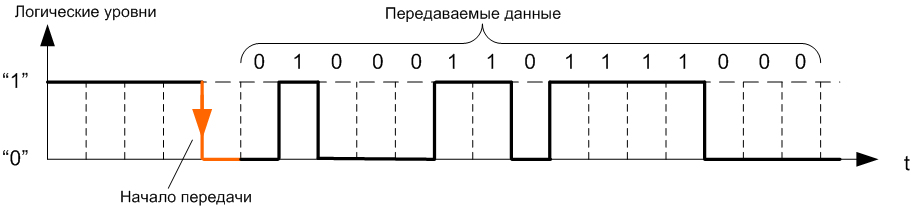
Fig. 5. Enter the start bit.
The longer the data sequence (packet length), the better the line performance. But, on the other hand, increasing the packet length tightens the requirements for synchronization of the transmitter and receiver and increases the sensitivity to interference in the line, which can change the transmitted sequence.
To detect false data, a checksum or other means to protect the data from loss is introduced into the sequence. In general, the packet length should be set according to the quality of the network equipment. An example of data transfer bytes is shown in Fig. 6. The performance of this line is 66% (as 100% * 8 data bits / 12 bit period).

Fig. 6. Byte-wise data transmission using RS-232 protocol.
For successful data transmission, the transmitter and receiver must have the same settings: clocking frequency, presence (absence) of the control bit, the same number of stop bits, etc.
Increasing the number of receivers and transmitters
Connecting to the line of additional receivers (Fig. 7) does not lead to data transmission failure if the total load on the transmitter does not exceed the limit.

Fig. 7. Connection to the transmission line of several receivers.
Combining transmitter outputs can cause an end-to-end current, as shown in Fig. 8. This current occurs when the transmitters simultaneously invert the inverse levels (low and high).
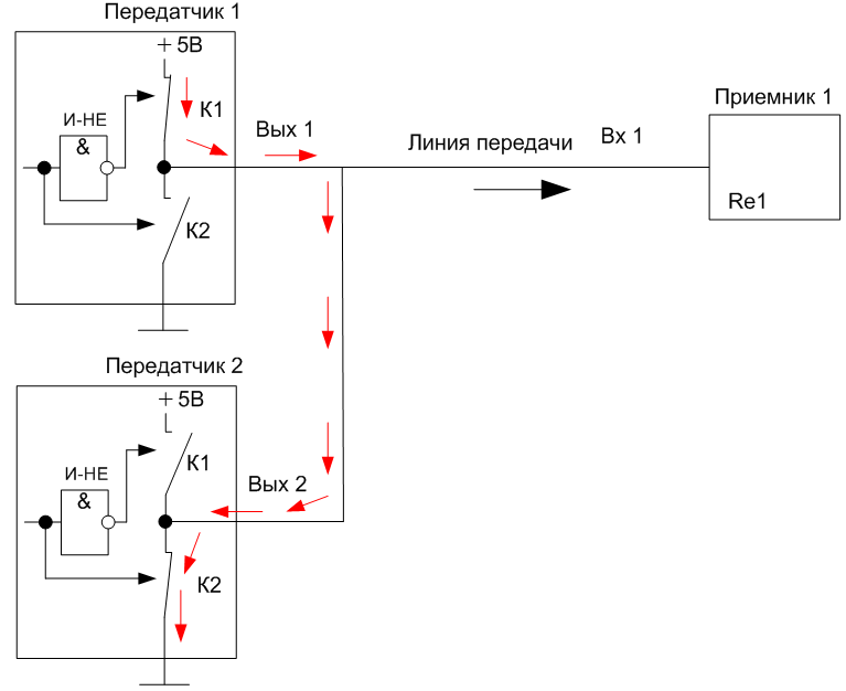
Fig. 8. Transmitters conflict with + 5V / 0V outputs. Red arrows indicate short circuit current.
Table. Transmission line states with two transmitters and a receiver.
Open collector transmitters (with a single lower key K2) can be connected to the transmission line in groups. When using transmitters with an open collector, the line should be “pulled” to the power source through a resistor, as shown in Fig. 9.

Fig. 9. Connecting several open collector transmitters to a common line.
Buffer and Register
Consider the principle of operation of the buffer and register used to connect receivers and transmitters to the processor data bus.
Buffer is an electronic device with parallel signal inputs and outputs. The outputs are connected to the corresponding inputs only for the duration of the control signal (Fig. 10). The rest of the time, the open collectors of the buffer keep it in a disconnected state from the output lines.
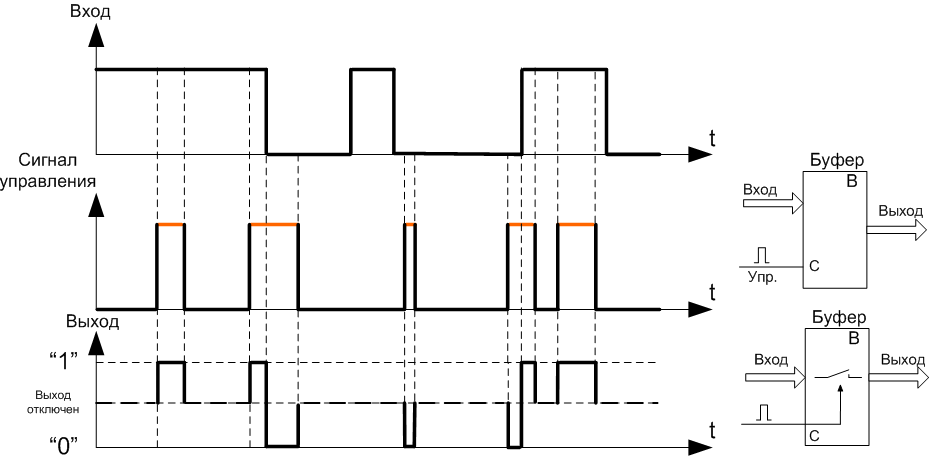
Fig. 10. Timing charts of the buffer.
Register is a device with memory (Fig. 11). At the time of the appearance of the control signal, the register sets the outputs of the input signals and holds the output signals unchanged until the next control signal appears, which again sets the values of the input signals at the outputs.
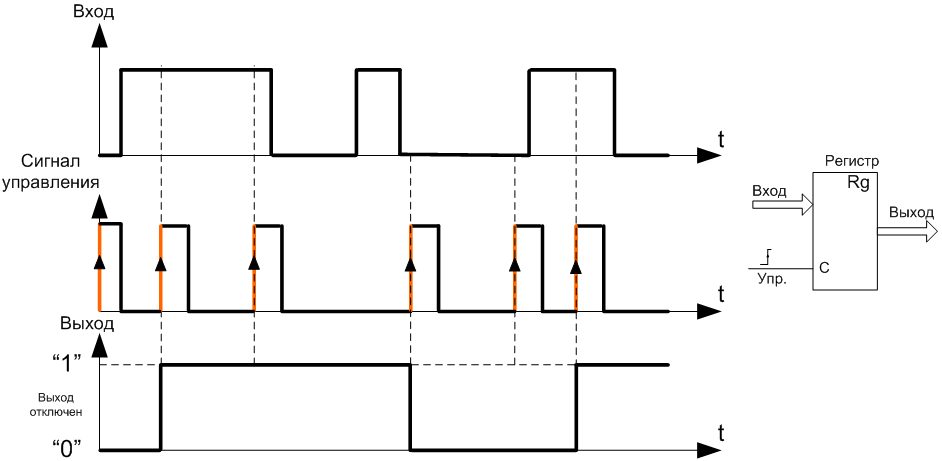
Fig. 11. The dependence of the output on the register input.
Address Decoder
Only two devices (receiver and transmitter) can participate in data exchange, even if several transmitters and / or receivers are connected to the line. To access the devices involved in the exchange of data, each device is assigned a unique address (device name). In parallel data transfer systems, the address data bus is used to access devices. The devices must include an address decoder, which monitors the status of the address bus and generates a signal at the output when the required address appears. The logic of the address decoder for the four-bit bus and one device with the address 1011 is shown in Fig. 12.

Fig. 12. Examples of address decoder logic for one device with address 1011.
Address decoder with multiple outputs (Fig. 13) activates only one output whose address is located at the input of the decoder.
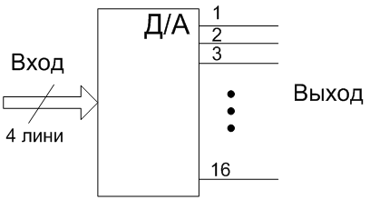
Fig. 13. Address decoder for 16 devices.
Write, read and connect port cycles
Reading and writing data are considered relative to the device controlling the data exchange process. If it is a processor, then “Write” means the transfer from the processor, and “Reading” means receiving by the processor.
To receive data from the device, the processor places the device address on the address bus, then the “Read” control signal RD and, after some time, reads the state of the data bus (Fig. 14). The external device, using the address decoder, must determine its addressing and, when requested by the RD processor, connect its own data through the buffer to the data bus and hold it on the bus no longer than the processor starts a new cycle.
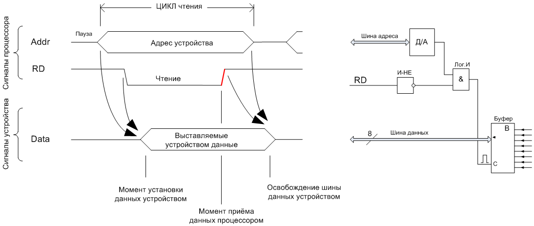
Fig. 14. Cycle of reading.
The write cycle also starts the processor by placing the device address on the address bus, then sets the data and reports this to the “Record” WR control signal (Fig. 15). The external device, having detected its own address on the address bus and having received from the processor a signal to write data WR, writes the state of the data bus to the register.
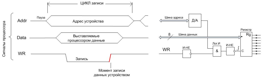
Fig. 15. Recording cycle.
External memory
If the output of the register of an external device is connected to the input of the buffer, then a memory cell will be obtained that can receive data, store and put data on the bus in a read cycle. The buffer and register can be connected to the common or separate outputs of the address decoder. In the first version (shown in Fig. 16), the data will be written and read at one address, in the second version, the data will be written at one address — and the written data will be read differently.

Fig. 16. External memory cell.
The structure of the hypothetical processor
The hypothetical processor (Fig. 17) includes the following main parts.
• Arithmetic Logical Device (ALU). Performs arithmetic and logical transformations.
• Battery. The register, saves the results of the ALU, communicates with devices connected to the data bus.
• command decoder. Analyzes instructions. Manages the command counter and starts the operation of the control circuit.
• Control scheme. Generates the necessary sequence of control signals that ensure the execution of operations.
• Processor registers. Store addresses and data.
• Control signals “Read” RD, “Write” WR, etc. They are used to control the transfer of data.
The processor requires program and data memory, which is connected to the processor via the address bus, data bus and control bus signals: “Read memory” and “Write to memory”. The program that the processor executes is in the program memory.
The processor has “Read I / O device” and “Write to I / O device” signals, which are used when accessing external devices - ports.
Address spaces of program memory and ports may overlap.
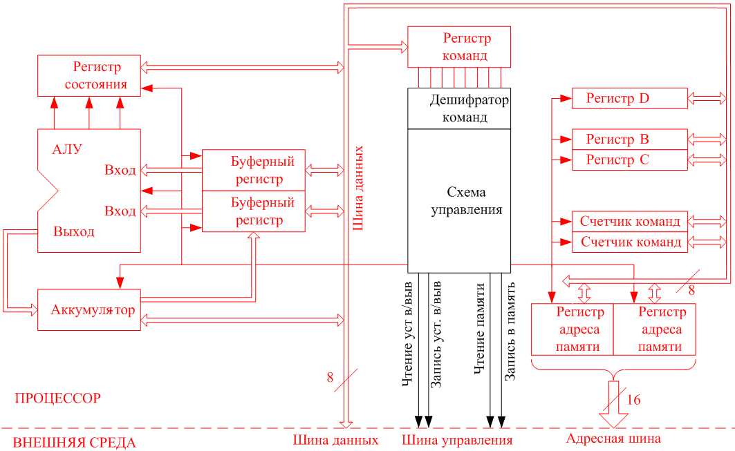
Fig. 17. The structure of the hypothetical processor [1].
The principle of organizing the management of program execution by a hypothetical processor contains the following provisions.
• The command code contains full information on what needs to be executed by the processor and where the next command is located.
• At the beginning of the operation, the processor command counter is assigned the value of the address of the first program command.
• The execution of a command includes the command sampling cycle and the execution cycle (s).
• In the sample cycle, the contents of the command counter are loaded into the memory address register, then the command from the external memory is transmitted via the data bus to the processor command register.
• In the execution loop, the command decoder determines the size of the command (the memory area occupied by the command in bytes), the control circuit sets the value of the address of the next command in the command counter by increasing the counter by the size of the command being executed.
• In a multibyte command, in addition to the command code, the addresses of the operands and / or the values of the operands are contained. When a multibyte instruction is executed, the memory address register is incremented by one, indicating the address of the command byte used, and the control circuit connects the corresponding memory cells to the processor registers.
• Transmission of commands and data via the data bus is carried out from the buffer-transmitter to the register-receiver, as discussed in Fig. 14, Fig. 15, Fig. sixteen.
I / O commands (access ports)
The list of processor commands includes port access commands, for example, for an x86 processor, these are the OUT and IN commands. When exchanging data with an external port, general registers DX and AX are involved. In DX, the port address is written, register AX is used for receiving and transmitting data.
An example of writing to the port at the address PORT_NUMBER of DATA data:
MOV DX, PORT_NUMBER; // Write the port address to the DX register
MOV AL, DATA; // Write data byte to low byte battery
OUT DX, AL; // Write to the port. The contents of the DX register are output to the address bus, and the contents of the AL register to the data bus. Sending data is synchronized with the “Write to I / O device” control signal.
An example of reading data from the port with the address PORT_NUMBER and storing it in the AL register.
MOV DX, PORT_NUMBER; // Write the port address to the DX register
IN AL, DX; // Read the port. The contents of the DX register are output to the address bus, then the “Read I / O device” control signal is set. The state of the data bus is written to the AL register at the time the control signal ends.
Note. 1. If there is no device or device data at the moment when the “Read I / O Device” signal ends, the processor writes the data bus status to AL. There are various schemes and algorithms to improve the reliability of reception / transmission, which are not considered here.
2. High-level languages have their own commands for communicating with ports or use assembly code inserts.
Example of step-by-step data exchange between the processor and external device ports
The interaction of software and hardware is shown in the example of executing a program by a hypothetical processor that communicates with an external device (Fig. 18).

Fig. 18. Processor with external memory and ports.
The program variable must be in the processor battery. The external device is assigned the address 378h, which is used for both reading and writing. The low-order signal on the external device buffer depends on the button state. An LED is connected to the low-order bit of the register output.
The LED should monitor the button state: turn on when the button is pressed and turn off when the button contacts are closed, and the program variable should monitor the status of the LED. To do this, the processor must read the external device signals from the buffer input into the battery, and then write the battery data to the external device register.
The program located at the zero address in the external memory connected to the processor contains the following commands.
• DOWNLOAD REGISTRATION PAIR DIRECT (LRP dx). Writes to the register DX processor data commands.
• READ PORT (IN al, dx). Transfers external device data to a low register battery. The address of the external device is taken from the register DX processor.
• RECORD TO PORT (OUT dx, al) transfers the low byte data of the battery to an external device. The address of the external device is in the register of the DX processor.
• TRANSITION (JMP). Go to the next command at the specified address.
At the beginning of the operation, the command counter is assigned the value of the starting address (entry point) of the program 0000.
Three-byte DOWNLOAD REGISTER PAIR DIRECT (LRP dx) command includes one command selection cycle and two execution cycles. In the sampling cycle, the contents of the command counter are loaded into the memory address register, whose value appears on the address bus and is decoded by the memory address decoder, which points to the zero memory location. When the “Read memory” signal is received, the external memory device places the contents of the zero cell on the data bus — the first command, which is written by the control circuit to the processor's command register. In the execution loop, when decoding a command, the control device increases the contents of the command counter by three — the size of the memory area occupied by the command in bytes. Now the counter points to the address of the following command, 0003. To access the second byte of the command, the processor control circuit increases the memory address register by one. Address 0001 is fed to the address bus. After receiving the address and control signal of the processor, the external memory device connects the contents of cell 0001 (03h number) to the data bus. The control circuit writes the number 03h to the high-order byte DH of the general-purpose register pair DX. The second half of the execution phase begins with increasing the memory address register by one to 0002, this memory location contains the third command byte (number 78h), which, like the previous two, goes to the data bus, the third byte value is written to the low byte DL of the DX processor pair. This ends the execution of the LRP dx command, as a result, the port address of the external device is in the DX register of the processor.
When the next IN al, dx command is executed in a sample cycle, the processor control circuit loads the contents of the command counter into the memory address register and sets the “Read memory” signal, the command from the third memory cell is written to the command register. In the command execution cycle, the control circuit increases the command counter by one byte — the size of the command, the counter indicates the address of the next command, 0004. Then the bytes of the DX register pair are sequentially written to the memory address registers, so the external device port address appears on the address bus. The decoders of both external memory and external device point to cell 378h, but, since the processor control circuit in accordance with the command code issues a “Read set. i / v ”and not“ Read memory ”, then only the external device buffer with the address 378h is connected to the data bus and the device signals, including the button state, go to the data bus through the buffer. The processor control circuit writes the contents of the data bus to a lower battery register.
After reading from the memory of the OUT dx, al command, the contents of the command counter are incremented by 1. Its contents are now 0005 — the address of the next JMP command. The contents of the register pair DX (0378h) is sent to the processor memory address register. The content of the low byte of the AL battery is placed on the data bus. When the “Rec. I / O ”this data from the bus is recorded in the register of the external device to which the LED is connected.
On the JUMP command (JMP), the new value 0003, the address of the first command of the next cycle, is loaded into the command counter from the second and third byte of the JMP command. Next, the IN al, dx, and other commands are executed. The described process is repeated until the processor stops.
Conclusion
The physical signal takes on the value of a program variable as a result of the “Write to the port” command being executed by the processor, which is accompanied by data transfer via the address bus, data transfer-data bus transfer and the formation of the corresponding control bus signal.
“Reading port” allows you to assign a value of a physical signal to a program variable. It also involves the transfer of data over the address bus and the data bus with the formation of a control signal — a read of an input / output device.
Similarly, variable conversion occurs in controllers or mini-computers in which external memory and / or ports are combined with a processor on a single chip or on a common board.
Literature
1. Introduction to microprocessor technology. Author: C. Gilmore Publisher: World Year: 1984 Pages: 314. Language: Russian.
2. Dr. Bob Davidov. Computer control technologies in the technical systems portalnp.ru/author/bobdavidov .
Understanding how a software variable takes the value of a physical signal and how the value of a program value turns into a specific signal can help software developers of control systems in calculating delays, solving optimization problems, ensuring sustainability, developing interfaces and connecting to processors and controllers of peripherals: sensors, actuators, etc.
This paper discusses issues related to the direct and inverse transformations “software variable - signal”: features of building data transmission channels, connecting peripherals to processor buses, address receiving data transmission issues and the operation of a hypothetical processor when exchanging data with an external device.
Formation of data transmission channel
Consider a data channel that has only two states, for example, the presence or absence of voltage. The transmitter should set the voltage in the line in accordance with the transmitted data, and the receiver on the measured voltage to highlight the data line. The simplest transmitter includes a voltage source and an ideal switch that, by changing its own resistance (zero or infinity), closes or disconnects the wires. A voltage meter (multimeter) with infinite input resistance is used as an ideal receiver.
Fig. 1. Scheme with uncertain voltage in the transmission line. In a real circuit, the function of a key can be performed by a transistor.
')
In the scheme of Fig. 1 when the key is closed, a 5V source is transmitted to the receiver, however, when the key is open at the receiver input there is an unspecified voltage.
This uncertainty is not in the scheme. 2, which has two steady states 5B or 0V. Resistance R is added to the transmitter circuit to limit current through a closed key. The transition process in the line is proportional to the product of the capacity of the line on the output impedance of the transmitter, which is different when establishing and resetting the voltage in the line. When setting the voltage in the line, the capacity is charged through the resistance R. During the voltage drop, the capacity is discharged through the resistance of the closed key.
Fig. 2. Transfer of two states 5B and 0B. Identical schemes. The time constant (R * C) of the transition from 0V to 5V (capacity charge) is greater than the constant discharge of the line through an ideal switch with zero resistance.
To reduce the time for establishing the voltage, the resistor R is replaced by the key K1 (Fig. 3), the IS-NOT inverter is added to the circuit, which ensures the operation of the keys K1 and K2 in antiphase (one is closed, the other is open).
Fig. 3. Keys K1 and K2 minimize the time of transients. Inverter I-Not provides key operation in antiphase.
Data transfer problems
The serial data stream consists of zeros and ones. Let states 0B and 5B correspond to logical zero and one, respectively (Fig. 4). It is necessary that all transmitter data be received by the receiver without loss. For this
1. The transmitter and receiver must operate with the same period (at the same frequency).
Fig. 4. Clocked sequential data transfer.
Suppose a line does not change its state for a long time and is under voltage of 5V. How to determine - “Does the transmitter transmit data 1111111111 ... or not?” To resolve this issue, the data transfer protocol should be supplemented with the following provisions.
2. In the absence of transmission, the line is energized (in the “1” state).
3. The transfer begins with a transition from 1 to zero.
4. The first clock after the transition does not contain data.
Fig. 5. Enter the start bit.
The longer the data sequence (packet length), the better the line performance. But, on the other hand, increasing the packet length tightens the requirements for synchronization of the transmitter and receiver and increases the sensitivity to interference in the line, which can change the transmitted sequence.
To detect false data, a checksum or other means to protect the data from loss is introduced into the sequence. In general, the packet length should be set according to the quality of the network equipment. An example of data transfer bytes is shown in Fig. 6. The performance of this line is 66% (as 100% * 8 data bits / 12 bit period).
Fig. 6. Byte-wise data transmission using RS-232 protocol.
For successful data transmission, the transmitter and receiver must have the same settings: clocking frequency, presence (absence) of the control bit, the same number of stop bits, etc.
Increasing the number of receivers and transmitters
Connecting to the line of additional receivers (Fig. 7) does not lead to data transmission failure if the total load on the transmitter does not exceed the limit.
Fig. 7. Connection to the transmission line of several receivers.
Combining transmitter outputs can cause an end-to-end current, as shown in Fig. 8. This current occurs when the transmitters simultaneously invert the inverse levels (low and high).
Fig. 8. Transmitters conflict with + 5V / 0V outputs. Red arrows indicate short circuit current.
Table. Transmission line states with two transmitters and a receiver.
| Out 1 | Out 2 | Bx 1 | Comment |
|---|---|---|---|
| 0 | 0 | 0 | |
| 0 | one | but. | Transmitter source 2 short circuit to transmitter 1 earth |
| one | 0 | but. | Transmitter source 1 short circuit to transmitter 2 ground |
| one | one | one |
Open collector transmitters (with a single lower key K2) can be connected to the transmission line in groups. When using transmitters with an open collector, the line should be “pulled” to the power source through a resistor, as shown in Fig. 9.
Fig. 9. Connecting several open collector transmitters to a common line.
Buffer and Register
Consider the principle of operation of the buffer and register used to connect receivers and transmitters to the processor data bus.
Buffer is an electronic device with parallel signal inputs and outputs. The outputs are connected to the corresponding inputs only for the duration of the control signal (Fig. 10). The rest of the time, the open collectors of the buffer keep it in a disconnected state from the output lines.
Fig. 10. Timing charts of the buffer.
Register is a device with memory (Fig. 11). At the time of the appearance of the control signal, the register sets the outputs of the input signals and holds the output signals unchanged until the next control signal appears, which again sets the values of the input signals at the outputs.
Fig. 11. The dependence of the output on the register input.
Address Decoder
Only two devices (receiver and transmitter) can participate in data exchange, even if several transmitters and / or receivers are connected to the line. To access the devices involved in the exchange of data, each device is assigned a unique address (device name). In parallel data transfer systems, the address data bus is used to access devices. The devices must include an address decoder, which monitors the status of the address bus and generates a signal at the output when the required address appears. The logic of the address decoder for the four-bit bus and one device with the address 1011 is shown in Fig. 12.
Fig. 12. Examples of address decoder logic for one device with address 1011.
Address decoder with multiple outputs (Fig. 13) activates only one output whose address is located at the input of the decoder.
Fig. 13. Address decoder for 16 devices.
Write, read and connect port cycles
Reading and writing data are considered relative to the device controlling the data exchange process. If it is a processor, then “Write” means the transfer from the processor, and “Reading” means receiving by the processor.
To receive data from the device, the processor places the device address on the address bus, then the “Read” control signal RD and, after some time, reads the state of the data bus (Fig. 14). The external device, using the address decoder, must determine its addressing and, when requested by the RD processor, connect its own data through the buffer to the data bus and hold it on the bus no longer than the processor starts a new cycle.
Fig. 14. Cycle of reading.
The write cycle also starts the processor by placing the device address on the address bus, then sets the data and reports this to the “Record” WR control signal (Fig. 15). The external device, having detected its own address on the address bus and having received from the processor a signal to write data WR, writes the state of the data bus to the register.
Fig. 15. Recording cycle.
External memory
If the output of the register of an external device is connected to the input of the buffer, then a memory cell will be obtained that can receive data, store and put data on the bus in a read cycle. The buffer and register can be connected to the common or separate outputs of the address decoder. In the first version (shown in Fig. 16), the data will be written and read at one address, in the second version, the data will be written at one address — and the written data will be read differently.
Fig. 16. External memory cell.
The structure of the hypothetical processor
The hypothetical processor (Fig. 17) includes the following main parts.
• Arithmetic Logical Device (ALU). Performs arithmetic and logical transformations.
• Battery. The register, saves the results of the ALU, communicates with devices connected to the data bus.
• command decoder. Analyzes instructions. Manages the command counter and starts the operation of the control circuit.
• Control scheme. Generates the necessary sequence of control signals that ensure the execution of operations.
• Processor registers. Store addresses and data.
• Control signals “Read” RD, “Write” WR, etc. They are used to control the transfer of data.
The processor requires program and data memory, which is connected to the processor via the address bus, data bus and control bus signals: “Read memory” and “Write to memory”. The program that the processor executes is in the program memory.
The processor has “Read I / O device” and “Write to I / O device” signals, which are used when accessing external devices - ports.
Address spaces of program memory and ports may overlap.
Fig. 17. The structure of the hypothetical processor [1].
The principle of organizing the management of program execution by a hypothetical processor contains the following provisions.
• The command code contains full information on what needs to be executed by the processor and where the next command is located.
• At the beginning of the operation, the processor command counter is assigned the value of the address of the first program command.
• The execution of a command includes the command sampling cycle and the execution cycle (s).
• In the sample cycle, the contents of the command counter are loaded into the memory address register, then the command from the external memory is transmitted via the data bus to the processor command register.
• In the execution loop, the command decoder determines the size of the command (the memory area occupied by the command in bytes), the control circuit sets the value of the address of the next command in the command counter by increasing the counter by the size of the command being executed.
• In a multibyte command, in addition to the command code, the addresses of the operands and / or the values of the operands are contained. When a multibyte instruction is executed, the memory address register is incremented by one, indicating the address of the command byte used, and the control circuit connects the corresponding memory cells to the processor registers.
• Transmission of commands and data via the data bus is carried out from the buffer-transmitter to the register-receiver, as discussed in Fig. 14, Fig. 15, Fig. sixteen.
I / O commands (access ports)
The list of processor commands includes port access commands, for example, for an x86 processor, these are the OUT and IN commands. When exchanging data with an external port, general registers DX and AX are involved. In DX, the port address is written, register AX is used for receiving and transmitting data.
An example of writing to the port at the address PORT_NUMBER of DATA data:
MOV DX, PORT_NUMBER; // Write the port address to the DX register
MOV AL, DATA; // Write data byte to low byte battery
OUT DX, AL; // Write to the port. The contents of the DX register are output to the address bus, and the contents of the AL register to the data bus. Sending data is synchronized with the “Write to I / O device” control signal.
An example of reading data from the port with the address PORT_NUMBER and storing it in the AL register.
MOV DX, PORT_NUMBER; // Write the port address to the DX register
IN AL, DX; // Read the port. The contents of the DX register are output to the address bus, then the “Read I / O device” control signal is set. The state of the data bus is written to the AL register at the time the control signal ends.
Note. 1. If there is no device or device data at the moment when the “Read I / O Device” signal ends, the processor writes the data bus status to AL. There are various schemes and algorithms to improve the reliability of reception / transmission, which are not considered here.
2. High-level languages have their own commands for communicating with ports or use assembly code inserts.
Example of step-by-step data exchange between the processor and external device ports
The interaction of software and hardware is shown in the example of executing a program by a hypothetical processor that communicates with an external device (Fig. 18).
Fig. 18. Processor with external memory and ports.
The program variable must be in the processor battery. The external device is assigned the address 378h, which is used for both reading and writing. The low-order signal on the external device buffer depends on the button state. An LED is connected to the low-order bit of the register output.
The LED should monitor the button state: turn on when the button is pressed and turn off when the button contacts are closed, and the program variable should monitor the status of the LED. To do this, the processor must read the external device signals from the buffer input into the battery, and then write the battery data to the external device register.
The program located at the zero address in the external memory connected to the processor contains the following commands.
• DOWNLOAD REGISTRATION PAIR DIRECT (LRP dx). Writes to the register DX processor data commands.
• READ PORT (IN al, dx). Transfers external device data to a low register battery. The address of the external device is taken from the register DX processor.
• RECORD TO PORT (OUT dx, al) transfers the low byte data of the battery to an external device. The address of the external device is in the register of the DX processor.
• TRANSITION (JMP). Go to the next command at the specified address.
At the beginning of the operation, the command counter is assigned the value of the starting address (entry point) of the program 0000.
Three-byte DOWNLOAD REGISTER PAIR DIRECT (LRP dx) command includes one command selection cycle and two execution cycles. In the sampling cycle, the contents of the command counter are loaded into the memory address register, whose value appears on the address bus and is decoded by the memory address decoder, which points to the zero memory location. When the “Read memory” signal is received, the external memory device places the contents of the zero cell on the data bus — the first command, which is written by the control circuit to the processor's command register. In the execution loop, when decoding a command, the control device increases the contents of the command counter by three — the size of the memory area occupied by the command in bytes. Now the counter points to the address of the following command, 0003. To access the second byte of the command, the processor control circuit increases the memory address register by one. Address 0001 is fed to the address bus. After receiving the address and control signal of the processor, the external memory device connects the contents of cell 0001 (03h number) to the data bus. The control circuit writes the number 03h to the high-order byte DH of the general-purpose register pair DX. The second half of the execution phase begins with increasing the memory address register by one to 0002, this memory location contains the third command byte (number 78h), which, like the previous two, goes to the data bus, the third byte value is written to the low byte DL of the DX processor pair. This ends the execution of the LRP dx command, as a result, the port address of the external device is in the DX register of the processor.
When the next IN al, dx command is executed in a sample cycle, the processor control circuit loads the contents of the command counter into the memory address register and sets the “Read memory” signal, the command from the third memory cell is written to the command register. In the command execution cycle, the control circuit increases the command counter by one byte — the size of the command, the counter indicates the address of the next command, 0004. Then the bytes of the DX register pair are sequentially written to the memory address registers, so the external device port address appears on the address bus. The decoders of both external memory and external device point to cell 378h, but, since the processor control circuit in accordance with the command code issues a “Read set. i / v ”and not“ Read memory ”, then only the external device buffer with the address 378h is connected to the data bus and the device signals, including the button state, go to the data bus through the buffer. The processor control circuit writes the contents of the data bus to a lower battery register.
After reading from the memory of the OUT dx, al command, the contents of the command counter are incremented by 1. Its contents are now 0005 — the address of the next JMP command. The contents of the register pair DX (0378h) is sent to the processor memory address register. The content of the low byte of the AL battery is placed on the data bus. When the “Rec. I / O ”this data from the bus is recorded in the register of the external device to which the LED is connected.
On the JUMP command (JMP), the new value 0003, the address of the first command of the next cycle, is loaded into the command counter from the second and third byte of the JMP command. Next, the IN al, dx, and other commands are executed. The described process is repeated until the processor stops.
Conclusion
The physical signal takes on the value of a program variable as a result of the “Write to the port” command being executed by the processor, which is accompanied by data transfer via the address bus, data transfer-data bus transfer and the formation of the corresponding control bus signal.
“Reading port” allows you to assign a value of a physical signal to a program variable. It also involves the transfer of data over the address bus and the data bus with the formation of a control signal — a read of an input / output device.
Similarly, variable conversion occurs in controllers or mini-computers in which external memory and / or ports are combined with a processor on a single chip or on a common board.
Literature
1. Introduction to microprocessor technology. Author: C. Gilmore Publisher: World Year: 1984 Pages: 314. Language: Russian.
2. Dr. Bob Davidov. Computer control technologies in the technical systems portalnp.ru/author/bobdavidov .
Source: https://habr.com/ru/post/281887/
All Articles