Creating a simple game based on FPGA
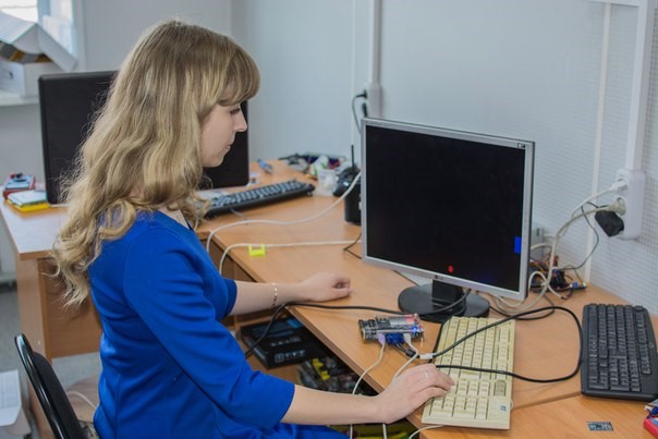
Hi Habr. I began studying FPGA quite recently. One of my projects, which focused on the PS / 2 and VGA interfaces, was a Pin-Pong game for one person. One of the implementations of which works on the DE0-CV board, which was kindly provided by the wonderful Silicon Russia project as part of the competition ( http://www.silicon-russia.com/2015/12/11/board-giveaway-for-mipsfpga/ ) .
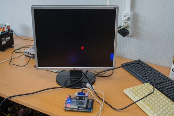
The essence of the game: there is a slider controlled from the keyboard, which should beat the ball moving around the screen. The VGA display was selected as the display medium, and the keyboard was selected with a simple PS / 2 interface. The score of the game itself is displayed on a seven-segment display.
Debug board
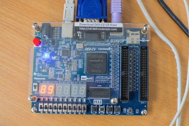
DE0-CV is the official debugging board distributed by Alter, its price is $ 150, and for academic fees it is $ 99. On the board itself we have:
')
- six seven-segment indicators, 10 LEDs, 10 switches, 4 buttons;
- VGA connector, PS / 2 connector, slot for micro SD card;
- SDRAM memory with a capacity of 64 MB;
- two GPIO connectors for 35 pins each.
Work logic
The program can be divided into 4 main blocks. Each of which performs a specific function.
- PLL is a ready-made ip block for receiving synchronizing pulses bypassed for clocking the system.
- PS / 2 is a block, the input of which receives signals from the PS / 2 port and is converted into codes of pressed keys.
- vga - block - driver for working with VGA monitor
- game - directly the implementation of the logic of the game. The inputs come signals from vga, ps2 and pll blocks.
The heart of the whole program is PLL. Thanks to its proper setup, you can work with VGA and clocking other blocks.

PS / 2 keyboard controller
To control the racket in the game, we use a keyboard with a PS / 2 interface. Before proceeding to review the implementation of the block, let's go over the PS / 2 protocol a bit.
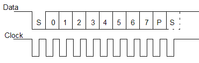
The pins used to communicate in the PS / 2 protocol are Data and Clock. The sending of bits consists of: one start bit, 8 data bits, a parity bit and a stop bit. The Clock output is clocking, as you might guess.
The setting of bits on the device side occurs on the leading edge, the rising edge of the Clock, and the reading on the device side on the falling edge of the signal. When the device does not transmit anything, Clock and Data are pulled to power. Then the Data bus and Clock go to zero, which is a sign that the message has been sent. After reading 8 bits, there is a parity bit and a stop bit, which is always equal to one.
In the first handler, we count clock cycles in order to understand whether the button is pressed or not. If PS2_CLK_in is set for 52,500,000 cycles, the button is not pressed. Also here we check the codes of the keys pressed:
- if the key code of the pressed key coincides with the key code of the up arrow, the output up goes to 1;
- if the down arrow key is pressed, the output down goes to 1.
always @(negedge clock) begin if(PS2_CLK_in == 1) count_clk <= count_clk + 1; else count_clk <= 0; if(count_clk>=52500000) begin led_out <= 0; end else led_out <= bit; if(led_out == 8'b01110010) begin down <= 1; up <= 0; end else if(led_out == 8'b01110101) begin up <= 1; down <= 0; end else begin down <= 0; up <= 0; end end If the transition from the high level to the low level is detected at the input PS2_CLK_in, then the state is read from the input PS2_DAT_in.
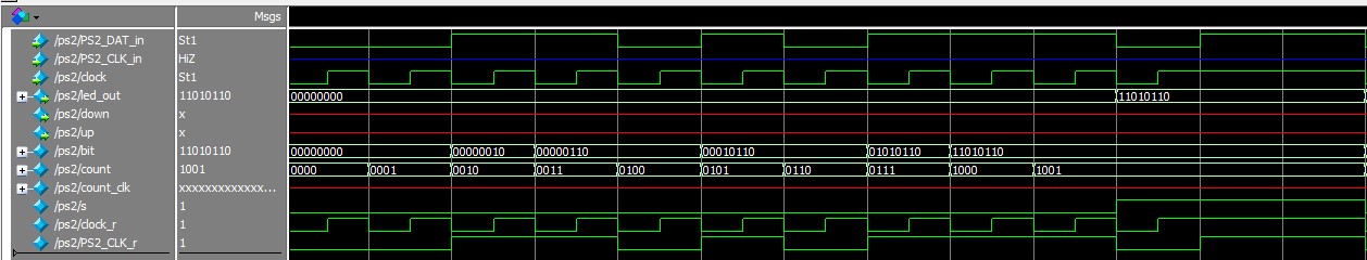
always @(negedge PS2_CLK_in) begin if(s == 0) begin if(count<=7) begin bit <= bit|(PS2_DAT_in<<count); end if(count == 9) begin s <= 1; end else begin count <= count + 1; end end if(s == 1) if(PS2_DAT_in == 0) begin s <= 0; count <= 0; bit <= 0; end end endmodule The code for testing in the ModelSim environment is shown below:
initial begin #0 clock_r=1; #275 clock_r = 1; //s repeat( 22 ) begin #25 clock_r=~clock_r; end #100 clock_r = 1; repeat( 22 ) begin #25 clock_r=~clock_r; end #300 clock_r = 1; repeat( 22 ) begin #25 clock_r=~clock_r; end #50 clock_r = 1; repeat( 22 ) begin #25 clock_r=~clock_r; end end initial begin #250 PS2_CLK_r = 1; //s #50 PS2_CLK_r = 0; //start #50 PS2_CLK_r = 0; //0 #50 PS2_CLK_r = 1; //1 #50 PS2_CLK_r = 1; //2 #50 PS2_CLK_r = 0; //3 #50 PS2_CLK_r = 1; //4 #50 PS2_CLK_r = 0; //5 #50 PS2_CLK_r = 1; //6 #50 PS2_CLK_r = 1; //7 #50 PS2_CLK_r = 1; //parity bit #50 PS2_CLK_r = 0; //stop #50 PS2_CLK_r = 1; //s #50 PS2_CLK_r = 1; //s #50 PS2_CLK_r = 0; //start #50 PS2_CLK_r = 1; //0 #50 PS2_CLK_r = 1; //1 #50 PS2_CLK_r = 0; //2 #50 PS2_CLK_r = 0; //3 #50 PS2_CLK_r = 1; //4 #50 PS2_CLK_r = 0; //5 #50 PS2_CLK_r = 1; //6 #50 PS2_CLK_r = 1; //7 #50 PS2_CLK_r = 1; //parity bit #50 PS2_CLK_r = 0; //stop #50 PS2_CLK_r = 1; //s #250 PS2_CLK_r = 1; //s #50 PS2_CLK_r = 0; //start #50 PS2_CLK_r = 0; //0 #50 PS2_CLK_r = 1; //1 #50 PS2_CLK_r = 1; //2 #50 PS2_CLK_r = 1; //3 #50 PS2_CLK_r = 1; //4 #50 PS2_CLK_r = 1; //5 #50 PS2_CLK_r = 1; //6 #50 PS2_CLK_r = 1; //7 #50 PS2_CLK_r = 1; //parity bit #50 PS2_CLK_r = 0; //stop #50 PS2_CLK_r = 1; //s #50 PS2_CLK_r = 0; //start #50 PS2_CLK_r = 0; //0 #50 PS2_CLK_r = 1; //1 #50 PS2_CLK_r = 1; //2 #50 PS2_CLK_r = 0; //3 #50 PS2_CLK_r = 1; //4 #50 PS2_CLK_r = 0; //5 #50 PS2_CLK_r = 1; //6 #50 PS2_CLK_r = 1; //7 #50 PS2_CLK_r = 1; //parity bit #50 PS2_CLK_r = 0; //stop #50 PS2_CLK_r = 1; //s #50 PS2_CLK_r = 1; //s #50 PS2_CLK_r = 1; //s end assign clock = clock_r; assign PS2_DAT_in = PS2_CLK_r; Block behavior patterns:
Work VGA-block.
The DE0 board is equipped with a VGA output, as a DAC, for RGB outputs, using a simple circuit on resistors.
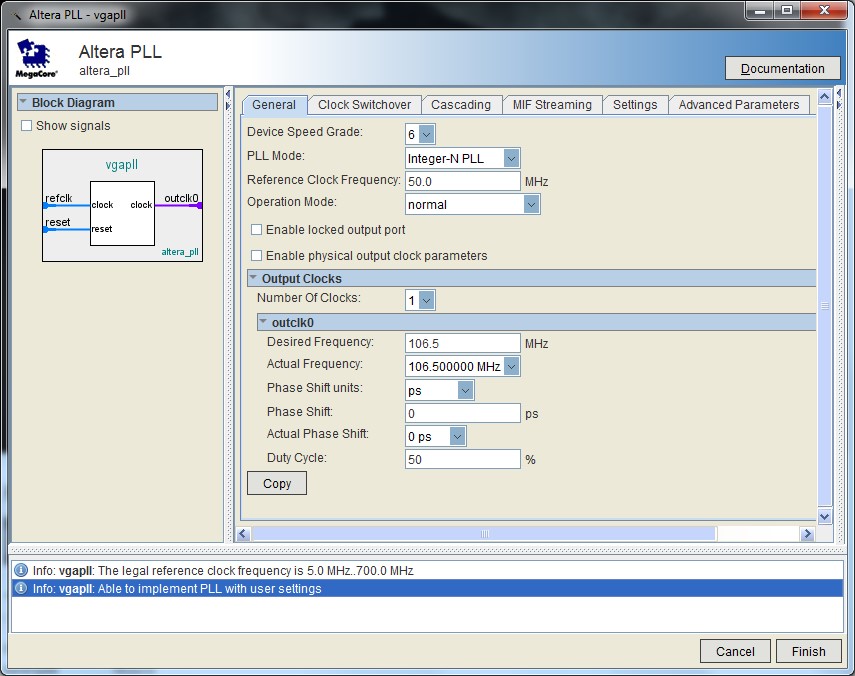
To get started with VGA, we need to look into the VESA specification (http://tinyvga.com/vga-timing) and select the desired mode of operation. View the required frequency and timings. Select the video mode 1440x900 60Hz. The required clock frequency is 106.5 MHz.
The board is set to 50 MHz quartz. With the help of a special PLL block, we can convert 50 MHz to 106.5. To do this, we need to pull the necessary block onto the working area and configure it.
From the documentation we take the necessary timings:
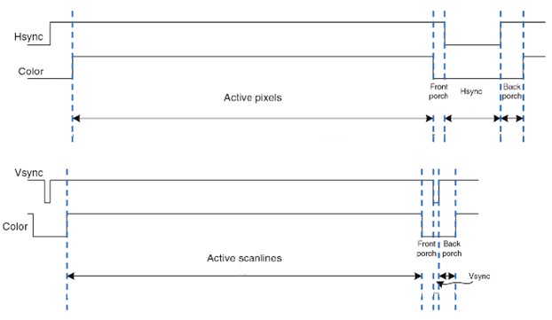
parameter h_front_porch = 80; parameter h_sync = 152; parameter h_back_porch = 232; parameter h_active_pixels = 1440; parameter v_front_porch = 3; parameter v_sync = 6; parameter v_back_porch = 25; parameter v_active_scanilines = 900; At each positive front of the pixel_clock input, we increase the pixel_count counter by one and, depending on its value, set the required logic level to the horizontal synchronization output hsync.
wire w_hsync = (pixel_count < h_sync); always @(posedge pixel_clock) begin hsync <= (pixel_count < h_sync); hvisible <= (pixel_count >= (h_sync+h_back_porch)) && (pixel_count < (h_sync+h_back_porch+h_active_pixels)); if(pixel_count < (h_sync+h_back_porch+h_active_pixels+h_front_porch) ) begin pixel_count <= pixel_count + 1'b1; char_count <= pixel_count; end else begin pixel_count <= 0; end end When the pixel_count counter reaches the end of the line, the line_count line counter increases and, depending on the parameters specified earlier, the required values are set to the output of the vertical sync vsync.
wire w_hsync_buf = w_hsync&~hsync; always @(posedge pixel_clock) begin if(w_hsync_buf)begin vsync <= (line_count < v_sync); vvisible <= (line_count >= (v_sync+v_back_porch)) && (line_count < (v_sync+v_back_porch+v_active_scanilines)); if(line_count < (v_sync+v_back_porch+v_active_scanilines+v_front_porch) )begin line_count <= line_count + 1'b1; line_count_out <= line_count; end else begin line_state <= 0; line_count <= 0; end end end When pixel_count and line_count fall into the range belonging to the visible part of the screen, then visible is set to a high level, thereby allowing the game block to start drawing the playing field:
always @* begin visible <= hvisible & vvisible; end Job game block.
The transition of the pixel_state signal to a logical unit means receiving permission to draw the playing field from the vga-block. The input signals char_count and line_count inform us about the coordinates of the point that is being drawn on the screen at the moment. Based on the coordinates of the ball and the racket, paint over the desired colors of the area that corresponds to them.
always @(pixel_state) begin if((char_count>=start_horz) && (char_count<=start_horz+50))begin if((line_count>=i) && (line_count<=i+100)) begin VGA_BLUE<=6'b111110; end else VGA_BLUE<=6'b000000; end else VGA_BLUE<=6'b000000; if((ball_x-char_count)*(ball_x-char_count)+(ball_y-line_count)*(ball_y-line_count)<400) VGA_RED<=5'b11110; else VGA_RED<=5'b00000; end Recalculation of the coordinates of the ball and racket occurs when the rising edge of the clock signal clk. Also, if the ball collides with the wall, there is a change in its direction of movement.
always @(posedge clk) begin if(key_2==0) begin if(i<vert_sync+vert_back_porch+vert_addr_time) i=i+1; else i=0; end if(key_0==0) begin if(i>vert_sync+vert_back_porch) i=i-1; else i=vert_sync+vert_back_porch+vert_addr_time; end if(flag == 2'b00) begin ball_x=ball_x-1; ball_y=ball_y-1; end if(flag == 2'b01) begin ball_x=ball_x+1; ball_y=ball_y+1; end if(flag == 2'b10) begin ball_x=ball_x-1; ball_y=ball_y+1; end if(flag == 2'b11) begin ball_x=ball_x+1; ball_y=ball_y-1; end if(ball_y<=vert_sync+vert_back_porch) if(flag==2'b00) flag=2'b10; else flag=2'b01; if(ball_x<=horz_sync+horz_back_porch) if(flag==2'b10) flag = 2'b01; else flag = 2'b11; if(ball_y>=vert_sync+vert_back_porch+vert_addr_time) if(flag==2'b01) flag=2'b11; else flag=2'b00; if(ball_x>=start_horz && ball_y>=i && ball_y<=i+100) if(flag==2'b11) flag=2'b00; else flag=2'b10; if(ball_x>=horz_sync+horz_back_porch+horz_addr_time) begin if(goal_2==9) begin goal_2<=0; goal<=goal+1; end else goal_2<=goal_2+1; if(flag==2'b11) flag<=2'b00; else flag<=2'b10; end end When:
- if the ball did not meet with the racket when approaching the right edge of the playing field, the score displayed on the seven-segment indicators will increase by one, because the response to a change in goal occurs;
- overflow goal - occurs: change of goal_2 and increase by one decimal place.
always @(clk) begin case(goal) 0: HEX_1 <= 7'b1000000; 1: HEX_1 <= 7'b1111001; 2: HEX_1 <= 7'b0100100; 3: HEX_1 <= 7'b0110000; 4: HEX_1 <= 7'b0011001; 5: HEX_1 <= 7'b0010010; 6: HEX_1 <= 7'b0000010; 7: HEX_1<= 7'b1111000; 8: HEX_1 <= 7'b0000000; 9: HEX_1 <= 7'b0010000; default: HEX_1 <= 7'b1111111; endcase end always @(clk) begin case(goal_2) 0: HEX_2 <= 7'b1000000; 1: HEX_2 <= 7'b1111001; 2: HEX_2 <= 7'b0100100; 3: HEX_2 <= 7'b0110000; 4: HEX_2 <= 7'b0011001; 5: HEX_2 <= 7'b0010010; 6: HEX_2 <= 7'b0000010; 7: HEX_2 <= 7'b1111000; 8: HEX_2 <= 7'b0000000; 9: HEX_2<= 7'b0010000; default: HEX_2 <= 7'b1111111; endcase end Conclusion
We synthesize the resulting project and obtain statistics on the resources employed in the FPGA:
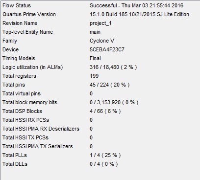
Implementing this project, we saw that using FPGA it is quite simple to implement complex interfaces such as VGA, with very high timing requirements that are difficult to withstand using the MK. https://github.com/MIPSfpga/pre-mipsfpga/tree/master/pinpong
PS: I entered the world of FPGA recently, very much apologize to the more experienced people that my code burned out my eyes. Please understand, forgive, help with advice.
Source: https://habr.com/ru/post/281549/
All Articles